SlideShare une entreprise Scribd logo
1  sur  6
Télécharger pour lire hors ligne
ECE 593 Project 1 By: Chien Chun Yao and Karthikvel Rathinavel
Introduction:
This report describes a method to design and layout a Wilkinson combiner by first using a microstip transmission line and
then using a coplanar waveguide. A two way Wilkinson power divider works by dividing the power coming from one port
and splitting it equally into two parts if it splits into a quarter wavelength in both sides and a shunted resistor between the
ports. It can be shown that if the input characteristic impedance is 50 ohms, then for a shunted resistor of 100 ohms the
output transmission lines should have 70.7106 ohms of characteristic impedance.
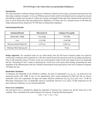
Final Simulated Results:
Simulated Results Microstrip TL Coplanar Waveguide
Bandwidth (-10dB) Very High 76.8 GHz
Loss -2.415 dB -5.445 dB
Minimum Metal Width (W) 6.187 um 8.038 um
Minimum Metal Spacing (G) - 10 um
Design Approach: The simulated results for our initial design from the EM layout extracted symbol was tested by
constructing a testbench which comprised of a 100 ohm resistor between the open ports and also by adding terminations.
Next we fine-tuned the values of W and L (in the case of microstrip) in order to look at the impact it has to our bandwidth
and loss. Decreasing W and L results in decreasing the overall area of the layout while keeping maintaining the same
impedance of the different parts of the line. Similarly decreasing the metal spacing (G) in the case of coplanar waveguide,
will reduce the area.
Bandwidth Calculation:
To determine the bandwidth of the Wilkinson combiner, the plots of S-parameters, , , , are observed at the
intersection points with -10dB. In fact we can appropriately select certain attenuation (in dB) such that we observe
bandwidth. Since the S parameters for input and output reflection coefficients ( , , never cross -10 dB for
Microstrip Transmission Line, its bandwidth cannot be ascertained. However, if we select -18 dB compression for all
three reflection coefficients, we can estimate bandwidth.
Power Loss Calculation:
The total power loss is calculated by adding the magnitude of insertion loss, isolation loss and the return loss in the
combiner. This is calculated at the center frequency for each case. Using the following equation.
Loss
Testbench for extracted EM simulation:
A. A single-ended 30GHz Wilkinson Combiner using a mircrostrip transmission line.
Schematic:
Layout:
Simulations for loss and bandwidth from extracted EM simulation for Microstrip Transmission Line:
Discussion
To increase the bandwidth, the number of input ports could be increased; stepped multiple sections (Pozar). Increasing
numbers of input ports leads to high power loss, which implies larger bandwidth. Area could be further decreased by
decreasing the length of each MLIN. This could be done by decreasing the angle while for the same line impedance by
performing lincalc.
B. A single-ended 60GHz Wilkinson Combiner using a coplanar waveguide transmission line.
Schematic
Layout
Simulations for loss and bandwidth
Discussion
In order to further decrease the area, the metal spacing can be reduced. As a result our bandwidth will increase. In
addition we can increase the bandwidth with a series of coupling holes (Pozar) ie. By increasing the number of input
coupling ports. By reducing the phase of the input CPWGs we can reduce the length of the transmission line for the same
impedance which reduces the area.
References:
(1) Pozar

Contenu connexe

Tendances

Two stage op amp design on cadence
Two stage op amp design on cadenceTwo stage op amp design on cadence
Two stage op amp design on cadenceHaowei Jiang
 
Single Stage Differential Folded Cascode Amplifier
Single Stage Differential Folded Cascode AmplifierSingle Stage Differential Folded Cascode Amplifier
Single Stage Differential Folded Cascode AmplifierAalay Kapadia
 
Low Noise Amplifier at 2 GHz using the transistor NE85639 in ADS
Low Noise Amplifier at 2 GHz using the transistor NE85639 in ADSLow Noise Amplifier at 2 GHz using the transistor NE85639 in ADS
Low Noise Amplifier at 2 GHz using the transistor NE85639 in ADSKarthik Rathinavel
 
Modulation technology
Modulation technologyModulation technology
Modulation technologyPei-Che Chang
 
Theoretic and experimental investigation of gyro-BWO
Theoretic and experimental investigation of gyro-BWOTheoretic and experimental investigation of gyro-BWO
Theoretic and experimental investigation of gyro-BWOPei-Che Chang
 
Lecture psk qam, digital modulation
Lecture psk qam, digital modulation Lecture psk qam, digital modulation
Lecture psk qam, digital modulation DrAimalKhan
 
M-ary Modulation, noise modelling, bandwidth, Bandpass Modulation
M-ary Modulation, noise modelling, bandwidth, Bandpass ModulationM-ary Modulation, noise modelling, bandwidth, Bandpass Modulation
M-ary Modulation, noise modelling, bandwidth, Bandpass ModulationDrAimalKhan
 
Double feedback technique for reduction of Noise LNA with gain enhancement
Double feedback technique for reduction of Noise LNA with gain enhancementDouble feedback technique for reduction of Noise LNA with gain enhancement
Double feedback technique for reduction of Noise LNA with gain enhancementijceronline
 
Communicationlabmanual
CommunicationlabmanualCommunicationlabmanual
Communicationlabmanualjkanth26
 
Impedance matching in awr
Impedance matching in awrImpedance matching in awr
Impedance matching in awrAntul Kashyap
 
DESIGNED A 350NM TWO STAGE OPERATIONAL AMPLIFIER
DESIGNED A 350NM TWO STAGE OPERATIONAL AMPLIFIERDESIGNED A 350NM TWO STAGE OPERATIONAL AMPLIFIER
DESIGNED A 350NM TWO STAGE OPERATIONAL AMPLIFIERIlango Jeyasubramanian
 
RC Circuit Transfer Functions with Bode Diagrams
RC Circuit Transfer Functions with Bode Diagrams RC Circuit Transfer Functions with Bode Diagrams
RC Circuit Transfer Functions with Bode Diagrams Katrina Little
 
RF Power Amplifier Tutorial (1)
RF Power Amplifier Tutorial (1)RF Power Amplifier Tutorial (1)
RF Power Amplifier Tutorial (1)Seong-Hun Choe
 
Digital modulation techniques
Digital modulation techniquesDigital modulation techniques
Digital modulation techniquessrkrishna341
 

Tendances (20)

Ece523 folded cascode design
Ece523 folded cascode designEce523 folded cascode design
Ece523 folded cascode design
 
Two stage op amp design on cadence
Two stage op amp design on cadenceTwo stage op amp design on cadence
Two stage op amp design on cadence
 
Single Stage Differential Folded Cascode Amplifier
Single Stage Differential Folded Cascode AmplifierSingle Stage Differential Folded Cascode Amplifier
Single Stage Differential Folded Cascode Amplifier
 
Folded cascode1
Folded cascode1Folded cascode1
Folded cascode1
 
analog pro.pptx
analog pro.pptxanalog pro.pptx
analog pro.pptx
 
Low Noise Amplifier at 2 GHz using the transistor NE85639 in ADS
Low Noise Amplifier at 2 GHz using the transistor NE85639 in ADSLow Noise Amplifier at 2 GHz using the transistor NE85639 in ADS
Low Noise Amplifier at 2 GHz using the transistor NE85639 in ADS
 
LnA Design_group5
LnA Design_group5LnA Design_group5
LnA Design_group5
 
Modulation technology
Modulation technologyModulation technology
Modulation technology
 
Theoretic and experimental investigation of gyro-BWO
Theoretic and experimental investigation of gyro-BWOTheoretic and experimental investigation of gyro-BWO
Theoretic and experimental investigation of gyro-BWO
 
ECNG 3013 B
ECNG 3013 BECNG 3013 B
ECNG 3013 B
 
Lecture psk qam, digital modulation
Lecture psk qam, digital modulation Lecture psk qam, digital modulation
Lecture psk qam, digital modulation
 
M-ary Modulation, noise modelling, bandwidth, Bandpass Modulation
M-ary Modulation, noise modelling, bandwidth, Bandpass ModulationM-ary Modulation, noise modelling, bandwidth, Bandpass Modulation
M-ary Modulation, noise modelling, bandwidth, Bandpass Modulation
 
Double feedback technique for reduction of Noise LNA with gain enhancement
Double feedback technique for reduction of Noise LNA with gain enhancementDouble feedback technique for reduction of Noise LNA with gain enhancement
Double feedback technique for reduction of Noise LNA with gain enhancement
 
Communicationlabmanual
CommunicationlabmanualCommunicationlabmanual
Communicationlabmanual
 
Impedance matching in awr
Impedance matching in awrImpedance matching in awr
Impedance matching in awr
 
DESIGNED A 350NM TWO STAGE OPERATIONAL AMPLIFIER
DESIGNED A 350NM TWO STAGE OPERATIONAL AMPLIFIERDESIGNED A 350NM TWO STAGE OPERATIONAL AMPLIFIER
DESIGNED A 350NM TWO STAGE OPERATIONAL AMPLIFIER
 
RC Circuit Transfer Functions with Bode Diagrams
RC Circuit Transfer Functions with Bode Diagrams RC Circuit Transfer Functions with Bode Diagrams
RC Circuit Transfer Functions with Bode Diagrams
 
RF Power Amplifier Tutorial (1)
RF Power Amplifier Tutorial (1)RF Power Amplifier Tutorial (1)
RF Power Amplifier Tutorial (1)
 
Digital modulation techniques
Digital modulation techniquesDigital modulation techniques
Digital modulation techniques
 
Group no 11
Group no 11Group no 11
Group no 11
 

Similaire à Ece593 project1 chien_chun_yao_and_karthikvel_rathinavel

Project_Kaveh & Mohammad
Project_Kaveh & MohammadProject_Kaveh & Mohammad
Project_Kaveh & MohammadKaveh Dehno
 
Design of a Low Noise Amplifier using 0.18μm CMOS technology
Design of a Low Noise Amplifier using 0.18μm CMOS technologyDesign of a Low Noise Amplifier using 0.18μm CMOS technology
Design of a Low Noise Amplifier using 0.18μm CMOS technologytheijes
 
Physical designing of low power operational amplifier
Physical designing of low power operational amplifierPhysical designing of low power operational amplifier
Physical designing of low power operational amplifierDevendra Kushwaha
 
Design of Two CMOS Differential Amplifiers
Design of Two CMOS Differential AmplifiersDesign of Two CMOS Differential Amplifiers
Design of Two CMOS Differential Amplifiersbastrikov
 
Distortion Analysis of Differential Amplifier
Distortion Analysis of Differential AmplifierDistortion Analysis of Differential Amplifier
Distortion Analysis of Differential AmplifierIOSR Journals
 
DESIGN AND ANALYSIS OF 2 GHz 130nm CMOS CASCODE LOW NOISE AMPLIFIER WITH INTE...
DESIGN AND ANALYSIS OF 2 GHz 130nm CMOS CASCODE LOW NOISE AMPLIFIER WITH INTE...DESIGN AND ANALYSIS OF 2 GHz 130nm CMOS CASCODE LOW NOISE AMPLIFIER WITH INTE...
DESIGN AND ANALYSIS OF 2 GHz 130nm CMOS CASCODE LOW NOISE AMPLIFIER WITH INTE...csijjournal
 
Design and Implementation of LNA at 900MHz for GSM applications
Design and Implementation of LNA at 900MHz for GSM applicationsDesign and Implementation of LNA at 900MHz for GSM applications
Design and Implementation of LNA at 900MHz for GSM applicationsAbdus Sami
 
Non-radiative wireless energy transfer with single layer dual-band printed sp...
Non-radiative wireless energy transfer with single layer dual-band printed sp...Non-radiative wireless energy transfer with single layer dual-band printed sp...
Non-radiative wireless energy transfer with single layer dual-band printed sp...journalBEEI
 
A LOW POWER, LOW PHASE NOISE CMOS LC OSCILLATOR
A LOW POWER, LOW PHASE NOISE CMOS LC OSCILLATORA LOW POWER, LOW PHASE NOISE CMOS LC OSCILLATOR
A LOW POWER, LOW PHASE NOISE CMOS LC OSCILLATORIJEEE
 
A LOW POWER, LOW PHASE NOISE CMOS LC OSCILLATOR
A LOW POWER, LOW PHASE NOISE CMOS LC OSCILLATORA LOW POWER, LOW PHASE NOISE CMOS LC OSCILLATOR
A LOW POWER, LOW PHASE NOISE CMOS LC OSCILLATORIJEEE
 
An operational amplifier with recycling folded cascode topology and adaptive ...
An operational amplifier with recycling folded cascode topology and adaptive ...An operational amplifier with recycling folded cascode topology and adaptive ...
An operational amplifier with recycling folded cascode topology and adaptive ...VLSICS Design
 
Design of CMOS operational Amplifiers using CADENCE
Design of CMOS operational Amplifiers using CADENCEDesign of CMOS operational Amplifiers using CADENCE
Design of CMOS operational Amplifiers using CADENCEnandivashishth
 
200 m hz flash adc
200 m hz flash adc200 m hz flash adc
200 m hz flash adcVũ Đình
 
HFSS ANTENNA FOR KU BAND WITH DEFECTED GROUND STRUCTURES
HFSS ANTENNA FOR KU BAND WITH DEFECTED GROUND STRUCTURESHFSS ANTENNA FOR KU BAND WITH DEFECTED GROUND STRUCTURES
HFSS ANTENNA FOR KU BAND WITH DEFECTED GROUND STRUCTURESAKSHAT GANGWAR
 
Design and Realization of 2.4GHz Branch-line Coupler
Design and Realization of 2.4GHz Branch-line CouplerDesign and Realization of 2.4GHz Branch-line Coupler
Design and Realization of 2.4GHz Branch-line CouplerQuang Binh Pham
 
A new precision peak detector full wave rectifier
A new precision peak detector full wave rectifierA new precision peak detector full wave rectifier
A new precision peak detector full wave rectifierVishal kakade
 

Similaire à Ece593 project1 chien_chun_yao_and_karthikvel_rathinavel (20)

Project_Kaveh & Mohammad
Project_Kaveh & MohammadProject_Kaveh & Mohammad
Project_Kaveh & Mohammad
 
5992-1632.docx
5992-1632.docx5992-1632.docx
5992-1632.docx
 
Design of a Low Noise Amplifier using 0.18μm CMOS technology
Design of a Low Noise Amplifier using 0.18μm CMOS technologyDesign of a Low Noise Amplifier using 0.18μm CMOS technology
Design of a Low Noise Amplifier using 0.18μm CMOS technology
 
Physical designing of low power operational amplifier
Physical designing of low power operational amplifierPhysical designing of low power operational amplifier
Physical designing of low power operational amplifier
 
Design of Two CMOS Differential Amplifiers
Design of Two CMOS Differential AmplifiersDesign of Two CMOS Differential Amplifiers
Design of Two CMOS Differential Amplifiers
 
July 24, 2003
July 24, 2003July 24, 2003
July 24, 2003
 
Distortion Analysis of Differential Amplifier
Distortion Analysis of Differential AmplifierDistortion Analysis of Differential Amplifier
Distortion Analysis of Differential Amplifier
 
H010235358
H010235358H010235358
H010235358
 
DESIGN AND ANALYSIS OF 2 GHz 130nm CMOS CASCODE LOW NOISE AMPLIFIER WITH INTE...
DESIGN AND ANALYSIS OF 2 GHz 130nm CMOS CASCODE LOW NOISE AMPLIFIER WITH INTE...DESIGN AND ANALYSIS OF 2 GHz 130nm CMOS CASCODE LOW NOISE AMPLIFIER WITH INTE...
DESIGN AND ANALYSIS OF 2 GHz 130nm CMOS CASCODE LOW NOISE AMPLIFIER WITH INTE...
 
Design and Implementation of LNA at 900MHz for GSM applications
Design and Implementation of LNA at 900MHz for GSM applicationsDesign and Implementation of LNA at 900MHz for GSM applications
Design and Implementation of LNA at 900MHz for GSM applications
 
Non-radiative wireless energy transfer with single layer dual-band printed sp...
Non-radiative wireless energy transfer with single layer dual-band printed sp...Non-radiative wireless energy transfer with single layer dual-band printed sp...
Non-radiative wireless energy transfer with single layer dual-band printed sp...
 
A LOW POWER, LOW PHASE NOISE CMOS LC OSCILLATOR
A LOW POWER, LOW PHASE NOISE CMOS LC OSCILLATORA LOW POWER, LOW PHASE NOISE CMOS LC OSCILLATOR
A LOW POWER, LOW PHASE NOISE CMOS LC OSCILLATOR
 
A LOW POWER, LOW PHASE NOISE CMOS LC OSCILLATOR
A LOW POWER, LOW PHASE NOISE CMOS LC OSCILLATORA LOW POWER, LOW PHASE NOISE CMOS LC OSCILLATOR
A LOW POWER, LOW PHASE NOISE CMOS LC OSCILLATOR
 
Ehv line design
Ehv line designEhv line design
Ehv line design
 
An operational amplifier with recycling folded cascode topology and adaptive ...
An operational amplifier with recycling folded cascode topology and adaptive ...An operational amplifier with recycling folded cascode topology and adaptive ...
An operational amplifier with recycling folded cascode topology and adaptive ...
 
Design of CMOS operational Amplifiers using CADENCE
Design of CMOS operational Amplifiers using CADENCEDesign of CMOS operational Amplifiers using CADENCE
Design of CMOS operational Amplifiers using CADENCE
 
200 m hz flash adc
200 m hz flash adc200 m hz flash adc
200 m hz flash adc
 
HFSS ANTENNA FOR KU BAND WITH DEFECTED GROUND STRUCTURES
HFSS ANTENNA FOR KU BAND WITH DEFECTED GROUND STRUCTURESHFSS ANTENNA FOR KU BAND WITH DEFECTED GROUND STRUCTURES
HFSS ANTENNA FOR KU BAND WITH DEFECTED GROUND STRUCTURES
 
Design and Realization of 2.4GHz Branch-line Coupler
Design and Realization of 2.4GHz Branch-line CouplerDesign and Realization of 2.4GHz Branch-line Coupler
Design and Realization of 2.4GHz Branch-line Coupler
 
A new precision peak detector full wave rectifier
A new precision peak detector full wave rectifierA new precision peak detector full wave rectifier
A new precision peak detector full wave rectifier
 

Plus de Karthik Rathinavel

Digital Voltmeter displaying voltage level on a seven segment display and com...
Digital Voltmeter displaying voltage level on a seven segment display and com...Digital Voltmeter displaying voltage level on a seven segment display and com...
Digital Voltmeter displaying voltage level on a seven segment display and com...Karthik Rathinavel
 
Sine Wave Generator with controllable frequency displayed on a seven segment ...
Sine Wave Generator with controllable frequency displayed on a seven segment ...Sine Wave Generator with controllable frequency displayed on a seven segment ...
Sine Wave Generator with controllable frequency displayed on a seven segment ...Karthik Rathinavel
 
Continuous Low Pass Filter Realization using Cascaded stages of Tow-Thomas Bi...
Continuous Low Pass Filter Realization using Cascaded stages of Tow-Thomas Bi...Continuous Low Pass Filter Realization using Cascaded stages of Tow-Thomas Bi...
Continuous Low Pass Filter Realization using Cascaded stages of Tow-Thomas Bi...Karthik Rathinavel
 
Transmitting Digital Signal through Light Pulses
Transmitting Digital Signal through Light PulsesTransmitting Digital Signal through Light Pulses
Transmitting Digital Signal through Light PulsesKarthik Rathinavel
 

Plus de Karthik Rathinavel (6)

Digital Voltmeter displaying voltage level on a seven segment display and com...
Digital Voltmeter displaying voltage level on a seven segment display and com...Digital Voltmeter displaying voltage level on a seven segment display and com...
Digital Voltmeter displaying voltage level on a seven segment display and com...
 
Sine Wave Generator with controllable frequency displayed on a seven segment ...
Sine Wave Generator with controllable frequency displayed on a seven segment ...Sine Wave Generator with controllable frequency displayed on a seven segment ...
Sine Wave Generator with controllable frequency displayed on a seven segment ...
 
Continuous Low Pass Filter Realization using Cascaded stages of Tow-Thomas Bi...
Continuous Low Pass Filter Realization using Cascaded stages of Tow-Thomas Bi...Continuous Low Pass Filter Realization using Cascaded stages of Tow-Thomas Bi...
Continuous Low Pass Filter Realization using Cascaded stages of Tow-Thomas Bi...
 
Transmitting Digital Signal through Light Pulses
Transmitting Digital Signal through Light PulsesTransmitting Digital Signal through Light Pulses
Transmitting Digital Signal through Light Pulses
 
Project Report
Project Report Project Report
Project Report
 
Project presentation
Project presentationProject presentation
Project presentation
 

Dernier

Work Experience-Dalton Park.pptxfvvvvvvv
Work Experience-Dalton Park.pptxfvvvvvvvWork Experience-Dalton Park.pptxfvvvvvvv
Work Experience-Dalton Park.pptxfvvvvvvvLewisJB
 
What are the advantages and disadvantages of membrane structures.pptx
What are the advantages and disadvantages of membrane structures.pptxWhat are the advantages and disadvantages of membrane structures.pptx
What are the advantages and disadvantages of membrane structures.pptxwendy cai
 
Application of Residue Theorem to evaluate real integrations.pptx
Application of Residue Theorem to evaluate real integrations.pptxApplication of Residue Theorem to evaluate real integrations.pptx
Application of Residue Theorem to evaluate real integrations.pptx959SahilShah
 
Concrete Mix Design - IS 10262-2019 - .pptx
Concrete Mix Design - IS 10262-2019 - .pptxConcrete Mix Design - IS 10262-2019 - .pptx
Concrete Mix Design - IS 10262-2019 - .pptxKartikeyaDwivedi3
 
Instrumentation, measurement and control of bio process parameters ( Temperat...
Instrumentation, measurement and control of bio process parameters ( Temperat...Instrumentation, measurement and control of bio process parameters ( Temperat...
Instrumentation, measurement and control of bio process parameters ( Temperat...121011101441
 
An introduction to Semiconductor and its types.pptx
An introduction to Semiconductor and its types.pptxAn introduction to Semiconductor and its types.pptx
An introduction to Semiconductor and its types.pptxPurva Nikam
 
Past, Present and Future of Generative AI
Past, Present and Future of Generative AIPast, Present and Future of Generative AI
Past, Present and Future of Generative AIabhishek36461
 
Call Girls Narol 7397865700 Independent Call Girls
Call Girls Narol 7397865700 Independent Call GirlsCall Girls Narol 7397865700 Independent Call Girls
Call Girls Narol 7397865700 Independent Call Girlsssuser7cb4ff
 
Risk Assessment For Installation of Drainage Pipes.pdf
Risk Assessment For Installation of Drainage Pipes.pdfRisk Assessment For Installation of Drainage Pipes.pdf
Risk Assessment For Installation of Drainage Pipes.pdfROCENODodongVILLACER
 
Introduction-To-Agricultural-Surveillance-Rover.pptx
Introduction-To-Agricultural-Surveillance-Rover.pptxIntroduction-To-Agricultural-Surveillance-Rover.pptx
Introduction-To-Agricultural-Surveillance-Rover.pptxk795866
 
An experimental study in using natural admixture as an alternative for chemic...
An experimental study in using natural admixture as an alternative for chemic...An experimental study in using natural admixture as an alternative for chemic...
An experimental study in using natural admixture as an alternative for chemic...Chandu841456
 
Gurgaon ✡️9711147426✨Call In girls Gurgaon Sector 51 escort service
Gurgaon ✡️9711147426✨Call In girls Gurgaon Sector 51 escort serviceGurgaon ✡️9711147426✨Call In girls Gurgaon Sector 51 escort service
Gurgaon ✡️9711147426✨Call In girls Gurgaon Sector 51 escort servicejennyeacort
 
Gfe Mayur Vihar Call Girls Service WhatsApp -> 9999965857 Available 24x7 ^ De...
Gfe Mayur Vihar Call Girls Service WhatsApp -> 9999965857 Available 24x7 ^ De...Gfe Mayur Vihar Call Girls Service WhatsApp -> 9999965857 Available 24x7 ^ De...
Gfe Mayur Vihar Call Girls Service WhatsApp -> 9999965857 Available 24x7 ^ De...srsj9000
 
CCS355 Neural Network & Deep Learning Unit II Notes with Question bank .pdf
CCS355 Neural Network & Deep Learning Unit II Notes with Question bank .pdfCCS355 Neural Network & Deep Learning Unit II Notes with Question bank .pdf
CCS355 Neural Network & Deep Learning Unit II Notes with Question bank .pdfAsst.prof M.Gokilavani
 
UNIT III ANALOG ELECTRONICS (BASIC ELECTRONICS)
UNIT III ANALOG ELECTRONICS (BASIC ELECTRONICS)UNIT III ANALOG ELECTRONICS (BASIC ELECTRONICS)
UNIT III ANALOG ELECTRONICS (BASIC ELECTRONICS)Dr SOUNDIRARAJ N
 
Architect Hassan Khalil Portfolio for 2024
Architect Hassan Khalil Portfolio for 2024Architect Hassan Khalil Portfolio for 2024
Architect Hassan Khalil Portfolio for 2024hassan khalil
 
Decoding Kotlin - Your guide to solving the mysterious in Kotlin.pptx
Decoding Kotlin - Your guide to solving the mysterious in Kotlin.pptxDecoding Kotlin - Your guide to solving the mysterious in Kotlin.pptx
Decoding Kotlin - Your guide to solving the mysterious in Kotlin.pptxJoão Esperancinha
 

Dernier (20)

Work Experience-Dalton Park.pptxfvvvvvvv
Work Experience-Dalton Park.pptxfvvvvvvvWork Experience-Dalton Park.pptxfvvvvvvv
Work Experience-Dalton Park.pptxfvvvvvvv
 
What are the advantages and disadvantages of membrane structures.pptx
What are the advantages and disadvantages of membrane structures.pptxWhat are the advantages and disadvantages of membrane structures.pptx
What are the advantages and disadvantages of membrane structures.pptx
 
Application of Residue Theorem to evaluate real integrations.pptx
Application of Residue Theorem to evaluate real integrations.pptxApplication of Residue Theorem to evaluate real integrations.pptx
Application of Residue Theorem to evaluate real integrations.pptx
 
Concrete Mix Design - IS 10262-2019 - .pptx
Concrete Mix Design - IS 10262-2019 - .pptxConcrete Mix Design - IS 10262-2019 - .pptx
Concrete Mix Design - IS 10262-2019 - .pptx
 
Instrumentation, measurement and control of bio process parameters ( Temperat...
Instrumentation, measurement and control of bio process parameters ( Temperat...Instrumentation, measurement and control of bio process parameters ( Temperat...
Instrumentation, measurement and control of bio process parameters ( Temperat...
 
young call girls in Rajiv Chowk🔝 9953056974 🔝 Delhi escort Service
young call girls in Rajiv Chowk🔝 9953056974 🔝 Delhi escort Serviceyoung call girls in Rajiv Chowk🔝 9953056974 🔝 Delhi escort Service
young call girls in Rajiv Chowk🔝 9953056974 🔝 Delhi escort Service
 
An introduction to Semiconductor and its types.pptx
An introduction to Semiconductor and its types.pptxAn introduction to Semiconductor and its types.pptx
An introduction to Semiconductor and its types.pptx
 
Past, Present and Future of Generative AI
Past, Present and Future of Generative AIPast, Present and Future of Generative AI
Past, Present and Future of Generative AI
 
9953056974 Call Girls In South Ex, Escorts (Delhi) NCR.pdf
9953056974 Call Girls In South Ex, Escorts (Delhi) NCR.pdf9953056974 Call Girls In South Ex, Escorts (Delhi) NCR.pdf
9953056974 Call Girls In South Ex, Escorts (Delhi) NCR.pdf
 
young call girls in Green Park🔝 9953056974 🔝 escort Service
young call girls in Green Park🔝 9953056974 🔝 escort Serviceyoung call girls in Green Park🔝 9953056974 🔝 escort Service
young call girls in Green Park🔝 9953056974 🔝 escort Service
 
Call Girls Narol 7397865700 Independent Call Girls
Call Girls Narol 7397865700 Independent Call GirlsCall Girls Narol 7397865700 Independent Call Girls
Call Girls Narol 7397865700 Independent Call Girls
 
Risk Assessment For Installation of Drainage Pipes.pdf
Risk Assessment For Installation of Drainage Pipes.pdfRisk Assessment For Installation of Drainage Pipes.pdf
Risk Assessment For Installation of Drainage Pipes.pdf
 
Introduction-To-Agricultural-Surveillance-Rover.pptx
Introduction-To-Agricultural-Surveillance-Rover.pptxIntroduction-To-Agricultural-Surveillance-Rover.pptx
Introduction-To-Agricultural-Surveillance-Rover.pptx
 
An experimental study in using natural admixture as an alternative for chemic...
An experimental study in using natural admixture as an alternative for chemic...An experimental study in using natural admixture as an alternative for chemic...
An experimental study in using natural admixture as an alternative for chemic...
 
Gurgaon ✡️9711147426✨Call In girls Gurgaon Sector 51 escort service
Gurgaon ✡️9711147426✨Call In girls Gurgaon Sector 51 escort serviceGurgaon ✡️9711147426✨Call In girls Gurgaon Sector 51 escort service
Gurgaon ✡️9711147426✨Call In girls Gurgaon Sector 51 escort service
 
Gfe Mayur Vihar Call Girls Service WhatsApp -> 9999965857 Available 24x7 ^ De...
Gfe Mayur Vihar Call Girls Service WhatsApp -> 9999965857 Available 24x7 ^ De...Gfe Mayur Vihar Call Girls Service WhatsApp -> 9999965857 Available 24x7 ^ De...
Gfe Mayur Vihar Call Girls Service WhatsApp -> 9999965857 Available 24x7 ^ De...
 
CCS355 Neural Network & Deep Learning Unit II Notes with Question bank .pdf
CCS355 Neural Network & Deep Learning Unit II Notes with Question bank .pdfCCS355 Neural Network & Deep Learning Unit II Notes with Question bank .pdf
CCS355 Neural Network & Deep Learning Unit II Notes with Question bank .pdf
 
UNIT III ANALOG ELECTRONICS (BASIC ELECTRONICS)
UNIT III ANALOG ELECTRONICS (BASIC ELECTRONICS)UNIT III ANALOG ELECTRONICS (BASIC ELECTRONICS)
UNIT III ANALOG ELECTRONICS (BASIC ELECTRONICS)
 
Architect Hassan Khalil Portfolio for 2024
Architect Hassan Khalil Portfolio for 2024Architect Hassan Khalil Portfolio for 2024
Architect Hassan Khalil Portfolio for 2024
 
Decoding Kotlin - Your guide to solving the mysterious in Kotlin.pptx
Decoding Kotlin - Your guide to solving the mysterious in Kotlin.pptxDecoding Kotlin - Your guide to solving the mysterious in Kotlin.pptx
Decoding Kotlin - Your guide to solving the mysterious in Kotlin.pptx
 

Ece593 project1 chien_chun_yao_and_karthikvel_rathinavel

  • 1. ECE 593 Project 1 By: Chien Chun Yao and Karthikvel Rathinavel Introduction: This report describes a method to design and layout a Wilkinson combiner by first using a microstip transmission line and then using a coplanar waveguide. A two way Wilkinson power divider works by dividing the power coming from one port and splitting it equally into two parts if it splits into a quarter wavelength in both sides and a shunted resistor between the ports. It can be shown that if the input characteristic impedance is 50 ohms, then for a shunted resistor of 100 ohms the output transmission lines should have 70.7106 ohms of characteristic impedance. Final Simulated Results: Simulated Results Microstrip TL Coplanar Waveguide Bandwidth (-10dB) Very High 76.8 GHz Loss -2.415 dB -5.445 dB Minimum Metal Width (W) 6.187 um 8.038 um Minimum Metal Spacing (G) - 10 um Design Approach: The simulated results for our initial design from the EM layout extracted symbol was tested by constructing a testbench which comprised of a 100 ohm resistor between the open ports and also by adding terminations. Next we fine-tuned the values of W and L (in the case of microstrip) in order to look at the impact it has to our bandwidth and loss. Decreasing W and L results in decreasing the overall area of the layout while keeping maintaining the same impedance of the different parts of the line. Similarly decreasing the metal spacing (G) in the case of coplanar waveguide, will reduce the area. Bandwidth Calculation: To determine the bandwidth of the Wilkinson combiner, the plots of S-parameters, , , , are observed at the intersection points with -10dB. In fact we can appropriately select certain attenuation (in dB) such that we observe bandwidth. Since the S parameters for input and output reflection coefficients ( , , never cross -10 dB for Microstrip Transmission Line, its bandwidth cannot be ascertained. However, if we select -18 dB compression for all three reflection coefficients, we can estimate bandwidth. Power Loss Calculation: The total power loss is calculated by adding the magnitude of insertion loss, isolation loss and the return loss in the combiner. This is calculated at the center frequency for each case. Using the following equation. Loss
  • 2. Testbench for extracted EM simulation:
  • 3. A. A single-ended 30GHz Wilkinson Combiner using a mircrostrip transmission line. Schematic: Layout:
  • 4. Simulations for loss and bandwidth from extracted EM simulation for Microstrip Transmission Line: Discussion To increase the bandwidth, the number of input ports could be increased; stepped multiple sections (Pozar). Increasing numbers of input ports leads to high power loss, which implies larger bandwidth. Area could be further decreased by decreasing the length of each MLIN. This could be done by decreasing the angle while for the same line impedance by performing lincalc.
  • 5. B. A single-ended 60GHz Wilkinson Combiner using a coplanar waveguide transmission line. Schematic Layout
  • 6. Simulations for loss and bandwidth Discussion In order to further decrease the area, the metal spacing can be reduced. As a result our bandwidth will increase. In addition we can increase the bandwidth with a series of coupling holes (Pozar) ie. By increasing the number of input coupling ports. By reducing the phase of the input CPWGs we can reduce the length of the transmission line for the same impedance which reduces the area. References: (1) Pozar