

Recommandé
Recommandé
Contenu connexe
Tendances
Tendances (19)
Similaire à Ultrasparc3 (mpr)
Similaire à Ultrasparc3 (mpr) (20)
Plus de Léia de Sousa
Plus de Léia de Sousa (10)
Dernier
Dernier (20)
Ultrasparc3 (mpr)
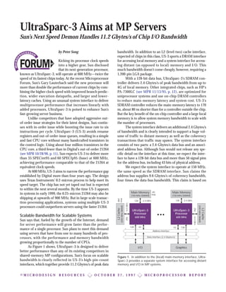
- 1. © M I C R O D E S I G N R E S O U R C E S O C T O B E R 2 7 , 1 9 9 7 M I C R O P R O C E S S O R R E P O R T by Peter Song Kicking its processor clock speeds into a higher gear, Sun disclosed that its next-generation processor, known as UltraSparc-3, will operate at 600 MHz—twice the speed of its fastest chips today. At the recent Microprocessor Forum, Sun’s Gary Lauterbach said the new processor will more than double the performance of current chips by com- bining the higher clock speed with improved branch predic- tion, wider execution datapaths, and larger and lower- latency caches. Using an unusual system interface to deliver multiprocessor performance that increases linearly with added processors, UltraSparc-3 is poised to enhance Sun’s fast-growing server business. Unlike competitors that have adopted aggressive out- of-order issue strategies for their latest designs, Sun contin- ues with in-order issue while boosting the issue rate to six instructions per cycle. UltraSparc-3 (US-3) avoids rename registers and out-of-order-issue queues, resulting in a simple and fast CPU core without many handcrafted transistors in the control logic. Using about four million transistors in the CPU core, a third fewer than in Digital’s out-of-order 21264 (see MPR 10/28/96, p. 11), Sun expects US-3 to deliver more than 35 SPECint95 and 60 SPECfp95 (base) at 600 MHz, achieving performance comparable to that of the 21264 at equivalent clock speeds. At 600 MHz, US-3 aims to narrow the performance gap established by Digital more than four years ago. The design uses Texas Instruments’ 0.2-micron process to help meet its speed target. The chip has not yet taped out but is expected to within the next several months. By the time US-3 appears in systems in early 1999, the 0.25-micron 21264 may also be shipping at upwards of 900 MHz. But in large-scale transac- tion-processing applications, systems using multiple US-3 processors could outperform servers using the faster 21264. Scalable Bandwidth for Scalable Systems Sun says that, fueled by the growth of the Internet, demand for server performance will grow faster than the perfor- mance of a single processor. Sun plans to meet this demand using servers that have from one to many hundreds of pro- cessors, with the performance and memory bandwidth growing proportionally to the number of CPUs. As Figure 1 shows, UltraSparc-3 is designed to deliver better performance than any of its existing competitors in shared-memory MP configurations. Sun’s focus on scalable bandwidth is clearly reflected in US-3’s high-pin-count interfaces, which together provide 11.2 Gbytes/s of peak data bandwidth. In addition to an L2 (level-two) cache interface, expected of chips in this class, US-3 sports a DRAM interface for accessing local memory and a system interface for access- ing distant (as opposed to local) memory and I/O. This much bandwidth doesn’t come cheaply, however, requiring a 1,200-pin LGA package. With a 128-bit data bus, UltraSparc-3’s SDRAM con- troller delivers 2.4 Gbytes/s of peak bandwidth from up to 4G of local memory. Other integrated chips, such as HP’s PA-7300LC (see MPR 11/13/95, p. 12), are optimized for uniprocessor systems and use on-chip DRAM controllers to reduce main-memory latency and system cost. US-3’s SDRAM controller reduces the main-memory latency to 170 ns, about 80 ns shorter than for a controller outside the chip. But the key benefit of the on-chip controller and a large local memory is to allow system memory bandwidth to scale with the number of processors. The system interface delivers an additional 2.4 Gbytes/s of bandwidth and is clearly intended to support a huge vol- ume of traffic to distant memory as well as the coherency transactions that traffic may spawn. The system interface consists of two parts: a 2.4-Gbytes/s data bus and an associ- ated address bus. Although Sun would not release any spe- cific detail on the interface at this time, we expect the inter- face to have a 128-bit data bus and more than 50 signal pins for the address bus, including 43 bits of physical address. We expect the system interface to operate at 150 MHz, the same speed as the SDRAM interface. Sun claims the address bus supplies 9.6 Gbytes/s of coherency bandwidth, four times the data-bus bandwidth. This claim is based on UltraSparc-3 Aims at MP Servers Sun’s Next Speed Demon Handles 11.2 Gbytes/s of Chip I/O Bandwidth Address Interface Main Memory (150-MHz SDRAM) UltraSparc-3 Processor 600 MHz L2Cache (200-MHzSRAM) 128 256 Main Memory (150-MHz SDRAM) L2Cache (200-MHzSRAM) 128 256 UltraSparc-3 Processor 600 MHz 2.4 GB/s 2.4 GB/s 6.4GB/s 6.4GB/s Data Interface (2.4 Gbytes/s) GraphicsI/O 1284343128 8M max 4G max Figure 1. In addition to the (local) main-memory interface, Ultra- Sparc-3 provides a separate system interface for accessing distant memory and I/O in MP systems.
- 2. 2 U LT R A S P A R C - 3 A I M S A T M P S E R V E R S © M I C R O D E S I G N R E S O U R C E S O C T O B E R 2 7 , 1 9 9 7 M I C R O P R O C E S S O R R E P O R T the fact that one coherency transaction covers a cache line of 64 bytes, four times the data-bus width, and that the trans- action may not need a data transfer. Actual data transfers, however, use the data bus, so the 9.6 Gbytes/s does not in any way increase the chip’s data bandwidth. The system interface is designed to support ccNUMA (cache-coherent non-uniform memory access) configura- tions. It supports up to four processors, each of which may or may not have its own local memory, in a shared-bus configuration. A more elaborate interconnect, such as a hierarchy of buses or switches, is needed to support more than four processors. The system interface supports up to 15 outstanding transactions that can complete out of order while maintaining SPARC V9’s TSO (total store order) model. To minimize coherency overhead, the no-snoop attribute is available for each page. On-Chip Tag Array Boosts Coherency Bandwidth Using a 256-bit data bus, UltraSparc-3’s L2-cache interface provides much greater bandwidth than any of its competi- tors’. When using 200-MHz SRAMs, the interface delivers 6.4 Gbytes/s of bandwidth, twice the bandwidth of the 21264’s 128-bit interface using the same SRAMs. Unlike other high-end processors, it incorporates the tag array for the L2 cache, as Figure 2 shows. Bringing the L2 tag array on board offers performance advantages. Because the on-chip tag array is clocked at the CPU speed, not the L2 cache speed, bandwidth available for accessing the tag array is higher and will scale better with increased processor speed. The tag-array must provide enough bandwidth to accommodate not only the proces- sor’s cache accesses but also the large amount of coherency traffic in a multiprocessor system. In addition, because the access to the on-chip tag array is faster, the L2-cache-miss condition is known sooner and, therefore, the main-mem- ory access can start earlier. The faster access also reduces the latency of coherency transactions. Compared with an off- chip tag array built using 200-MHz SRAMs, the on-chip tag array provides three times the bandwidth and reduces the L2-cache-miss latency by 10 cycles, according to Sun. Bringing the tag array on chip is expensive, however, taking 90 Kbytes of SRAM to support up to 8M of L2 cache. The tag array occupies roughly the same area as the 32K L1 instruction cache. It also limits the size of the off-chip cache, although most systems will find the 8M limit more than ade- quate. Since part of the tag array is currently wasted if fewer than 8M are used, an UltraSparc-3 derivative could support a set-associative organization, improving the hit ratio of smaller L2 caches without adding more pins or SRAM. In-Order Issue Keeps Core Simple The core of US-3 executes instructions mostly in program order, at a peak rate of six per cycle and a sustainable rate of four per cycle. The instructions are fetched at most four per cycle and issued to the execution units in the program order. Due to multiple execution units with different numbers of pipeline stages, instructions that are issued in order do not necessarily finish (produce results) in the same order. By supporting out-of-order execution in places where it occurs naturally, US-3 uses relatively simple mechanisms to enforce instruction dependencies and present a precise exception model to software. The instructions are partially decoded and placed into the 20-entry instruction queue, which is modest compared with Dispatch Unit Fetch Unit Instr TLB (128 entries) Data TLB (512 entries) Instruction Cache (32K 4-way associatve) Instr Queue (20 entries) 4 instr 6 instr 256 bits / Cache Control / DRAM Control System Interface Branch Unit Main Data Cache (64K, 4-way) BHT (16K entries) Seq Instr Queue (4 entries) 6 instr FP Adder FP × ÷ √ ALU / Load Load / Store 128bits SDRAM (150 MHz) L2 Cache (200 MHz) Integer ALU Prefetch Cache (2K, 4-way) Write Cache (2K, 4-way) Store Queue (8 entries) L2 Tags Data Bus (150 MHz) Address Bus (150 MHz) 128bits 43bits 256bits 64 64 256 Figure 2. UltraSparc-3 issues six instructions in order into four integer units and two floating-point/graphics units. Mispredicted fall-thru-branch penalty: 3 cycles Calc PC Fetch1 Register ExecuteIssueQueueTargetFetch2 Register Address Cache WriteAlign Register FP1 FP2 FP3 FP4 Trap Commit Extend Mispredicted taken-branch penalty: 7 cycles Target calculation : 2 cycles Load-use penalty: 1 cycle Float, graphics dependency: 4 cycles Decode Figure 3. The 14-stage pipeline simplifies control logic but yields seven cycles of branch-misprediction penalty.
- 3. © M I C R O D E S I G N R E S O U R C E S O C T O B E R 2 7 , 1 9 9 7 M I C R O P R O C E S S O R R E P O R T 3 U LT R A S P A R C - 3 A I M S A T M P S E R V E R S the 56-entry queue in HP’s PA-8000 (see MPR 11/14/94,p.1) or the 21264 chip’s 20-entry integer and 15-entry floating-point instruction queues. Since instructions are issued in order from the queue, unlike in the PA-8000 or the 21264, more than 20 entries would not improve performance significantly on most applications.Wheninstructionsarebeingissuedatthepeakrate of six per cycle, the 20-entry queue can hold enough instruc- tions to last from 4 cycles (when it is not being filled) to more than 10 cycles (when it is being filled at the peak rate). Each cycle, up to six instructions are taken from the queue, decoded, and issued to the execution units. The instructions that are issued in the same cycle form an issue group with appropriate age bits to maintain the instruction order within the group. If an instruction cannot be issued because an operand or the execution unit is not available, it remains in the issue stage, blocking the queue. An exception to this rule: branch instructions are issued before their con- ditions are known, allowing speculative execution of instructions in the predicted paths. Once issued, the instructions in each issue group advance in lockstep, simplify- ing the logic needed to keep track of the program counter and the instruction order within the group. Except for the few nonpipelined instructions, instructions do not stall once they enter the execution pipeline. The should-be-stalled instruc- tions are,instead,fetched and issued again once the pipeline-hold conditions are removed. This avoids a chain of pipeline- hold signals that propagates through mul- tiple stages. Because interconnect delays begin to dominate over gate delays as pro- cess dimensions shrink below 0.25 microns (see MPR 8/4/97, p. 14), US-3 designers avoided features that require signals to traverse long wires in a short time. Deep Fetch Pipeline Avoids Long Wires The designers’ concern for long interconnects and short cycle time is evident in UltraSparc-3’s 14-stage pipeline, longer than that of any RISC processor announced to date. As Figure 3 shows, US-3 has six stages, two more than the 21264, before it executes instructions. It uses eight stages, six more than the 21264, before the integer results are written to the architectural register file, but these extra stages do not degrade performance, since the results are made available to dependent instructions as soon as they are produced. The 32K L1 instruction cache is accessed in two cycles, but its wave-pipelined design allows an access to begin each cycle. Many of HP’s PA-RISC chips, which use multicycle off- chip cache, have used a wave pipeline to launch the address for the next cache access before the data is received from the previous access (see MPR 11/14/94, p. 1). Multicycle caches are a good candidate for the wave-pipeline technique, because it is impractical to place pipeline registers within the cache arrays. For US-3, the propagation delays through the cache always take more than one but less than two cycles. Although the instruction cache is organized as four- way set-associative, microtags minimize the access-time penalty for having the four sets. The cache is accessed with a virtual address to select a group of four lines and the associ- ated four microtags. The microtags, which consist of eight bits of virtual address, are compared with the corresponding eight bits of the fetch address to select the set. The 8-bit microtags keep the tag-array-access and tag-comparison times to 2 ns, the time taken to access the instruction array. Using the physical-address tags, which are 30 bits long, would result in longer array-access and comparison times, making cache access longer than two cycles. Because the microtags use the virtual address and only eight bits of that, a match on a microtag does not guarantee a cache hit. In parallel with the cache access, the 64-bit virtual address is translated to the 43-bit physical address using dual TLBs. The larger TLB contains 128 entries organized into four sets, and the smaller TLB contains only 16 entries that are fully associative. The physical address is com- pared against the full-length tags to deter- mine a cache hit, which becomes known late in the second fetch stage. A group of four instructions can be fetched from any position within a 32-byte line. Some high-speed instruction caches can access only an aligned group of four words to avoid using slow alignment multiplexors in critical paths. Such designs generally do not fetch all four branch-target instructions in a single cycle, except when the branch target is quadword aligned, relying on compilers to align branch targets and improve fetch efficiency. US-3 designers added the align- ment hardware to improve performance of existing SPARC binaries, most of which do not have aligned branch targets. Branch Prediction Compensates for Deep Pipeline The long fetch pipeline could easily cripple UltraSparc-3’s performance if not for its advanced branch prediction. US-3 incurs seven cycles of penalty on mispredicted branches that are taken, but less on those that are not taken, as Figure 3 shows. Assuming one branch every five instructions, a mis- prediction rate of 10% would impose a penalty of 0.14 cycles per instruction (CPI) (7 cycles × 0.2 × 10%) for US-3. Com- pared with its peak throughput of four instructions per cycle (or 0.25 CPI), the 0.14 CPI penalty would degrade the pro- cessor’s performance by 56%. US-3 designers spent much effort to devise a prediction mechanism they believe achieves accuracy at least as good as most of the published algorithms. According to Lauterbach, Gary Lauterbach describes Ultra- Sparc-3’s huge coherency band- width, intended for MP servers. MICHAELMUSTACCHI
- 4. 4 U LT R A S P A R C - 3 A I M S A T M P S E R V E R S © M I C R O D E S I G N R E S O U R C E S O C T O B E R 2 7 , 1 9 9 7 M I C R O P R O C E S S O R R E P O R T the algorithm Sun implemented delivers 95% accuracy on SPEC95, comparable to the two-level adaptive prediction mechanism used in Digital’s 21264 (see MPR 3/27/95, p.17). US-3 uses a one-level 16K-entry predictor that is accessed by hashing 14 bits of branch address and 12 bits of the global branch history. The branch predictor requires 32 Kbits of storage, about the same as the 21264 chip’s 35-Kbit design. Using the SI (sequential instruction) queue, the penalty for mispredicting fall-through branches is reduced from seven to three cycles. The SI queue stores up to four instruc- tions that sequentially follow a predicted-taken branch. When the branch is resolved opposite to its predicted out- come, the instructions kept in the SI queue advance immedi- ately to the issue stage, saving four cycles. The savings may be temporary, however, since the next group of instructions still takes seven cycles to reach the execute stage. Ignoring this effect, Sun claims US-3’s average branch penalty to be 4.5 cycles, or 0.05 CPI, for a mix of 20% branch instructions with 95% branch-prediction accuracy. Unlike other high-performance designs, US-3 does not use a BTB (branch target buffer) and pays a two-cycle “bub- ble” for predicted-taken branches. For US-3, the SI queue is easier to implement than a BTB; the two-cycle gap between fetching a taken branch and fetching its targets gives enough time to fetch instructions in the not-taken path. Like other chips, the processor also includes an eight-entry return- address stack to aid in branch prediction for subroutines. Working Register File Keeps Future State US-3 executes instructions out of order and speculatively using a simple register-renaming scheme. Because instruc- tions are issued in program order, the processor’s pipeline is immune from antidependency (write-after-read) hazards without using rename registers; a later instruction cannot overwrite the register that an earlier instruction has not yet read. Using age bits, the pipeline also avoids output-depen- dency (write-after-write) hazards without the rename regis- ters; an earlier instruction (with a longer latency) is not allowed to overwrite a register that a later instruction (with a shorter latency) has already written. To present a precise-exception model to programs while supporting speculative execution, US-3 uses the WRF (working register file) in addition to the ARF (architectural register file), as Figure 4 shows. The WRF keeps the future state, the result of speculatively executed instructions, while the ARF maintains the architectural state, the state of the pro- cessor that is visible to software. The WRF contains 32 regis- ters that correspond to the current window in the ARF. Integer results are written to the WRF a cycle after they are produced. The results also advance through the pipeline, accompanying the corresponding instructions as they move toward the commit stage. As instructions are retired in the commit stage, their results are written to the ARF in the pro- gram order, making them visible to software when an excep- tion occurs afterwards. If an exception occurs before the instructions are retired, their results are not written to the ARF, preserving the previous state as if the discarded instruc- tions were never executed. To process the exception, the reg- isters in the exception-handler window are copied from the ARF to the WRF, initializing the WRF to the new window. In the register-windowed SPARC architecture, a win- dow switch occurs not only on an exception but, far more frequently, on a call and the return from a subroutine. The window-switch mechanism is also used to restore the WRF after mispredicting a branch, since the WRF is likely to con- tain results of instructions that should not have executed. Using a 2,048-bit bus, US-3 takes only a single cycle to copy a full window from the ARF to the WRF. Execution Datapaths Avoid Stalls The WRF has seven read ports to sustain the peak issue rate of four integer instructions, one of which must be a branch or conditional move, each cycle. The two integer ALUs exe- cute all single-cycle instructions, and the ASU (arithmetic special unit) executes multicycle instructions, such as multi- ply. Either ALU can also calculate the effective address of the prefetch-load instructions, which access only the prefetch cache. These instructions are differentiated from the normal load instructions, which access only the data cache, by a bit in the instruction format. The load, store, and multicycle instructions share the read ports and must be issued one at a time. The results of the ALUs are forwarded to the WRF, so dependent instructions can start without any penalty. The load results are also forwarded to the WRF but, due to their two-cycle latencies, the dependent instructions incur one cycle of load-use latency. When a load instruction encoun- ters an L1 data-cache miss, the instructions that are already in the execute pipeline are allowed to execute while the cache miss is serviced, corrupting the WRF. After restoring the Register Execute Cache2 Align Commit WorkingRegisterFile(32) 2,048 ALU0 ALU Special RegisterFile(8×32) 2 × 64 2 × 64 2 × 64 3 × 64 ALU1 Result forwarding bus WRF Restore bus 64 64 64 64 Store data Architectural GP/FP Add GP Mul/FP Mul, Div, Sqrt 2 × 64 64 64 FP/GP RegisterFile 64 2 × 64 2 × 64 Prefetch Data Ext Figure 4. The results of speculatively executed instructions are kept in the WRF (working register file) and in the registers in each pipeline stage.
- 5. © M I C R O D E S I G N R E S O U R C E S O C T O B E R 2 7 , 1 9 9 7 M I C R O P R O C E S S O R R E P O R T 5 U LT R A S P A R C - 3 A I M S A T M P S E R V E R S WRF, the instruction that incurs the miss and the instruc- tions that follow it are fetched and issued again, in time for the load instruction to hit in the cache. One floating-point (FP) or graphics (GR) add instruc- tion and one FP or GR multiply instruction can be issued each cycle. Both instructions are pipelined and have four- cycle latency, as Table 1 shows. The results of add or multiply instructions are forwarded to the read stage from the trap stage, allowing dependent instructions to execute with only four cycles of latency. In place of a multiply instruction, a nonpipelined FP divide or square-root instruction can be issued. While the result is being computed, instructions that are not depen- dent on it are allowed to execute. In the first few cycles of the divide or square-root calculation, a pessimistic prediction determines if the calculation can result in an exception. This mechanism allows instructions that are later than the divide or square root to update the architectural registers before the divide or the square root retires, resulting in a simple float- ing-point pipeline design. When the prediction is wrong, however, it causes an unnecessary exception. Write Cache Eliminates 90% of L2 Traffic Because it takes so much hardware to undo writes to cache or memory, and the writes to them are generally not urgent, store instructions are not executed speculatively. In Ultra- Sparc-3, store instructions are kept in the eight-entry store queue until they are retired. After a store instruction is retired, its data is written from the store queue to the L1 data cache—if it hits in the data cache—and to the write cache, as Figure 5 shows. Because the data cache uses a write-through policy, it is easier to not update the cache on a miss (known as non-write-allocate) than to reload and update the cache (known as write-allocate). Since the write cache uses a write- back policy, it tends to merge writes to the same lines, updat- ing the L2 cache in larger blocks of writes when it replaces a modified line. The 2K write cache eliminates 90% of the store traffic to the L2 cache, according to Lauterbach. If a load instruction accesses the same address as a store in the store queue, the data is forwarded from the queue, provided that all bytes being read are in the queue. This mechanism, known as store forwarding, is generally provided when an architecture causes programs to write and soon after they read from the same address.An example is the way argu- ments to subroutines are passed—the calling routine pushes the arguments onto a stack and the callee routine pops them—that causes frequent writes followed by reads from the same addresses. For register-window-based US-3, this mech- anism is necessary for multimedia programs that use VIS, the set of multimedia instructions implemented on the floating- point registers (see MPR 12/5/94, p. 16). Because the SPARC architecture does not provide an instruction to directly trans- fer between the integer and floating-point registers, programs are forced to use the cache as an intermediary. SAM Decoder Shortens Data Cache Access The L1 data cache contains 64 Kbytes, organized as four-way set-associative with 32 bytes per line. The data cache is indexed with 9 bits of the virtual address. Instead of using an adder to generate the address, a special decoder uses both the base address and the offset to select one of 512 sets, eliminat- ing one adder delay from the critical cache-access path. This SAM (sum-addressed memory) decoder takes two 9-bit inputs, one from the base address and the other from the off- set, and generates the outputs that are logically equivalent to adding the two inputs and then decoding the sum. Imple- mented in CMOS domino (precharge-evaluate) logic, the SAM decoder completes in only two gate delays. The SAM decoder selects two groups of four lines. The first group is used if the sum of the least-significant five bits of the base address and the offset does not generate a carry. Otherwise, the second group is used. The SAM decoder also accesses the microtags. As in the instruction cache, the microtags select one of the four sets, but the data-cache hit is later confirmed using the physical address. The prefetch cache supports software to better manage cache-miss latency. It supports up to eight software- and hardware-initiated prefetch requests. Using a 256-bit write port, it can fill a 64-byte line in 14 cycles from the L2 cache. In addition, it can service two load instructions simultane- ously with three-cycle latency, one more than the regular data cache. For load instructions that hit in the prefetch cache, it autonomously initiates the prefetch for their next UltraSparc-3 Alpha 21264 Throughput Latency Throughput Latency Integer Multiply Integer Divide Graphics Add/Mul FP Add/Mul FP Divide (SP) FP Square Root (SP) FP Divide (DP) FP Square Root (DP) 6–9 cycles 64 cycles 1 cycle 1 cycle 17 cycles 24 cycles 20 cycles 24 cycles 6–9 cycles 64 cycles 4 cycles 4 cycles 17 cycles 24 cycles 20 cycles 24 cycles 1 cycle n/a 1 cycle 1 cycle 10 cycles 14 cycles 16 cycles 33 cycles 7 cycles n/a 4 cycles 4 cycles 12 cycles 16 cycles 16 cycles 33 cycles Table 1. UltraSparc-3 and the 21264 have similar execution laten- cies and throughput. n/a = not applicable (Source: vendors) Address from ALU Memory L2 Cache 6.4 GB/s 2.4 GB/s 256 Store data TLB Prefetch Cache Write Cache Base Offset Load result 0 Load result 1 Data Cache Data uTag Tag Store Queue Sam Decoder (2K) (64K) (2K)(8 entries) (512 entries) Figure 5. The data and prefetch caches service two loads each cycle, while the write cache reduces the L2 cache traffic by 90%.
- 6. 6 U LT R A S P A R C - 3 A I M S A T M P S E R V E R S © M I C R O D E S I G N R E S O U R C E S O C T O B E R 2 7 , 1 9 9 7 M I C R O P R O C E S S O R R E P O R T load address. The next load address is assumed to be the cur- rent load address plus the stride—the offset between the cur- rent and previous load addresses—kept with each cache line. C4 Die Attach With Peripheral Pads UltraSparc-3 will be built initially in TI’s C07a process (see MPR 8/4/97, p. 14), which uses a 0.21-micron transistor and six metal layers. This process is one generation beyond the C10c process used for UltraSparc-2. The new process would push UltraSparc-2 from 300 MHz to 450 MHz or so; Sun is counting on UltraSparc-3’s deeper pipeline and improved circuit design to increase clock speed by another 33%. The new chip’s transistor count is a whopping 16 mil- lion, although about 75% are in the caches and tags. The die size is estimated at 330 mm2 but could change slightly before tapeout.At 600 MHz, the massive die is expected to consume 70 W (maximum) from its 1.8-V supply, more than any other CMOS microprocessor. This power requires a maxi- mum current draw of nearly 40 A. Although US-3 will be Sun’s first processor that uses C4 instead of wire bonding, the design still places most of the pads on the periphery, as the die plot in Figure 6 shows. This method can provide better ESD protection and easier place- and-route than having pads and the associated drivers em- bedded throughout the die. Manufacturing concerns do not allow ESD protection circuits around the SRAM arrays or the C4 pads above the arrays. The peripheral pads, however, occupy 63 mm2, about 20% of the die area. With four large buses and extra connections to handle all that current, UltraSparc-3 sets another record: the chip requires a 1,200-lead LGA package, surpassing IBM’s P2SC at 1,088 leads. The MDR Cost Model estimates US-3 will cost about $360 to manufacture, more than any announced pro- cessor except IBM’s P2SC. Potential Challenger for Merced Given US-3’s probable shipment date of early 1999, its two key competitors will be the 21264 and, ultimately, Intel’s Merced. We expect the 21264 to debut in 2Q98 in a 0.35-micron pro- cess, but by the time US-3 appears, Digital will probably have moved its processor into its 0.25-micron CMOS-7 process. This version of the 21264 could reach clock speeds of 900 MHz and deliver more than 55 SPECint95 and 85 SPECfp95 (base), about 50% more than the initial UltraSparc-3. Intel is notoriously tight-lipped about Merced, but we expect the first IA-64 chip to appear around mid-1999 in a 0.18-micron process. Given its architectural and IC process advantages (see MPR 10/27/97, p. 1), Merced should be able to match or exceed the performance of the 0.25-micron 21264, putting it well ahead of the SPARC chip as well. To compete with Merced-based servers, Sun needs to deliver a 0.18-micron UltraSparc-3 and take advantage of US-3’s design focus on scalable bandwidth. If Sun can meet its goals for UltraSparc-3, the chip could match the performance of lesser competitors such as HP’s PA-8500 and be well ahead of the best offerings from MIPS, PowerPC, and x86. Given Sun’s current fifth-place standing in the SPEC95 performance race, this in itself would be an accomplishment. SPECmarks aren’t everything, of course. Sun, like other RISC vendors, is focusing on applications that require much more memory bandwidth than the SPEC tests.With its high- bandwidth interfaces for the L2 cache, local memory, and coherency traffic, UltraSparc-3 should actually deliver better memory bandwidth than any microprocessor announced to date on real applications. Its on-chip L2 tag array and the SDRAM controller should also yield lower memory latency than its competitors. These extra buses also make US-3 uniquely suited to multiprocessor applications, particularly in servers with many processors, and should provide proces- sor and memory bandwidth that scale better. How Merced will stack up in multiprocessor systems and for applications with high memory-bandwidth demands is, of course, unknown. For uniprocessor desktops, it looks like UltraSparc-3 will give SPARC users a major performance boost, but it may fall behind the industry leaders. By pushing bandwidth and system design to new levels, however, Sun is setting a high standard for server performance that other vendors will strive to meet. M F o r M o r e I n f o r m a t i o n UltraSparc-3 will be available in sample quantities in 3Q98. For more information, contact Sun Microelectron- ics at www.sun.com/microelectronics. Figure 6. This plot of the UltraSparc-3 die shows the layout, which Sun expects to occupy 330 mm2 in a 0.21-micron process. PLL L2 Cache Tags FP/Graphics Unit L1 Instr Cache Branch PRED Instr TLB Instr Fetch Unit Ext Cache Unit System Bus Interface Int Exec Unit Data Cache Unit L1 Data Cache L1 Prefetch Cache Unit L1 Write Cache Unit Mem Unit Tags Data TLB Tags