
Recommandé
Recommandé
Contenu connexe
Tendances
Tendances (19)
Similaire à MProbe 20 brochure
Similaire à MProbe 20 brochure (20)
Plus de Semiconsoft, Inc
Plus de Semiconsoft, Inc (10)
Dernier
Dernier (20)
MProbe 20 brochure
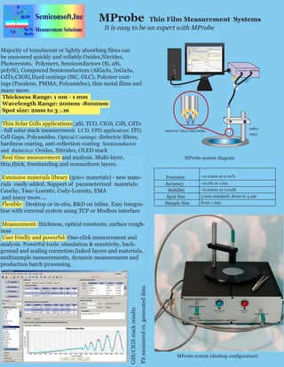
- 1. LIGHT SOURCESPECTROMETER LIGHT - INLIGHT-OUT FIBEROPTICS REFLECTANCE PROBESAMPLE STANDUSB 2 CABLE MProbe system diagram MProbe system (desktop configuration) Precision <0.01nm or 0.01% Accuracy <0.2% or 1 nm Stability <0.02nm or 0.03% Spot Size 3 mm standard, down to 3 mm Sample Size from 1 mm Majority of translucent or lightly absorbing films can be measured quickly and reliably:Oxides,Nitrides, Photoresists, Polymers, Semiconductors (Si, aSi, polySi), Compound Semiconductors (AlGaAs, InGaAs, CdTe,CIGS),Hard coatings (SiC, DLC), Polymer coatings (Paralene, PMMA, Polyamides), thin metal films and many more. Thickness Range: 1 nm - 1 mm Wavelength Range: 200nm -8000nm Spot size: 2mm to 3 mm Thin Solar Cells applications: aSi, TCO, CIGS, CdS, CdTe - full solar stack measurement. LCD, FPD application: ITO, Cell Gaps, Polyamides. Optical Coatings: dielectric filters, hardness coating, anti-reflection coating Semiconductor and dielectics: Oxides, Nitrides, OLED stack Real time measurement and analysis. Multi-layer, thin,thick, freestanding and nonuniform layers. Extensive materials library (500+ materials) - new materials easily added. Support of parameterized materials: Cauchy, Tauc-Lorentz, Cody-Lorentz, EMA and many more.... Flexible: Desktop or in-situ, R&D on inline. Easy integration with external system using TCP or Modbus interface Measurement: thickness, optical constants, surface roughness User friedly and powerful: One-click measurement and analysis. Powerful tools: simulation & sensitivity, background and scaling correction,linked layers and materials, multisample measurements, dynamic measurement and production batch processing. MProbe Thin Film Measurement Systems It is easy to be an expert with MProbe CdS/CIGS stack results Fit measured vs. generated data
- 2. Basic Specification Model Wavelength range Spectrometer/Detector/Light source Thickness range* VIS 400-1100 nm Spectrometer F4/Si 3600 pixels/ Tungsten - Halogen light source 15 nm to 20 mm (option:up to 50 mm) UVVisSR 200-1000 nm Spectrometer F4/ Si CCD 3600 pixels/ Deuterium & Tungsten-Hal-ogen light source 1 nm to 20 mm (option:up to 50 mm) HRVIS 700-1000 nm HR Spectrometer F4/Si 3600 pix-els/ Tungsten - Halogen light source 1 mm to 400 mm NIR 900-1700nm Transmission Spectrometer (TVG) F2/512 InGaAs/Tungsten-Halogen light source 100 nm-200 mm VISNIR 400-1700 nm Spectrometer F4 Si CCD 3600 pixels(Vis channel);Transmission Spectrometer (TVG)F2/512 InGaAs PDA( NIR channel) Tungsten-Halogen light source 15 nm to 200 mm UVVIS-NIR 200 -1700 nm Spectrometer F4 Si CCD 3600 pixels(Vis channel);Transmission (TVG) F2/512 InGaA ( NIR channel) Deuterium & Tungsten-Halogen light source 1 nm -300 mm NIRScan 2000nm -6000nm (option: up to 8000nm) FTIR spectrometer with MCT detec-tor (scan time from 4 sec ), low CCT light source 100 nm -800 mm XT 1590nm -1650nm Transmission Spectrometer (TVG) F2/512 InGaAs/Tungsten-Halogen light source 10 mm- 1 mm * T, n & k measurement in 25nm - 5mm thickness range Other configuration are available. OEM inquiries and custom development projects are welcome. One year limited warranty on labor and materials for all system. Semiconsoft, Inc, 2012 tel. +1.617.388.6832 email: info@semiconsoft.com fax.+1.508.858.5473 Visit us : http://www.semconsoft.com 1nm 10nm 100nm 1mm 100mm 1mm XT NIRScan UVVISNIR VISNIR NIR HRVIS USVISSR 10mm