
Recommandé
Contenu connexe
Tendances
Tendances (20)
En vedette
En vedette (15)
Similaire à 107 yun-yu wang - 7538029 - method of room temperature growth of si ox on silicide as an etch stop layer for metal contact open of semiconductor devices
Similaire à 107 yun-yu wang - 7538029 - method of room temperature growth of si ox on silicide as an etch stop layer for metal contact open of semiconductor devices (20)
Plus de Mello_Patent_Registry
Plus de Mello_Patent_Registry (20)
Dernier
Dernier (20)
107 yun-yu wang - 7538029 - method of room temperature growth of si ox on silicide as an etch stop layer for metal contact open of semiconductor devices
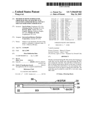
- 1. c12) United States Patent Wang et al. (54) METHOD OF ROOM TEMPERATURE GROWTH OF SIOx ON SILICIDE AS AN ETCH STOP LAYER FOR METAL CONTACT OPEN OF SEMICONDUCTOR DEVICES (75) Inventors: Yun-Yu Wang, Poughquag, NY (US); Christian Lavoie, Ossining, NY (US); Kevin E. Mello, Fishkill, NY (US); Conal E. Murray, Yorktown Heights, NY (US); Matthew W. Oonk, Poughkeepsie, NY (US) (73) Assignee: International Business Machines Corporation, Armonk, NY (US) ( *) Notice: Subject to any disclaimer, the term ofthis patent is extended or adjusted under 35 U.S.C. 154(b) by 288 days. (21) Appl. No.: 11/160,699 (22) Filed: Jul. 6, 2005 (65) Prior Publication Data US 2007/0010093 Al Jan. 11, 2007 (51) Int. Cl. HOJL 21144 (2006.01) (52) U.S. Cl. ....................... 438/655; 438/675; 438/637; 257/E21.593 (58) Field of Classification Search .................. 438/655 See application file for complete search history. (56) References Cited U.S. PATENT DOCUMENTS 5,912,188 A * 6/1999 Gardner et al............... 438/740 BOX 111111 1111111111111111111111111111111111111111111111111111111111111 US007538029B2 (10) Patent No.: US 7,538,029 B2 May 26,2009(45) Date of Patent: 5,913,139 A * 6,114,734 A * 6,144,097 A * 6,211,083 B1 * 6,287,951 B1 * 6,436,841 B1 * 6,500,728 B1 * 6,551,901 B1 * 2001/0019898 A1 * 2002/0068429 A1 * 2004/0067635 A1 * 2004/0070036 A1 * 2005/0064721 A1 * 2005/0110070 A1 * 2005/0158986 A1 * 2006/0057844 A1 * 6/1999 Hashimoto et al........... 438/618 9/2000 Eklund ....................... 257/410 1112000 Asahina et al.............. 257/751 4/2001 Yang eta!. .................. 438/682 9/2001 Lucas eta!. ................. 438/618 8/2002 Tsai eta!. ................... 438/738 12/2002 Wang ......................... 438/424 4/2003 Gu eta!. ..................... 438/424 9/2001 Arafa eta!. ................. 438/740 6/2002 Trivedi ....................... 438/618 4/2004 Wu et a!. .................... 438/624 4/2004 Setton ........................ 257/410 3/2005 Tsai eta!. ................... 438/740 5/2005 Omura ....................... 257/311 7/2005 Wu eta!. .................... 438/634 3/2006 Domenicucci et a!. ...... 438/655 FOREIGN PATENT DOCUMENTS JP 2000216383 A * 8/2000 * cited by examiner Primary Examiner-Marcos D. Pizarro Assistant Examiner-Igwe U. Anya (74) Attorney, Agent, or Firm-Yuamnin Cai; Howard Cohn (57) ABSTRACT Silicide is protected during MC RIE etch by first forming an oxide film over the silicide and, after performing MC RIE etch, etching the oxide film. The oxide film is formed from a film of alloyed metal-silicon (M-Si) on the layer of silicide, then wet etching the metal-silicon. An ozone plasma treat- ment process can be an option to densify the oxide film. The oxide film may be etched by oxide RIE or wet etch, using 500:1 DHF. 13 Claims, 2 Drawing Sheets SILICON 204
- 2. U.S. Patent May 26,2009 Sheet 1 of2 US 7,538,029 B2 100 /107 ; (SILICIDE ..~!~... :~----------------t~1~: 102 BOX "-SILICON 101 Si-SUBSTRATE FIG. 1A (PRIORART) 100 ; 112 c DIELECTRIC (NITRIDE STI I L-- I......... 102 BOX '-SILICON 101 Si-SUBSTRATE FIG. 1B (PRIOR ART) BOX SILICON FIG. 2A 2001 / Si02 STI I I '......... "-SILICON "-SILICIDE202 BOX FIG. 28 v1 v1 f-- ~ 10 08 106 104 204 222 206v 1'- 204
- 3. U.S. Patent [SiN I I I 202 FIG. 2C rSiN I I I 202 FIG. 2D FIG. 3 May 26,2009 Sheet 2 of2 US 7,538,029 B2 212 DIELCTRIC (SiN l I BOX '-OXIDE .._SILICON "SILICIDE 212' DIELCTRIC /SiN l I I BOX .. Si02 .._SILICON "siLICIDE 315 300~ r· ( y316 314 3111 - r313 1-r (~/ STI L310 317 318 '--312 STI 304- 302 BOX- 301 Si-SUBSTRATE- ' 210 __j 3~8 v-222 206f-._/"" ~'--204 ~0 3~8 /222 206 04-----·'--2
- 4. US 7,538,029 B2 1 METHOD OF ROOM TEMPERATURE GROWTH OF SIOx ON SILICIDE AS AN ETCH STOP LAYER FOR METAL CONTACT OPEN OF SEMICONDUCTOR DEVICES BACKGROUND OF THE INVENTION 2 ness ofabout 200-300 Angstroms, and is suitably formed by traditional salicidation process (deposit metal, heat, etch, heat again). An area 107 disposed on the side oflayer 104 and 106 is shallow trench isolation (STI). A layer 108 of nitride is used to cap the silicide layer 106. The nitride layer 108 typically has a thickness of about 500 Angstroms, and is suitably formed by Chemical Vapor Depo- sition (CVD). Silicon Nitride (Si3N4 ; often referred to simply The invention relates to semiconductor device fabrication teclmiques and, more particularly, to teclmiques for etching through a dielectric layer to an underlying silicide layer. 10 as "nitride"; often abbreviated as "SiN") is a dielectric mate- rial which is commonly used to provide an excellent mask (barrier) against oxidation of silicide during the subsequent dielectric deposition 110 such as SiOx deposition at high temperature. Typically, source and drain regions in a modern MOSFET (Metal-Oxide-Semiconductor Field-Effect-Transistor) devices are formed with overlying silicide as the contact. Silicides are alloys of silicon and metals, and are used as contact materials in silicon device manufacturing. Exemplary 15 silicides are cobalt silicide (CoSi2), nickel Silicide (NiSi), titanium silicide (TiSi2), tungsten silicide (WSi2 ), tantalum silicide (TaSi2), and platinum silicide (PtSi). Silicides are commonly used as conductors and contact materials in silicon semiconductor teclmology due to their 20 high conductivity, compatibility with silicon, and suitability to small-geometry semiconductor devices. The high conduc- tivity (low resistivity) of source/drain silicide serves to mini- mize the contribution of parasitic resistance in the source drain region to the series resistance ofMOSFET devices that 25 employ it. The parasitic series resistance of silicide itself is often so small that its contribution to total series resistance is considered to be negligible and not a limiting factor to device performance. In the MC (Metal Contact) RIE (Reactive Ion Etching) 30 process, due to poor selectivity of nitride RIE and silicide, MC RIE is normally etched into silicide. In 90 urn teclmology for silicon on insulator (SOl), because of thin Si, sometimes the MC RIE punches through the silicide and touches the surface of Si which causes weak driving current problems or 35 contact resistance problems. It is well known that Si02 can be used to act as a good RIE stop for the nitride RIE. Normally, silicide is covered with nitride which has a poor selectivity between nitride RIE and silicide. In order to protect the silicide from nitride etch, a thin 40 oxide layer between silicide and nitride as an etch stop is preferred. However, conventional SiOx deposition can cause the oxidation ofsilicide and it creates a resistance problem. In order to avoid the oxidation of silicide, a thin oxide layer on top of silicide is preferably applied at room temperature. 45 Reactive Ion Etching (RIE) is a variation ofplasma etching in which, during etching, a semiconductor wafer is placed on A layer 110 ofdielectric material is formed over the nitride layer 108. The dielectric layer 110 typically has a thickness of about 5000 Angstroms, and is suitably formed by CVD. Then, MC (Metal Contact) RIE is performed to open a via (contact hole) 112, through the layers 110 and 108, to the underlying silicide 106. (MC RIE in general refers to both the dielectric and nitride etch (one process). (The RIE chemistry changes during the contact etch.) The resulting structure is shown in FIG. lB. Finally, a thin layer (liner) ofTi/TiN (titanium nitride), not shown, is deposited in the contact hole 112, which is ulti- mately filled with a conductor such as tungsten (W). As best viewed in FIG. lB, during MC RIE, the underlying silicide layer 106 is compromised (thinned, etched). This becomes a problem when the silicide 106 is thin and the Ti/TiN liner would then land on top ofthe silicon 104 instead ofon the silicide 106, and this can cause a contact resistance problem. In the extreme case, MC RIE with sputter clean can cause the bottom of the MC to penetrate into the silicon and touch the bottom ofSi (or top of buried oxide surface). A solution to this problem is simply to ensure that the silicide layer 106 is thick enough to withstand some etching during MC RIE. However, the downside of such an approach would be Si consummption and contact resistance problems. In bulk (non SOl) teclmology, the problem would bejunction leakage. SUMMARY OF THE INVENTION It is an object of the invention to provide an improved teclmique for fabricating semiconductor devices having sili- cide contact areas under contact holes through dielectric. a RF (radio frequency) poweredelectrode. The wafertakes on a potential which accelerates etching species extracted from the plasma toward the etched surface. The chemical etching reaction is preferentially taking place in the direction normal to the surface, i.e. etching is more anisotropic than in plasma etching but is less selective. Although RIE leaves the etched surface damaged, it is a very common etching mode in semi- conductor manufacturing. According to the present invention, a chemical etching 50 method is used to grow a thin layer ofSi02 as an etch stop on top of silicide. FIGS.lA and lB illustrate a process 100 ofthe prior art, for etching through a dielectric layer to an underlying silicide layer of a semiconductor device. According to the invention, a room temperature oxide film is formed under the nitride cap and functions as an RIE selective layer etch stop. Room temperature oxide formation 55 is suitably performedby an alloyed metal Si (M-Si) sputtering process with subsequent wet etch to remove metal and oxide the residual Si, thus forming a thin layer of SiOx on top of silicide as well as on top of STI region. A layer 104 of single crystalline silicon is bonded on a semiconductor (single crystal silicon) substrate (wafer) 101 60 through buried oxide 102 (BOX). The layer 104 typically has Silicon dioxide (Si02 , often referred to simply as "oxide") is a common insulator in semiconductor device teclmology, particularly in silicon MOS/CMOS (Metal-Oxide-Semicon- ductor/Complementary MOS) where it is use as a gate oxide. High quality films may be obtained by thermal oxidation of silicon. Typically, in the composition of the M-Si, the Si is a thickness of 500-700 Angstroms. This is a typical vendor- supplied SOl (Silicon On Insulator) wafer. The silicon sub- strate 101 is shown much thinner than in reality (i.e., not to scale), for illustrative clarity. A layer 106 ofsilicide is formed atop the layer 104 ofsingle crystalline silicon. The silicide layer 106 typically has a thick- 65 about 10%-30% by atomic number, preferably about 15%- 25% by atomic number and most preferably about 20% by atomic number (or atomic percentage).
- 5. US 7,538,029 B2 3 The present invention, providing an oxide film over the silicide, benefits from the fact that MC nitride RIE is more selective to oxide than silicide, therefore protecting the sili- cide. 4 DETAILED DESCRIPTION OF THE INVENTION In the description that follows, numerous details are set forth in order to provide a thorough understanding of the present invention. It will be appreciated by those skilled in the art that variations of these specific details are possible while still achieving the results of the present invention. Well- known processing steps are generally not described in detail in order to avoid unnecessarily obfuscating the description of According to the invention, a method of forming a semi- conductor device having a layer of silicide and a contact opening extending through an overlying dielectric layerto the layer ofsilicide is disclosed. The method comprises the steps of: before etching the contact opening, forming an room temperature oxide film over the layer of silicide without oxi- dizing silicide; and after etching the contact opening, etching the oxide film to expose the underlying silicide. 10 the present invention. Materials (e.g., silicon dioxide) may be referred to by their formal and/or common names, as well as by their chemical formula. Regarding chemical formulas, numbers may be pre- sented in normal font rather than as subscripts. For example, silicon dioxide may be referred to simply as "oxide", chemi- The step ofetching the oxide film may comprise perform- ing oxide reactive ion etching (RIE) or using 500:1 DHF. The step of forming the oxide film may comprise: first forming a film ofalloyed metal-silicon (M-Si) on the layer of silicide; and then forming the oxide film by wet etching the metal-silicon. The metal M in the alloyed metal-silicon (M-Si) is selected from the group consisting ofTi, Ni, Co, or other transition metal. 15 cal formula Si02 . For example, silicon nitride (stoichiometri- cally Si3N4 , often abbreviated as "SiN") may be referred to simply as "nitride". In the description that follows, exemplary dimensions may be presented for an illustrative embodiment ofthe invention. An ozone plasma treatment process may be performed to densify the oxide. 20 The dimensions should not be interpreted as limiting. They are included to provide a sense of proportion. Generally speaking, it is the relationship between various elements, where they are located, their contrasting compositions, and According to the invention, a method ofprotecting silicide during MC RIE etch comprises: before performing MC RIE 25 etch, forming an oxide film over the silicide; and after per- forming the MC nitride RlE etch stopping on top ofthin oxide film, etching the oxide film. The oxide film may be RIE etched or wet etched. According to the invention, a semiconductor device com- 30 prises: a layer ofsilicide; a layerofoxide overthe silicide; and sometimes their relative sizes that is of significance. Inthe drawings accompanying the description that follows, often both reference numerals and legends (labels, text descriptions) will be used to identifY elements. Iflegends are provided, they are intended merely as an aid to the reader, and should not in any way be interpreted as limiting. The invention relates to semiconductor device fabrication techniques and, more particularly, to techniques involving etching through a dielectric layer to an underlying silicide layer. a layer ofnitride over the layer ofoxide. The device may be a FET having source and drain regions and a gate electrode, and the layer of silicide is over the source and drain regions and the gate electrode. As discussed hereinabove, silicide and underlying silicon 35 can be compromised during MC RIE. FIGS. 2A-2D illustrate an exemplary embodiment 200 of the invention. An exemplary starting structure comprises a substrate (not shown, compare 101) with a layer 202 (com- pare 102) of buried oxide (BOX) and a layer 204 (compare 104) of silicon bonded on the BOX, with an overlying layer The invention can be applied generally to thin film process- ing for the fabrication of structures for microelectronics or other nanotechnologies. The invention can be applied to any fabrication process where silicon dioxide is required above a metal silicide (and a contact hole must be made, such as by MC RlE, through the oxide). 40 206 (compare 106) of silicide formed atop the layer 204 of silicon, and shallow trench isolation (STI, compare 107). This is conventional and is known. BRIEF DESCRIPTION OF THE DRAWINGS In a first step of the process, a film 220 of alloyed metal silicon (M-Si) is blanket deposited (formed) on top of the 45 silicide 206 and the STI 107 by a sputtering process (physical vapor deposition). The film 220 typically has a thickness of approximately 50-100 Angstrom, and is suitably formed by sputter deposition process. The resulting structure is shown in FIG. 2A The structure, operation, and advantages of the present invention will become further apparent upon consideration of the following description taken in conjunction with the accompanying figures (FIGS.). The figures are intended to be illustrative, not limiting. Certain elements in some of the 50 figures may be omitted, or illustrated not-to-scale, for illus- trative clarity. The cross-sectional views may be inthe form of "slices", or "near-sighted" cross-sectional views, omitting certain background lines which would otherwise be visible in a "true" cross-sectional view, for illustrative clarity. 55 FIG. 1A is a cross-sectional view illustrating an initial step in an exemplary process for performing MC RIE, according to the prior art. FIG. 1B is a cross-sectional view illustrating a further step 60 in the process of the prior art; FIGS. 2A-2D are cross-sectional views illustrating an embodiment ofa process for performing MC RIE, according to the invention; and FIG. 3 is a simplified cross-sectional view of a semicon- 65 ductor device which has been formed utilizing the process of the invention. In a next step ofthe process, metal in the M-Si film 220 is chemically etched away and the residual Si is oxidized, form- ing a SiOx on top of silicide. The resulting oxide film 222 (FIG. 2B) is a thin, protective layer, approximately 20-50 Angstroms thick. By doing this, Si02 that is formed on top ofthe silicide 206 can be used as an etch stop for subsequent nitride opening. The metal Si can be CoxS~, TixSiY, or NixSiy- Normally, the etch solution is H2 S04 with H2 0 2 . H2 0 2 oxidizes both metal and Si. H2 S04 dissolves metal oxide and leaves Si02 on the surface of the silicide as in the following chemical reaction. The following is the chemical reaction sequence: where M can be Ti, Ni, Co, or other transition metal.
- 6. US 7,538,029 B2 5 Since the transition metals are the 38 elements in groups 3 through 12 of the periodic table whose valence electrons are present in more than one shell, they often exhibit several oxidation states. The reason that this method works is that metal is dissolved 5 away in the solution, while residual Si does not dissolve in the solution, but instead is oxidized by the solution. At the same time, the solution itself does not attack either the SiOx and silicide in the structure. A critical aspect ofthis method is that metal and Si have to be evenly intermixed in the thin film on 10 top ofthe structure and the majority ofthe element in the film has to be metal in order for it to work. Ifthe majority of the element in the film is Si, the reaction would be self-limiting, which means that only the top surface ofthe film is oxidized, forming SiOx film. The bottom part of the film would be protected by the top SiOx film from further wet etching from 15 the solution. Thus it would create a conductive film across silicide and STI causing a metal short. Ifthe Si concentration is too low, such as less than 5% (atomic percent), in order to grow an equivalent film thickness, it requires thicker M-Si deposition, which is not practical. Therefore, the concentra- 20 tion of Si in the metal-Si target is important to make the method work. Typically, in the composition of the M-Si, the 6 silicide 311, 313, 315 atop the source and drain junctions and the gate electrode, respectively; and shallow trench isolation (STI) on both sides of the FET. Oxide and nitride (omitted, for illustrative clarity) are formed as described hereinabove. Overlying silicon dioxide is formed and MC etched, as described hereinabove (omitted, for illustrative clarity). Although the invention has been shown and described with respect to a certain preferred embodiment or embodiments, certain equivalent alterations and modifications will occur to others skilled in the art upon the reading and understanding of this specification and the annexed drawings. In particular regard to the various functions performed by the above described components (assemblies, devices, circuits, etc.) the terms (including a reference to a "means") used to describe such components are intended to correspond, nnless other- wise indicated, to any component which performs the speci- fied function of the described component (i.e., that is func- tionally equivalent), even though not structurally equivalent to the disclosed structure which performs the function in the herein illustrated exemplary embodiments ofthe invention. In addition, while a particular feature ofthe invention may have been disclosed with respect to only one of several embodi- ments, such feature may be combined with one or more features of the other embodiments as may be desired and Si is about 10%-30% by atomic weight, preferably about 15%-25% by atomic weight and most preferably about 20% by atomic weight. 25 advantageous for any given or particular application. What is claimed is:An ozone plasma treatment can be used as an option to densify the oxide 222. The resulting structure is shown in FIG. 2B. In a next step ofthe process, in a manner comparable to the the steps described hereinabove with respect to FIGS. 1A and 1B; i.e., a nitride capping layer 208 (compare 108) is depos- ited (on top ofthe SiOx films); dielectric 210 (compare 110) 1. A method of forming a semiconductor device having a layer of silicide and a contact opening extending through an overlying dielectric layer to the layer of silicide, the method 30 comprising the steps of: is deposited; and MC RIE is performed (opening a hole in the dielectric and the nitride). When the nitride layer 208 is opened, MC RIE stops on top of the oxide film 222. (compare contact opening 212 with 35 opening 112). The resulting structure is shown in FIG. 2C. The nitride layer (208), also called "barrier nitride", serves as a a diffusion barrier to protect the device from contamina- tion (ionics from the BEOL (back end ofline)). In a final step of the process, oxide RIE is performed to 40 open the oxide 222, down to the silicide 206. The resulting structure is shown in FIG. 2D. (Contact opening is now labeled 212'.) before etching the contact opening, forming an oxide film over the layer of silicide; and after etching the contact opening, etching the oxide film to expose the underlying layer of silicide; and wherein the step of forming the oxide film comprises: first forming a film of alloyed metal-silicon (M-Si) on top of the layer of silicide; and then forming the oxide film by wet etching the metal- silicon to remove the metal and to oxidize the residual Si to form a layer of SiOx on top of the silicide. 2. The method of claim 1, wherein the step of etching the oxide film comprises: performing oxide reactive ion etching (RIE). 3. The method of claim 1, wherein the step of etching theAlternatively, a wet etch of500: 1 DHF can be used to open Si02, and this may be preferred over the RIE open. 45 oxide film comprises: using 500:1 DHF.Hydrofluoric acid (HF) is a very hazardous acid commonly used in silicon processing to etch silicon dioxide, Si02 . It is also an important component ofessentially all surface clean- ing recipes. Dilute HF (DHF) is dilute HF. A Si02 etching solution may comprise 49% HF in water (H2 0). A typical 50 mixture would be 1 part HF: 100 parts H20. In an exemplary application for the invention, the device is an FET (field effect transistor), and the silicide forms contact over the source (S), gate (G) and drain (D) regions ofthe FET. FIG. 3 is a simplified cross-sectional diagram ofa FET 300 of the prior art, formed using the techniques of the present 55 invention. The FET 300 is suitably one half of a CMOS (complementary metal oxide semiconductor) pair of PETs. The FET 300 is formed in a silicon layer 304 (compare 204) on a layer of BOX 302 (compare 202) on a silicon substrate 301 (compare 101), and, as is known, generally comprises: a first source (or drain) junction 310; a second drain (or source) junction 312; a first extension implant 317; a first extension implant 318; 60 a gate electrode 314 between the source and drain june- 65 tions; sidewall spacers 316 on both sides of the gate structure; 4. The method of claim 1, further comprising the step of: before applying the dielectric layer, depositing a nitride capping layer. 5. The method of claim 1, wherein: the metal in the alloyed metal-silicon (M-Si) is selected from the group consisting ofwhere M can be Ti, Ni, Co, or other transition metal. 6. The method of claim 1, wherein: the wet etching comprises an etch solution of H2 S04 with H202. 7. The method of claim 1, further comprising the step of: performing an ozone plasma treatment to densifY the oxide. 8. The method of claim 1, wherein the device is a field effect transistor (FET), and the silicide comprises source and drain regions of the FET. 9. A method of protecting silicide during MC RIE etch comprising: before performing MC RIE etch, forming an oxide film over the silicide; and wherein the step of forming the oxide film comprises:
- 7. US 7,538,029 B2 7 first forming a film of alloyed metal-silicon (M-Si) on the layer of silicide; and then, forming the oxide film by wet etching the metal- siliconto remove the metal M and to oxidize the residual Si to form a layer of SiOx on top ofthe silicide; and forming a nitride layer over the oxide film. 10. The method of claim 9, further comprising: performing an ozone plasma treatment to densifY the oxide. 8 11. The method ofclaim 9, further comprising: after performing MC RIE etch, etching the oxide film. 12. The method ofclaim 11, wherein the step ofetching the oxide film comprises: performing oxide reactive ion etching (RIE). 13. The method ofclaim 11, wherein the step ofetching the oxide film comprises: a wet etch using 500:1 DHF. * * * * *