1. MicrClap Switch Circuit for Devices
January 11, 2014 By Administrator Leave a Comment
We have already seen the circuit diagram, working and applications of 9 way Clap Switch Circuit. Now, we
are going to deal another circuit named clap switch circuit for devices. Summary is given below:
Summary of Clap switch Circuit:
If you wish to “ON” and “OFF” the device without a penny shifting from your space then this circuit is
helpful for you.
One more plus point of this circuit is that there is no fear of the electrical shocks as you are not required to
touch any of the mechanical switches physically.
Visual indication of the devices is also provided to you.
With the help of this circuit, speed of the fan can also be controlled by connecting regulator with individual
outputs.
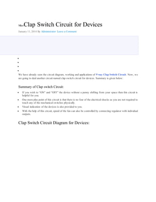
Clap Switch Circuit Diagram for Devices:
2. Circuit Diagram of Clap Switch – ElectronicsHub.Org
Description:
Along with some of the other components, this circuit is mainly based on the two ICs i.e. NE555 timer along
with CD4017.
IC 555 timer in this circuit is wired like a monostable oscillator. For this circuit, IC NE555 monostable
produces a clock pulse, which is used to give an oscillating wave at IC1 pin 3 which is an output pin.
Monostable (or you can say one shot multivibrator) contains only one steady state and all we need is to trigger
it externally to return it in reverse direction to its original state.
Another one is the CD4017 which is a CMOS counter/divider IC. It receives a clock signal through the clock
input and in the sequential manner it turns ON all the 10 outputs, every time it gets the clock input pulse.
In order to get familiar with the working of the IC, it is essential for the one to get familiar with the every pin
of the IC. These IC consist of 3 input pins along with 10 output pins also have one pin for ground and one
more for the power supply and one more pin for the Carry out. Pin diagram of the IC is designed below -
3. 1. Input Pin:
1. Reset Pin (Pin 15) – The counter is reset to the zero position by this pin. Suppose you wish that
the counter will only count till third position then you need linked the fourth pin with 15 pin. So
after reaching to the third output it will automatically begin its counting from zero.
2. Clock Pin (Pin14) – In each of the timing pin 14 moves at high the output will be given to you.
From the initial clock pulse output will be received at the pin 3 likewise for the next clock pulse
output will be received at the pin 2 and so on.
3. Clock Inhibit Pin (Pin 13) – The counter is switched to “on” and “off” by this pin. If you need
that the counter to be switched off then for that pin 13 must be at high state. If the pin is at high
then it will disregard the clock pulse without paying attention that how much time you press the
switch i.e. the count will not go forward. Pin 13 in our circuit is grounded.
2. Output Pin (Pin Q0- Q9) -It is used to get the input in chronological order. Like pin 3 will give you the
output for the first pulse and so on.
3. Ground Pin (Pin 8) and Supply pin (pin 16) – For the proper working of these IC these pins are used
to give ground as well as power supply.
4. Carry out Pin (Pin 12) – These pins are used to link one or more CD4017 IC with each other.
Suppose you have a desire to connect one more CD4017 IC then attach pin 12 to the clock input to its
next one. The carry pin of first CD4017 is connected to clock input of the second and the carry pin of the
second is connected to the clock input of the third and so on. In our circuit we left this pin as we have
desire of only one IC in our circuit.
Working of Clap Switch Circuit:
At the time when some one slap in front of the Mic the sound signal is converted into the electrical signal by
the condenser microphone.These signals are then given to the transistor T1 base which in return trigger the IC1
pin2. And with the help of the formula shown below the time period for which the output stay in the high
position can be calculated -
T = 1.1*R5*C4
4. At the moment the output from the IC1 pin 3 is given to CD4017 decade counter 14 pin, which supply a clock
pulse for the proper working of IC2. The counting of the CD4017 begins from the zero after getting the clock
input. And it moves to forward one by one at each time whenever pin 14 moves to high (as in front of the mic
we clap). Like we get output from the pin 2 for the first clap i.e. Q1 and LED1 will shine and the device
connected to relay start operating . While for the second clap output will receive at pin 4 and LED2 will shine
while at this time LED1 turn off and so on. At each output point you need to attach the individual relay .10
individual devices can be controlled with the help of this circuit just connect the relay at appropiate outputs of
CD4017.
Components used in this Circuit:
IC
o IC1(NE555) – 1
o IC2(CD4017) – 1
Resistor
o R1,R4(10K) – 2
o R2,R7,R8,R9(1K) – 4
o R3(2.2K) – 1
o R5(220E) – 1
o R6(150) – 1
C1,C2(.1uf) – 2
C3(1uf) – 1
C4(4.7uf) – 1
Mic – 1
LED – 3
T1(BC548) – 1
T2,T3,T4(BC547) – 3
Relay – 3
Note: For some more interesting projects and circuit diagrams, visit Mini Projects on Electronics