M3488 datasheet
•
1 j'aime•400 vues

Datasheet related to 256X256 PCM channel SWITCH invented by Piero Belforte (CSELT LABS) in 1979 as ECI (Elemento di Commutazione Integrato). The ECI serves about 27 Million public telephone lines worldwide

Recommandé
Contenu connexe
Tendances
Tendances (20)
En vedette
En vedette (20)
Similaire à M3488 datasheet
Similaire à M3488 datasheet (20)
Plus de Piero Belforte
Plus de Piero Belforte (20)
Dernier
Dernier (20)
M3488 datasheet
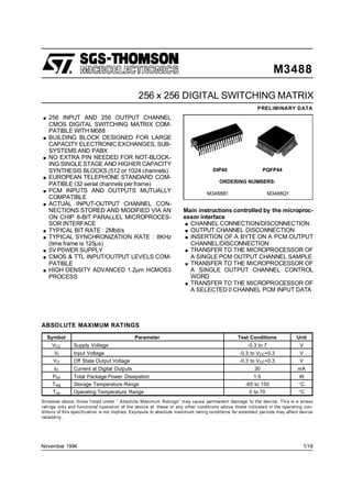
- 1. M3488 November 1994 256 x 256 DIGITAL SWITCHING MATRIX PRELIMINARY DATA This is advanced information on a new product now in development or undergoing evaluation. Details are subject to change without notice. .256 INPUT AND 256 OUTPUT CHANNEL CMOS DIGITAL SWITCHING MATRIX COM- PATIBLE WITH M088 .BUILDING BLOCK DESIGNED FOR LARGE CAPACITY ELECTRONIC EXCHANGES, SUB- SYSTEMS AND PABX .NO EXTRA PIN NEEDED FOR NOT-BLOCK- ING SINGLE STAGE AND HIGHER CAPACITY SYNTHESIS BLOCKS (512 or 1024 channels) .EUROPEAN TELEPHONE STANDARD COM- PATIBLE (32 serial channels per frame) .PCM INPUTS AND OUTPUTS MUTUALLY COMPATIBLE .ACTUAL INPUT-OUTPUT CHANNEL CON- NECTIONS STORED AND MODIFIED VIA AN ON CHIP 8-BIT PARALLEL MICROPROCES- SOR INTERFACE .TYPICAL BIT RATE : 2Mbit/s .TYPICAL SYNCHRONIZATION RATE : 8KHz (time frame is 125µs) .5V P0WER SUPPLY .CMOS & TTL INPUT/OUTPUT LEVELS COM- PATIBLE .HIGH DENSITY ADVANCED 1.2µm HCMOS3 PROCESS Main instructions controlled by the microproc- essor interface .CHANNEL CONNECTION/DISCONNECTION .OUTPUT CHANNEL DISCONNECTION .INSERTION OF A BYTE ON A PCM OUTPUT CHANNEL/DISCONNECTION .TRANSFER TO THE MICROPROCESSOR OF A SINGLE PCM OUTPUT CHANNEL SAMPLE .TRANSFER TO THE MICROPROCESSOR OF A SINGLE OUTPUT CHANNEL CONTROL WORD .TRANSFER TO THE MICROPROCESSOR OF A SELECTED 0 CHANNEL PCM INPUT DATA DIP40 PQFP44 ORDERING NUMBERS: M3488B1 M3488Q1 ABSOLUTE MAXIMUM RATINGS Symbol Parameter Test Conditions Unit VCC Supply Voltage -0.3 to 7 V VI Input Voltage -0.3 to VCC+0.3 V VO Off State Output Voltage -0.3 to VCC+0.3 V IO Current at Digital Outputs 30 mA Ptot Total Package Power Dissipation 1.5 W Tstg Storage Temperature Range -65 to 150 °C Top Operating Temperature Range 0 to 70 °C Stresses above those listed under ” Absolute Maximum Ratings” may cause permanent damage to the device. This is a stress ratings only and functional operation of the device at these or any other conditions above those indicated in the operating con- ditions of this specification is not implied. Exposure to absolute maximum rating conditions for extended periods may affect device reliability. 1/18
- 2. PQFP44 PIN CONNECTIONS (Top views) DIP40 EXCHANGE NETWORKS APPLICATIONS 256 PCM links network (160 or 192 DSM) : the 32 x 32 link module shown on the next page. 2048 PCM links network (1792 or 2048 DSM) : the 256 x 256 link network is shown above. 1 2 3 5 6 4 7 8 9 10 17 11 18 19 20 21 22 44 43 42 41 3940 38 37 36 35 34 28 27 26 24 23 25 33 32 31 29 30 SYNC CLOCK INP PCM7 VCC INP PCM0 N.C. D7 D6 D5 N.C. D4 D3 D2 D1 D0 DR N.C. OUTPCM7 RD VSS C/D A1 A2 S2 S1 N.C. WR CS1 RESET CS2 D93TL040A 12 13 14 15 16 INP PCM6 INP PCM5 INP PCM4 INP PCM3 INP PCM2 INP PCM1 OUTPCM6 OUTPCM5 OUTPCM4 N.C. OUTPCM3 OUTPCM2 OUTPCM1 OUTPCM0 M3488 2/18
- 3. EXCHANGE NETWORKS APPLICATIONS (continued) Single Stage/Sixteen Devices Configuration (32 by 32 links or 1024 channels). M3488 3/18
- 5. RECOMMENDED OPERATING CONDITIONS Symbol Parameter Value Unit VCC Supply Voltage 4.75 to 5.25 V Vi Input Voltage 0 to 5.25 V VO Off State Input Voltage 0 to 5.25 V CLOCK Freq. Input Clock Frequency 4.096 MHz SYNC Freq. Input Synchronization Frequency 8 KHz Top Operating Temperature 0 to 70 °C CAPACITANCES (measurement freq. = 1MHz; Top = 0 to 70°C; unused pins tied to VSS) Symbol Parameter Pins (*) Min. Typ. Max. Unit CI Input Capacitance 6 to 15; 26 to 30; 32 to 36 5 pF CI/O I/O Capacitance 20 to 24 15 pF CO Output Capacitance 1 to 4; 17 to 19; 25; 37 to 40 10 pF D.C. ELECTRICAL CHARACTERISTICS (Tamb = 0 to 70°C, VCC = 5V ±5%) All D.C. characteristics are valid 250µs after VCC and clock have been applied. Symbol Parameter Pins (*) Test Condition Min. Typ. Max. Unit VILC Clock Input Low Level 6 -0.3 0.8 V VIHC Clock Input High Level 6 2.4 VCC V VIL Input Low Level 7 to 15 20 to 24 26 to 30 32 to 36 -0.3 0.8 V VIH Input High Level 7 to 15 20 to 24 26 to 30 32 to 36 2 VCC V VOH Output High Voltage (Level) 17 to 25 IOH = 5mA 2.4 V IOH Output High Current VOH = 2.4V 5 mA VOL Output Low Voltage (Level) 1 to 4 37 to 40 17 to 25 IOL = 5mA 0.4 V IOL Output Low Current VOL = 0.4V 5 mA IIL Input Leakage Current 6 to 15 26 to 30 32 to 36 VIN = 0 to VCC 5 µA IDL Data Bus Leakage Current 17 to 24 VIN = 0 to VCC VCC applied; Pins 35 and 36 tied to VCC, after Device Initialization ±5 µA ICC Supply Current 16 Clock Freq. = 4.096MHz 15 30 mA (*) The pin number is referred to the DIP40 version. M3488 5/18
- 6. A.C. ELECTRICAL CHARACTERISTICS (Tamb = 0 to 70°C, VCC = 5V ±5%) All A.C. characteristics are valid 250µs afterVCC and clock have been applied. CL is the max. capacitive load. Signal Symbol Parameter Test Condition Min. Typ. Max. Unit CK (clock) tCK tWL tWH tR tF Clock Period Clock Low Level Width Clock High Level Width Rise Time Fall Time 230 100 100 244 25 25 ns ns ns ns ns SYNC (frame pulse) tSL tHL tSH tWH Low Level Setup Time Low Level Hold Time High Level Setup Time High Level Width 60 30 80 tCK ns ns ns ns PCM Input Busses tS tH Setup Time Hold Time 5 +40 ns ns PCM Output Busses Open Drain tPD min tPD max Propagation time referred to CK low level Propagation time referred to CK high level CL = 150pF RL = 1K 45 110 110 140 ns ns RESET tSL tHL tSH tWH Low Level Setup Time Low Level Hold Time High Level Setup Time High level Width 60 30 80 tCK ns ns ns ns WR, RD tWL tWH tREP tSH tHH tR tF Low Lvel Width High Level Width Repetition Interval between Active Pulses High Level Setup Time to Active Read Strobe High Level Hold Time from Active Write Strobe Rise Time Fall Time tREP 40 + 2 tCK + tWL(CK) + + tR(CK) 100 tCK see formula 0 15 60 60 ns ns ns ns ns ns ns M3488 6/18
- 7. A.C. ELECTRICAL CHARACTERISTICS (continued) Signal Symbol Parameter Test Condition Min. Typ. Max. Unit CS1, CS2 tSL(CS-WR) tHL(CS-WR) tSH(CS-WR) tHH(CS-WR) tSL(CS-RD) tHL(CS-RD) tSH(CS-RD) tHH(CS-RD) Low level setup time to WR falling edge Low Level hold time from WR rising edge High Level setup time to WR falling edge High level hold time from WR rising edge Low level setup time to RD falling edge Low level hold time from RD rising edge High level setup time RD falling edge High level hold time from RD Active Case Active Case Inactive Case Inactive Case Active Case Active Case Inactive Case Inactive Case 0 0 0 0 0 0 0 0 ns ns ns ns ns ns ns ns C/D tS(C/D-WR) tH(C/D-WR) tS(C/D)-RD) tH(C/D-RD) Setup time to write strobe end Hold time from write strobe end Setup time to read strobe start Hold time from read strobe end 130 15 20 20 ns ns ns ns A1, S1, A2, S2 (match inputs) tS(match-WR) tH(match-WR) tS(match-RD) tH(match-RD) Setup time to write strobe end Hold time from strobe end Setup time to read strobe start Hold time from read strobe end 130 15 20 20 ns ns ns ns DR (data ready) tW tPD Low state width DR output delay from write strobe end (active command) Instructions 5 and 6 Instruction 5, CL = 150pF 4.tCK 2.tCK 7.tCK ns ns D0 to D7 (interface bus) tS(BUS-WR) tH(BUS-WR) tPD(BUS) tHZ(BUS) Input setup time to write strobe end Input hold time from write strobe end Propagation time from (active) falling Edge of read strobe Propagation time from (active) rising Edge of read strobe to high impedance state CL = 200pF CL = 200pF 130 15 120 80 ns ns ns ns A.C. TESTING, OUTPUT WAVEFORM A.C. testing inputs are driven at 2.4V for a logic ”1” and 0.45V for a logic ”0”, timing measurement are made at 2.0V for a logic ”1”and 0.8V for a logic ”0”. M3488 7/18
- 8. PCM TIMING, RESET, SYNC WRITE OPERATION TIMING M3488 8/18
- 9. READ OPERATION TIMING GENERAL DESCRIPTION The M3488isintendedforlargetelephoneswitching systems, mainly central exchanges,digital line con- centrators and private branch exchanges where a distributed microcomputer control approach is ex- tensively used. It consists of a speech memory (SM), a control memory (CM), a serial/paralleland a parallel/serial converter, an internal parallel bus, an interface (8 data lines, 11 control signals) and dedicated control logic. By means of repeated clock division two timebases are generated. These are preset from an external synchronization signal to two specific count num- bers so that sequential scanning of the basesgive synchronous addresses to the memories and I/O channel controls. Different preset count numbers are needed because of processing delays and datapathdirection.Thetimebasefor theinputchan- nels is delayed and the timebase for output chan- nels is advancedwith respect to the actualtime. Each serial PCM input channel is converted to par- allel data and stored in the speech memory at the beginning of any new time slot (according to first timebase) in the location determined by input pin number and time slot number. The control memory CM maintains the correspondencesbetween input and output channels. More exactly, for any output pin/outputchannelcombination the control memory gives either the full address of the speech memory location involved in the PCM transfer or an 8-bit word to be supplied to theparallel/serial output con- verter. A9th bit at each CM location defines thedata source for output links, low for SM, high for CM. The late timebase is used to scan the output chan- nels and to determine the pins to be serviced within each channel ; enough idle cycles are left to the mi- croprocessorfor asynchronousinstruction process- ing. Two 8-bit registers OR1 and OR2 supply feedback datafor controlor diagnosticpurposes;OR1comes from internal bus i.e. from memories, OR2 gives an opcode copy and additional data to the microcom- puter. A four byte-five bit stack register and an in- struction register, under microcomputer control, store input data available at the interface. Dedicatedlogic,undercontrolofthe microprocessor interface, extractsthe 0 channel contentof any se- lected PCM input bus, using spare cycles of SM. M3488 9/18
- 10. PINS FUNCTION Symbol Name Pin Assignement DIP40 PQFP44 D7 to D0 Data bus 17 to 24 13 to 21 C/D Input control 30 27 A1, S1, A2, S2 Address select or match 26 to 29 23 to 26 CS1, CS2 Chip select 33, 34 30, 31 WR Data transfer enable 35 32 RD Read enable 36 34 DR Data ready 25 22 RESET RESET control 32 29 CLOCK Input master clock 6 1 SYNC Input synchronization 7 2 IN PCM 7 to 0 PCM input bus 8 to 15 3 to 10 OUT PCM 7 to 0 PCM output bus 37 to 40 and 1 to 4 35 to 38 and 40 to 43 M3488 10/18
- 11. PIN DESCRIPTION D7 to D0 Databuspins.The bidirectionalbusis usedto trans- ferdataandinstructionsto/fromthe microprocessor. D0 is the least significant digit. The output bus is 8 bits wide ; input is only 5 bits wide. (D4 to D0) The busis tristate andcannotbe usedwhileRESET is held low. The meaning of input data, such as bus or channel numbers, and of expected output data is specified indetailbythe instructiondescription.(Pagg.12-14) C/D (pin 30) Input control pin, select pin. In a write operation C/D = 0 qualifies any bus content as data, while C/D=1 qualifies itas anopcode.In a readoperation OR1 is selected by C/D = 0, OR2 by C/D = 1. A1, S1, A2, S2 Address select or match pins. In a multi-chip con- figuration(e.g. a singlestage matrix expansion),us- ing the same CS pins, the match condition (A1 = S1 andA2= S2)leavesthe commandinstruction asde- fined; on the contrary the mismatch conditionmodi- fies the execution as follows : instructions 1 and 3 arereversed to channeldisconnection,instruction 5 is unaffected, instructions 2-4-6 are cancelled (not executed). Bus reading takes place only on match condition, instruction flow is in any case affected. Eachpinscoupleiscommutative:inamultichip con- figurationpins S1 and S2 give a hard-wired address selectionforindividualmatrixes,while insingle con- figuration S1 and A1 or S2 and A2 are normally tied together. CS1, CS2 Commutative chip select pins. They enable the de- vice to perform valid read/write operations (active low). Two pins allow row/column selection with dif- ferent types of microprocessors ; normally one is tied to ground. WR Pin WR, when CS1 and CS2 are low, enables data transfer from microprocessor to the device. Data or opcodeandcontrolsare latchedon WR rising edge. Becauseof internalclockresynchronizationonesin- gle additionalrequirementis recommendedin order to produce a simultaneous instruction execution in a multichip configuration: WR rising edge has to be 20 to 20 + tWL(CK) nsec late relative to clock falling edge. RD WhenCS1 andCS2 are lowandmatchconditionex- ists, a low level on RD enables a register OR1 or OR2 read operation, through the bidirectional bus. In addition, the rising edge of RD latches C/D and the match condition pins in order to direct the inter- nal flow of operations. Because of internal clock resynchronization, one single additional require- ment is recommended in order to produce a simul- taneousinstruction flow in a multichip configuration: the RD rising edge has to be 20 to 20 + tWL(CK) nsec late relative to clock falling edge. DR Data ready. Normally high, DR output pin goes low to tell the microprocessor that : a) the instruction code was found to be invalid ; b) executing instruction 5 an active output channel was found in the whole matrix array, that is a CM word not all ”ones” was found in a configurationof devices sharing the same CS pins ; c)executinginstruction6”0 channelextraction”took place and OR2 was loaded with total number of messages inserted on 0 time slot. DR is active low about two clock cycles in case b and c ; in case a it is left low until a valid instruction code is supplied. RESET RESETcontrol pin is normally used at the very be- ginning to initialize the device or the network. Any logicalstatusis resetandCM is set toall ”ones” after RESETgoing low. The internal initialization routine takes one time frame whateverthe RESETwidth on low level(mini- mumone cycle roughly), butitis repeatedaninteger number of time frames as long as RESET is found low during 0 time slot. Initializationpulls the interfacebus immediately to a high impedance state.After the CM has been set to all ”ones” the PCM output channels are also set to high impedance state. CLOCK Input master clock. Typical frequencyis 4.096MHz. First division gives an internalclock controlling the input and output channels bit rate. SYNC Input synchronization signal is active low. Typical frequencyis 8kHz. M3488 11/18
- 12. Internaltime basesare forced by synchronismto an assignedcount number in order to restore channels and bit sequential addressing to a known state. Count difference between the bases is 32, corre- spondingto two time slots, that istheminimum PCM propagationtime, or latencytime. INP PCM 7 to INP PCM 0 PCM input bussesor pins ; they accept a standard 2Mbit/s rate. Bit 1 (sign bit) is the first of the serial sequence; ina parallel conversion it is left adjusted as the most significant digit. OUT PCM 7 to OUT PCM 0 PCM output busses or pins ; bit rate and organiza- tion are the same as input pins. Outputbuffers are open drain CMOS . The device drives the output channels theoretically one bit time before they can be exploited as logical input channels (bit and slot compatibility is pre- served): this feature allows inputsand outputsto be tied together cancelling any analog delay of digital outputsup to tDEL max = tbit - tPD(PCM)max + tPD(PCM)min MIXED RD and WR OPERATIONS In principle RD and WR operations are allowed in any order within specification constraints. In practive, only one controlpin is low at any given time when CS1 and CS2 are enabled. If by mistake or hardware failure both RD and WR pins are low, the interface bus is internally pushed to tristate condition as long as WR is held low and input registers are protected. Registers OR1 and OR2 can be read in any order with a single RD strobe using C/D as multiplexing control ; never the less this procedure is not recom- mended because the device is directed for instruc- tion flow only accordingto data latched by RD rising edge. MultipleRD operationsof thesamekind are allowed without affecting the instruction flow : only ”new” OR1 or OR2 read operationsstep the flow. Input and output registers are held for sure in the previous state for the first 3 cycles following an op- code or an OR2 read. FUNCTIONAL DESCRIPTION OF SPECIFIC MICROPROCESSOR OPERATIONS The device, undermicroprocessorcontrol,performs the following instructions : 1 CHANNEL CONNECTION 2 CHANNEL DISCONNECTION 3 LOADING OF A BYTE ON A PCM OUTPUT CHANNEL 4 TRANSFER OF A SINGLE PCM OUTPUT CHANNEL SAMPLE 5 TRANSFER OF A SINGLE OUTPUT CHANNEL CONTROL WORD 6 TRANSFER OF A SELECTED0 CHANNEL PCM INPUT DATA ACCORDING TO AN 8-BIT MASK PREVIOUSLY STORED IN THE ”EXPECTED MESSAGES” REGISTER The instruction flow is as follows. Any input protocol is started by the microprocessor interface loading the internal stack register with 2 bytes (4 bytes for instructions 1 and 3) qualified as data bytes by C/D = 0 and a specific opcode quali- fied by C/D = 1 (match condition is normally needed). After the code is loaded in the instruction register it is immediately checked to see whether it is ac- ceptable and if not it is rejected. If accepted the instruction is alsoprocessed as regardsmatch con- dition and is appended for execution during the memories’ spare cycles. Four cases are possible : a) thecodeis notvalid;executioncannottakeplace, the DR outputpin is reset to indicate the error ; all registers are saved ; b) the code is valid for types 2, 4 and 6 but it is un- matched;executioncannottake place,DR isnot af- fected. c) the code is valid for types 1 and 3 and it is un- matched; the instruction is interpreted as a channel disconnection. d) the code is valid and is either matched or of type 5 ; the instruction is processed as received. Validationcontrol takesonly twocycles outof a total executiontime of 4 to 7 cycles ; the last operation is updating of the content of registers OR1 and OR2, according to the following instruction tables. M3488 12/18
- 13. During a very long internaloperation (device initiali- zation after RESET going high or execution of in- struction 6) a new set of data bytes with a valid op- code is accepted while a wrong code is rejected. At the end of the current routine execution takes place in the same way as described before. At the end of an instruction it is normally recom- mended to read one or both registers. To exploitin- struction6, however, it is mandatoryto read register OR2. This is because instruction 6, used between othershort instructionsof type 1 to 5, must have pri- orityandcan be enabledonlyaftertheshort instruc- tions have been completed. Instruction 6 normally has a long process and a special flow which is de- scribed below. First a not-all-zero mask is stored in the ”expected messages” register and in another ”background” register. This operation starts the second phase of instruction 6 which is called ”channel 0 extraction” and is repeated at the beginning of any new time frame.At thebeginningofthetime frameanewcopy of activated channels to be extracted is made from the ”background register” and put in the ”expected messages” register. In addition the latter register is modified to indicate the exact number of messages that have arrived. The term messages covers any input0channeldatawith startingsequencedifferent from the label 01. So using this label the number of expected messages can be reduced to correspond to the number of effective messages. If and only if theresidual numberis different from zero will thede- vice start the extraction protocol at the end of the current routine. The procedureis as follows: the DR outputispulsed low as a two cycle interrupt request and OR2 is loaded with the total number of active channels to be extracted. The transfer of OR2 content to the microprocessor continues the extraction which consists of repeated steps of OR1 and OR2 loading, indicating respec- tively the message and the incoming bus number. Reading the registers in the order OR1, OR2 must be continueduntil completion or until the time frame runs out. With a newtime frame a new extraction processbe- gins, resuming the copy operation from the back- ground register. During extraction the active channelsare scanned from the highest to the lowest number (from 7 to 0). Whileextraction is beingcarried outthetime interval requirementsbetweenactive rising edgesofRD are minimum 4 to 7 tCK for sequence OR2 - OR1 and minimum2 times tCK forsequenceOR1-OR2.More details are given in the following tables. INSTRUCTION TABLES The most significant digits of OR2 A7, A6, A5 are a copy of the PCM selected outputbus ; the least sig- nificantdigits of OR2 are the opcode,C8 is the con- trolbit. In anycase parentheses() defineactualreg- ister content. INSTRUCTION 1: CHANNEL CONNECTION Control Signals Data Bus Notes Match C/D CS WR RD D7 D6 D5 D4 D3 D2 D1 D0 X 0 0 0 1 X X X X X Bi2 Bi1 Bi0 1 st Data Byte: selected input bus. X 0 0 0 1 X X X Ci4 Ci3 Ci2 Ci1 Ci0 2 nd Data Byte: selected input channel. x 0 0 0 1 X X X X X Bo2 Bo1 Bo0 3rd Data Byte: selected output bus. X 0 0 0 1 X X X Co4 Co3 Co2 Co1 Co0 4th Data Byte: selected output channel. yes/no 1 0 0 1 X X X X 0 0 0 1 Instruction Opcode yes 0 0 1 0 C7 (1 (Bi2 C6 1 Bi1 C5 1 Bi0 C4 1 Ci4 C3 1 Ci3 C2 1 Ci2 C1 1 Ci1 C0 1) Ci0) OR1: CM content copy, that is, for mismatch condition, for match condition yes 1 0 1 0 A7 (Bo2 (Bo2 A6 Bo1 Bo1 A5 Bo0 Bo0 C8 1 0 0 0 0 0 0 0 0 0 0 1 1) 1) OR2: that is, for mismatch condition for match condition M3488 13/18
- 14. INSTRUCTION3: LOADING ON A PCM OUTPUT CHANNEL FROM A MICROPROCESSOR BYTE Control Signals Data Bus Notes Match C/D CS WR RD D7 D6 D5 D4 D3 D2 D1 D0 X 0 0 0 1 X X X X X Ci7 Ci6 Ci5 1 st Data Byte: most significant digits to be inserted. X 0 0 0 1 X X X Ci4 Ci3 Ci2 Ci1 Ci0 2 nd Data Byte: least significant digits to be inserted. X 0 0 0 1 X X X X X Bo2 Bo1 Bo0 3rd Data Byte: selected output bus. X 0 0 0 1 X X X Co4 Co3 Co2 Co1 Co0 4th Data Byte: selected output channel.. Yes/no 1 0 0 1 X X X X 0 1 0 0 Instruction Opcode Yes 0 0 1 0 C7 (1 (Ci7 C6 1 Ci6 C5 1 Ci5 C4 1 Ci4 C3 1 Ci3 C2 1 Ci2 C1 1 Ci1 C0 1) Ci0) OR1: CM content copy, that is, for mismatch condition, for match condition Yes 1 0 1 0 A7 (Bo2 A6 Bo1 A5 Bo0 1 1 0 0 1 1 1 1 1 1) OR2: that is. Notes : S7...S0 is a parallel copy of a PCM data, S7 is the most significant digit and the first of the sequence. INSTRUCTION2: OUTPUT CHANNEL DISCONNECTION Control Signals Data Bus Notes Match C/D CS WR RD D7 D6 D5 D4 D3 D2 D1 D0 X 0 0 0 1 X X X X X Bo2 Bo1 Bo0 1 st Data Byte: selected output bus. X 0 0 0 1 X X X Co4 Co3 Co2 Co1 Co0 2nd Data Byte: selected output channel. Yes 1 0 0 1 X X X X 0 0 1 0 Instruction Opcode Yes 0 0 1 0 1 1 1 1 1 1 1 1 OR1: CM Content Copy (output channel is inactive) Yes 1 0 1 0 A7 (Bo2 A6 Bo1 A5 Bo0 1 1 0 0 1 1 1 1 1 1) OR2: that is. INSTRUCTION4: TRANSFER OF A SINGLE PCM SAMPLE Control Signals Data Bus Notes Match C/D CS WR RD D7 D6 D5 D4 D3 D2 D1 D0 X 0 0 0 1 X X X X X Bo2 Bo1 Bo0 1st Data Byte: selected output bus. X 0 0 0 1 X X X Co4 Co3 Co2 Co1 Co0 2 nd Data Byte: selected output channel. Yes 1 0 0 1 X X X X 1 0 1 1 Instruction Opcode Yes 0 0 1 0 C7 S7 C6 S6 C5 S5 C4 S4 C3 S3 C2 S2 C1 S1 C0 S0 OR1: CM Content Copy if C8 = 1; or SM Content Sample if C8 = 0 Yes 1 0 1 0 A7 (Bo2 A6 Bo1 A5 Bo0 1 1 0 0 1 1 1 1 1 1) OR2: that is. M3488 14/18
- 15. Notes : 1. About mask bits Mi0 to Mi7 a logic ”0” level means disabling condition, a logic ”1” level means enabling condition. 2. A null mask or a RESET pulse clear the mask and the deep background mask registers and disable channel 0 extraction function. 3. Reading of OR2 is optional after mask store or redefinition, because function is activated only by not-null mask writing. 4. After mask store (N2 N1 N0) is the sum ofactivated channels, after DR is thesum of active channels ; Tn= 1/0 means activation/sup- pression of the function after store while after DR only Tn = 1 can appear to tell a not-null configuration to be extracted. 5. Reading of OR2 is imperative after DR in order to step the data transfer ; reading of OR1 is also needed to scan in descending order the priority register. Relevant messages only are considered, that means only messages with a MSD label different from 0 1. 6. (P2 P1 P0) is the PCM bus on which the message copied in OR1 was found ; Fn is a continuation bit telling respectively on level 1/0 for any more/no more extraction step to be performed. INSTRUCTION5: TRANSFER OF AN OUTPUT CHANNEL CONTROL WORD Control Signals Data Bus Notes Match C/D CS WR RD D7 D6 D5 D4 D3 D2 D1 D0 X 0 0 0 1 X X X X X Bo2 Bo1 Bo0 1 st Data Byte: selected output bus. X 0 0 0 1 X X X Co4 Co3 Co2 Co1 Co0 2nd Data Byte: selected output channel. Yes 1 0 0 1 X X X X 1 0 0 0 Instruction Opcode Yes 0 0 1 0 C7 C6 C5 C4 C3 C2 C1 C0 OR1: CM selected CM word copy. Yes 1 0 1 0 A7 (Bo2 A6 Bo1 A5 Bo0 C8 C8 1 1 0 0 0 0 0 0) OR2: that is. INSTRUCTION6: CHANNEL 0 SELECTION MASK STORE/DATA TRANSFER Control Signals Data Bus Notes Match C/D CS WR RD D7 D6 D5 D4 D3 D2 D1 D0 X 0 0 0 1 X X X X X Mi7 Mi6 Mi5 1st Data Byte: most sign. digits of selection mask. X 0 0 0 1 X X X Mi4 Mi3 Mi2 Mi1 Mi0 2 nd Data Byte: least sign. digits of selection mask. Yes 1 0 0 1 X X X X 1 1 1 0 Instruction Opcode Mask store control Yes 0 0 1 0 (previous content) OR1: register is not affected. Yes 1 0 1 0 N2 N1 N0 Tn 1 1 1 0 OR2: see below. First Data Transfer (after DR going low) Yes 0 0 1 0 (previous content) OR1: register is not affected. Yes 1 0 1 0 N2 N1 N0 Tn 1 1 1 0 OR2: see below. Repeated Data Transfer (after first OR2 transfer) Yes 0 0 1 0 S7 S6 S5 S4 S3 S2 S1 S0 OR1: expected message stored in SM. Yes 1 0 1 0 P2 P1 P0 Fn 1 1 1 0 OR2: see below. M3488 WITH LESS PCM LINKS THAN 32 CHANNELS It is also possible to use M3488 when the PCM frames are made up of a number of channelsother than 32. Suppose that the PCM frames are made up of N- Channels,which will be numbered from 0 to (N-1). Each PCM frame will thus be made up of a number of bits multiplied by 8 ; this exactly equal to (N . 8). Also, in this case, it is necessary to respect the tim- ing relationshipbetweenthe differentsignalsshown on the data sheet ; in particular, arelation-ship is al- ways carefully made between the rising edge of SYNC and the first clock (CK) bit contained in the slot time for bit 0 of channel 0. In order to use M3488 with these frames, it is suffi- cient, using the databytes sent by the microproces- sor, to modify the numbering of a few channels. In particular : a)in all instructionsinwhich referenceismadetothe input channel (N-1), the number 31 should be substituted for the number (N-1) ; b)in all instructionsinwhich referenceismadetothe output channel 0, the number N should be sub- stituted for the number 0. M3488 15/18
- 16. A A2 A1 B Seating Plane C 11 12 22 2333 34 44 E3 D3 E1 E D1 D e 1 K B PQFP44 L L1 0.10mm .004 PQFP44 (10 x 10) PACKAGE MECHANICAL DATA DIM. mm inch MIN. TYP. MAX. MIN. TYP. MAX. A 2.45 0.096 A1 0.25 0.010 A2 1.95 2.00 2.10 0.077 0.079 0.083 B 0.30 0.45 0.012 0.018 c 0.13 0.23 0.005 0.009 D 12.95 13.20 13.45 0.51 0.52 0.53 D1 9.90 10.00 10.10 0.390 0.394 0.398 D3 8.00 0.315 e 0.80 0.031 E 12.95 13.20 13.45 0.510 0.520 0.530 E1 9.90 10.00 10.10 0.390 0.394 0.398 E3 8.00 0.315 L 0.65 0.80 0.95 0.026 0.031 0.037 L1 1.60 0.063 K 0°(min.), 7°(max.) M3488 16/18
- 17. DIP40 PACKAGE MECHANICAL DATA DIM. mm inch MIN TYP MAX MIN TYP MAX a1 0.63 0.025 b 0.45 0.018 b1 0.23 0.31 0.009 0.012 b2 1.27 0.050 D 52.58 2.070 E 15.2 16.68 0.598 0.657 e 2.54 0.100 e3 48.26 1.900 F 14.1 0.555 I 4.445 0.175 L 3.3 0.130 M3488 17/18
- 18. Information furnished is believed to be accurate and reliable. However, SGS-THOMSON Microelectronics assumes no responsibility for the consequences of use of such information nor for any infringement of patents or other rights of third parties which may result from its use. No license is granted by implication or otherwise under any patent or patent rights of SGS-THOMSON Microelectronics. Specification mentioned in this publication are subject to change without notice. This publication supersedes and replaces all information previously supplied. SGS-THOMSON Microelectronics products are not authorized for use as critical components in life support devices or systems without express written approval of SGS-THOMSON Microelectronics. © 1996 SGS-THOMSON Microelectronics – Printed in Italy – All Rights Reserved SGS-THOMSON Microelectronics GROUP OF COMPANIES Australia - Brazil - Canada - China - France - Germany - Hong Kong - Italy - Japan - Korea - Malaysia - Malta - Morocco - The Netherlands - Singapore - Spain - Sweden - Switzerland - Taiwan - Thailand - United Kingdom - U.S.A. M3488 18/18