Apidays New York 2024 - APIs in 2030: The Risk of Technological Sleepwalk by ...
Lecture 18
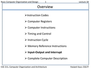
1. Basic Computer Orgsnization and Design 1 Lecture 18
CSE 211, Computer Organization and Architecture Harjeet Kaur, CSE/IT
Overview
Instruction Codes
Computer Registers
Computer Instructions
Timing and Control
Instruction Cycle
Memory Reference Instructions
Input-Output and Interrupt
Complete Computer Description
2. Basic Computer Orgsnization and Design 2 Lecture 18
CSE 211, Computer Organization and Architecture Harjeet Kaur, CSE/IT
Input/Output and Interrupt
Input-Output Configuration
INPR Input register - 8 bits
OUTR Output register - 8 bits
FGI Input flag - 1 bit
FGO Output flag - 1 bit
IEN Interrupt enable - 1 bit
- The terminal sends and receives serial information
- The serial info. from the keyboard is shifted into INPR
- The serial info. for the printer is stored in the OUTR
- INPR and OUTR communicate with the terminal serially and with the AC
in parallel.
- The flags are needed to synchronize the timing difference between I/O
device and the computer
A Terminal with a keyboard and a Printer
Input-output
terminal
Serial
communication
interface
Computer
registers and
flip-flops
Printer
Keyboard
Receiver
interface
Transmitter
interface
FGOOUTR
AC
INPR FGI
Serial Communications Path
Parallel Communications Path
3. Basic Computer Orgsnization and Design 3 Lecture 18
CSE 211, Computer Organization and Architecture Harjeet Kaur, CSE/IT
Programmed Controlled Data Transfer
loop: If FGI = 1 goto loop
INPR new data, FGI 1
loop: If FGO = 1 goto loop
consume OUTR, FGO 1
-- CPU -- -- I/O Device --
/* Input */ /* Initially FGI = 0 */
loop: If FGI = 0 goto loop
AC INPR, FGI 0
/* Output */ /* Initially FGO = 1 */
loop: If FGO = 0 goto loop
OUTR AC, FGO 0
Start Input
FGI 0
FGI=0
AC INPR
More
Character
END
Start Output
FGO 0
FGO=0
More
Character
OUTR AC
AC Data
yes
no
yes
no
FGI=0 FGO=1
yes
yes
no
no
4. Basic Computer Orgsnization and Design 4 Lecture 18
CSE 211, Computer Organization and Architecture Harjeet Kaur, CSE/IT
Input/Output Instructions
D7IT3 = p
IR(i) = Bi, i = 6, …, 11
p: SC 0 Clear SC
INP pB11: AC(0-7) INPR, FGI 0 Input char. to AC
OUT pB10: OUTR AC(0-7), FGO 0 Output char. from AC
SKI pB9: if(FGI = 1) then (PC PC + 1) Skip on input flag
SKO pB8: if(FGO = 1) then (PC PC + 1) Skip on output flag
ION pB7: IEN 1 Interrupt enable on
IOF pB6: IEN 0 Interrupt enable off
5. Basic Computer Orgsnization and Design 5 Lecture 18
CSE 211, Computer Organization and Architecture Harjeet Kaur, CSE/IT
Program controlled Input/Output
• Program-controlled I/O
- Continuous CPU involvement
I/O takes valuable CPU time
- CPU slowed down to I/O speed
- Simple
- Least hardware
Input
LOOP, SKI DEV
BUN LOOP
INP DEV
Output
LOOP, LDA DATA
LOP, SKO DEV
BUN LOP
OUT DEV
6. Basic Computer Orgsnization and Design 6 Lecture 18
CSE 211, Computer Organization and Architecture Harjeet Kaur, CSE/IT
Interrupt Initiated Input/Output
- Open communication only when some data has to be passed --> interrupt.
- The I/O interface, instead of the CPU, monitors the I/O device.
- When the interface founds that the I/O device is ready for data transfer,
it generates an interrupt request to the CPU
- Upon detecting an interrupt, the CPU stops momentarily the task
it is doing, branches to the service routine to process the data
transfer, and then returns to the task it was performing.
IEN (Interrupt-enable flip-flop)
- can be set and cleared by instructions
- when cleared, the computer cannot be interrupted
7. Basic Computer Orgsnization and Design 7 Lecture 18
CSE 211, Computer Organization and Architecture Harjeet Kaur, CSE/IT
Flow Chart of Interrupt Cycle
R = Interrupt f/f
- The interrupt cycle is a HW implementation of a branch and save return address
operation.
- At the beginning of the next instruction cycle, the instruction that is read from
memory is in address 1.
- At memory address 1, the programmer must store a branch instruction that sends
the control to an interrupt service routine
- The instruction that returns the control to the original program is "indirect BUN 0"
Store return address
R
=1=0
in location 0
M[0] PC
Branch to location 1
PC 1
IEN 0
R 0
Interrupt cycleInstruction cycle
Fetch and decode
instructions
IEN
FGI
FGO
Execute
instructions
R 1
=1
=1
=1
=0
=0
=0
8. Basic Computer Orgsnization and Design 8 Lecture 18
CSE 211, Computer Organization and Architecture Harjeet Kaur, CSE/IT
Register Transfer Operations in Interrupt Cycle
Register Transfer Statements for Interrupt Cycle
- R F/F 1 if IEN (FGI + FGO)T0T1T2
T0T1T2 (IEN)(FGI + FGO): R 1
- The fetch and decode phases of the instruction cycle
must be modified Replace T0, T1, T2 with R'T0, R'T1, R'T2
- The interrupt cycle :
RT0: AR 0, TR PC
RT1: M[AR] TR, PC 0
RT2: PC PC + 1, IEN 0, R 0, SC 0
After interrupt cycle
0 BUN 1120
0
1
PC = 256
255
1 BUN 0
Before interrupt
Main
Program
1120
I/O
Program
0 BUN 1120
0
PC = 1
256
255
1 BUN 0
Memory
Main
Program
1120
I/O
Program
256