Electrical Schematic Open Hardware PowerPC Notebook motherboard v. 0.4
•
0 j'aime•16,752 vues

Electrical Schematic Open Hardware PowerPC Notebook motherboard version May 2020 https://www.powerpc-notebook.org https://gitlab.com/power-progress-community/oshw-powerpc-notebook/powerpc-laptop-mobo/-/blob/master/PPC_notebook_electrical_schematics_v0.4.pdf

Recommandé
Recommandé
Contenu connexe
Tendances
Tendances (20)
Similaire à Electrical Schematic Open Hardware PowerPC Notebook motherboard v. 0.4
Similaire à Electrical Schematic Open Hardware PowerPC Notebook motherboard v. 0.4 (20)
Plus de Roberto Innocenti
Plus de Roberto Innocenti (7)
Dernier
Dernier (20)
Electrical Schematic Open Hardware PowerPC Notebook motherboard v. 0.4
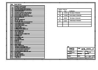
- 1. 1 1 2 2 3 3 4 4 5 5 A A B B C C D D Version Control Version V0.1 Date 2018/12 Modifications First release of Schematics Page Description 1 SCHEMATIC PAGE LISTING 2 3 SYSTEM BLOCK DIAGRAM 4 5 6 7 8 9 10 11 12 13 14 15 16 17 18 19 20 21 22 23 24 25 26 27 28 29 30 T2080 FIRST BANK DDR3L INTERFACE 31 32 T2080 IFC INTERFACE T2080 NOR and NAND FLASH INTERFACE T2080 SPI FLASH and SDHC INTERFACE T2080 SYSTEM LOGIC INTERFACE T2080 ETHERNET and SERDES INTERFACE T2080 USB INTERFACE 33 ACB_0001_0 SYSTEM POWER INPUT T2080 CORE POWER CONVERTOR SYSTEM CLOCK GENERATORs (cont.) MECHANICALs SYSTEM POWER CONVERTORs CPLD WRAPPER AND IO EXPANDER CHANGE LIST SYSTEM POWER CONVERTORs (cont.) SYSTEM CLOCK GENERATORs RGMII ETHERNET PORT 1 KEYBOARD INTERFACE KB_LED_AND_LED T2080 DUART and I2C DEVICE INTERFACE T2080 GROUND T2080 POWER SUPPLY (cont.) T2080 POWER SUPPLY ETHERNET PORT CONNECTOR SATA3 CONTROLLER SATA3 CONNECTORS USB3 CONTROLLER CONNECTORS USB3 CONTROLLER PCIE CONNECTORS PCIE BRIDGE 3G LTE MODEM PCIE BRIDGE POWER MXM PCIE MXM VIDEO OUT I2C WRAPPER AUDIO CMEDIA AUDIO CONNECTORS MAIN POWER BATTERY CHARGER 34 35 36 37 38 39 40 41 V0.2 2019/09 Second release of Schematics T2080 SECOND BANK DDR3L INTERFACE 42 43 USB_HUB V0.3 2020/04 Third release of Schematics 44 ETHERNET CARD V0.4 2020/05 Fourth release of Schematics Project Creation Date Last modify date Designed by: Controlled by: approved by: PCB Code BOM file Sheet of REV. Format Copyright (C) 2018-2020, Power Progress Community, Hardware Licensee is CERN Open Hardware Licence v1.2 Page title PAGE LISTING 0 B1 41 Monday, May 25, 2020 PROTO Project Creation Date Last modify date Designed by: Controlled by: approved by: PCB Code BOM file Sheet of REV. Format Copyright (C) 2018-2020, Power Progress Community, Hardware Licensee is CERN Open Hardware Licence v1.2 Page title PAGE LISTING 0 B1 41 Monday, May 25, 2020 PROTO Project Creation Date Last modify date Designed by: Controlled by: approved by: PCB Code BOM file Sheet of REV. Format Copyright (C) 2018-2020, Power Progress Community, Hardware Licensee is CERN Open Hardware Licence v1.2 Page title PAGE LISTING 0 B1 41 Monday, May 25, 2020 PROTO
- 2. 1 1 2 2 3 3 4 4 5 5 A A B B C C D D SYSTEM BLOCK DIAGRAM ACB_0001_0Project Creation Date Last modify date Designed by: Controlled by: approved by: PCB Code BOM file Sheet of REV. Format Copyright (C) 2018-2020, Power Progress Community, Hardware Licensee is CERN Open Hardware Licence v1.2 Page title BLOCK DIAGRAM 0 A02 41 Monday, May 25, 2020 PROTO Project Creation Date Last modify date Designed by: Controlled by: approved by: PCB Code BOM file Sheet of REV. Format Copyright (C) 2018-2020, Power Progress Community, Hardware Licensee is CERN Open Hardware Licence v1.2 Page title BLOCK DIAGRAM 0 A02 41 Monday, May 25, 2020 PROTO Project Creation Date Last modify date Designed by: Controlled by: approved by: PCB Code BOM file Sheet of REV. Format Copyright (C) 2018-2020, Power Progress Community, Hardware Licensee is CERN Open Hardware Licence v1.2 Page title BLOCK DIAGRAM 0 A02 41 Monday, May 25, 2020 PROTO
- 3. 1 1 2 2 3 3 4 4 5 5 A A B B C C D D T2080 DDR3L MEMORY INTERFACE 1.35V DDR3L SDRAM SODIMM 4GB (x64, DDR3L) SPD ADDR = 0x51 1G6 For DDR3L-1600 T2080 REV 1.0: 187 ohm 3V3 1V35 1V35 MVREF 1V35 1V35 1V35 VTT MVREF 1V35 3V3 VTT MVREF DDR_RST_N4,15 DDR_REFCLK 35 DDR_MBA[0..2]4 DDR_MA[0..15]4 DDR_MWE_N4 DDR_MCS2_N4 DDR_MCS3_N4 DDR_MCK2_P4 DDR_MCK2_N4 DDR_MCK3_P4 DDR_MCK3_N4 DDR_MCKE24 DDR_MCKE34 DDR_MCRAS_N4 DDR_MRAS_N4 DDR_MDM[0..8]4 DDR_DQ[0..63]4 DDR_MDQS0_P4 DDR_MDQS0_N4 DDR_MDQS1_P4 DDR_MDQS1_N4 DDR_MDQS2_P4 DDR_MDQS2_N4 DDR_MDQS3_P4 DDR_MDQS3_N4 DDR_MDQS4_P4 DDR_MDQS4_N4 DDR_MDQS5_P4 DDR_MDQS5_N4 DDR_MDQS6_P4 DDR_MDQS6_N4 DDR_MDQS7_P4 DDR_MDQS7_N4 I2C_DDR3_1_SCL32 I2C_DDR3_1_SDA32 DDR_MODT24 DDR_MODT34 Project Creation Date Last modify date Designed by: Controlled by: approved by: PCB Code BOM file Sheet of REV. Format Copyright (C) 2018-2020, Power Progress Community, Hardware Licensee is CERN Open Hardware Licence v1.2 Page title ACB_0001_0 3 41 Monday, May 25, 2020Saturday, April 20, 2013 A30 DDR3 <Author> <Approved by><Cheked by> PROTO Project Creation Date Last modify date Designed by: Controlled by: approved by: PCB Code BOM file Sheet of REV. Format Copyright (C) 2018-2020, Power Progress Community, Hardware Licensee is CERN Open Hardware Licence v1.2 Page title ACB_0001_0 3 41 Monday, May 25, 2020Saturday, April 20, 2013 A30 DDR3 <Author> <Approved by><Cheked by> PROTO Project Creation Date Last modify date Designed by: Controlled by: approved by: PCB Code BOM file Sheet of REV. Format Copyright (C) 2018-2020, Power Progress Community, Hardware Licensee is CERN Open Hardware Licence v1.2 Page title ACB_0001_0 3 41 Monday, May 25, 2020Saturday, April 20, 2013 A30 DDR3 <Author> <Approved by><Cheked by> PROTO M1 MT8KTF51264HZ-1G6 TP2 C10 0.1uF C22 0.1uF C8 0.1uF C15 0.1uF C12 0.1uF TP8 C16 0.1uF TP3 R3 187 1% C18 0.1uF TP9 C7 0.1uF R4 187 1% C23 0.1uF CONN204_DDR3_SODIMM NC NC VTT VTT VREFCA VREF/DQ VDDSPD VDD VDD VDD VDD VDD VDD VDD VDD VDD VDD VDD VDD VDD VDD VDD VDD VDD VDD GND GND GND GND GND GND GND GND GND GND GND GND GND GND GND GND GND GND GND GND GND GND GND GND GND GND GND GND GND GND GND GND GND GND GND GND GND GND GND GND GND GND GND GND GND GND GND GND GND GND GND GND J3F1B 2 OF 2 CONN E85705-003 1 2 3 8 9 13 14 19 20 25 26 31 32 37 38 43 44 48 49 54 55 60 61 65 66 71 72 75 76 77 81 82 87 88 93 94 99 100 105 106 111 112 117 118 122 123 124 126 127 128 133 134 138 139 144 145 150 151 155 156 161 162 167 168 172 173 178 179 184 185 189 190 195 196 199 203 204 C11 0.1uF C19 0.1uF TP1 C20 0.1uF R2 1K TP4 C6 0.1uF TP10 CONN204_DDR3_SODIMM A<12>/BC_N A<14> A<13> A<11> A<15>/BA3 A<10>/AP A<3>/A4 A<4>/A3 A<2> A<9> A<1> A<8>/A7 A<7>/A8 A<6>/A5 A<5>/A6 A<0> CK0P S0_N S1_N BA0/BA1 BA1/BA0 CK0N BA2 CKE1 CKE0 CAS_N RAS_N RST_N CK1P CK1N WE_N ODT1 ODT0 SCL SA1 SA0 SDA DQS0P DM0 DM1 DM2 DM3 DM4 DM5 DM7 DM6 DQS0N DQS4N DQS4P DQS1P DQS5P DQS1N DQS2P DQS2N DQS3P DQS3N DQS5N DQS6P DQS6N DQS7P DQS7N DQ<63> DQ<62> DQ<61> DQ<59> DQ<60> DQ<58> DQ<54> DQ<53> DQ<57> DQ<56> DQ<55> DQ<52> DQ<49> DQ<50> DQ<51> DQ<48> DQ<47> DQ<46> DQ<43> DQ<40> DQ<39> DQ<41> DQ<42> DQ<44> DQ<45> DQ<38> DQ<30> DQ<29> DQ<37> DQ<36> DQ<35> DQ<34> DQ<33> DQ<32> DQ<31> DQ<28> DQ<18> DQ<19> DQ<22> DQ<23> DQ<21> DQ<20> DQ<24> DQ<27> DQ<26> DQ<25> DQ<14> DQ<15> DQ<16> DQ<12> DQ<11> DQ<10> DQ<8> DQ<9> DQ<13> DQ<17> DQ<7> DQ<6> DQ<5> DQ<4> DQ<3> DQ<2> DQ<1> DQ<0> EVENT_N TEST J3F1A 1 OF 2 CONN E85705-003 4 5 6 7 10 11 12 15 16 17 18 21 22 23 24 27 28 29 30 33 34 35 36 39 40 41 42 45 46 47 50 51 52 53 56 57 58 59 62 63 64 67 68 69 70 73 74 78 79 80 83 84 85 86 89 90 91 92 95 96 97 98 101 102 103 104 107 108 109 110 113 114 115 116 119 120 121 125 129 130 131 132 135 136 137 140 141 142 143 146 147 148 149 152 153 154 157 158 159 160 163 164 165 166 169 170 171 174 175 176 177 180 181 182 183 186 187 188 191 192 193 194 197 198 200 201 202 TP5 C21 0.1uF C13 0.1uF TP11 TP6 C9 0.1uF C3 22uF C5 0.1uF C17 0.1uF DDR1 (G1VDD) OVDD G1VDD/2 U1I T2080 D1_MDQ00 B24 D1_MDQ01 A24 D1_MDQ02 C25 D1_MDQ03 D24 D1_MDQ04 D25 D1_MDQ05 C26 D1_MDQ06 B27 D1_MDQ07 C27 D1_MDQ08 H23 D1_MDQ09 G23 D1_MDQ10 F24 D1_MDQ11 F25 D1_MDQ12 E25 D1_MDQ13 E26 D1_MDQ14 D27 D1_MDQ15 G25 D1_MDQ16 J23 D1_MDQ17 H24 D1_MDQ18 H25 D1_MDQ19 J26 D1_MDQ20 J25 D1_MDQ21 J27 D1_MDQ22 H28 D1_MDQ23 K28 D1_MDQ24 L23 D1_MDQ25 M25 D1_MDQ26 K24 D1_MDQ27 K27 D1_MDQ28 M24 D1_MDQ29 L27 D1_MDQ30 M27 D1_MDQ31 M28 D1_MDQ32 T27 D1_MDQ33 V27 D1_MDQ34 U25 D1_MDQ35 U26 D1_MDQ36 R25 D1_MDQ37 T25 D1_MDQ38 T24 D1_MDQ39 U23 D1_MDQ40 Y28 D1_MDQ41 Y27 D1_MDQ42 Y25 D1_MDQ43 Y24 D1_MDQ44 V25 D1_MDQ45 Y23 D1_MDQ46 V24 D1_MDQ47 W23 D1_MDQ48 AA27 D1_MDQ49 AB28 D1_MDQ50 AB27 D1_MDQ51 AC27 D1_MDQ52 AB24 D1_MDQ53 AB23 D1_MDQ54 AA23 D1_MDQ55 AA25 D1_MDQ56 AD28 D1_MDQ57 AD27 D1_MDQ58 AE27 D1_MDQ59 AC25 D1_MDQ60 AF28 D1_MDQ61 AF27 D1_MDQ62 AG27 D1_MDQ63 AE26 D1_MECC0 N25 D1_MECC1 N23 D1_MECC2 N26 D1_MECC3 N27 D1_MECC4 R27 D1_MECC5 R26 D1_MECC6 R23 D1_MECC7 P24 D1_MAPAR_ERR_B E30 D1_MAPAR_OUT AA30 D1_MDM0 A25 D1_MDM1 E27 D1_MDM2 G26 D1_MDM3 K25 D1_MDM4 T28 D1_MDM5 W25 D1_MDM6 AA26 D1_MDM7 AJ27 D1_MDM8 P25 D1_MDQS0 A26 D1_MDQS1 F28 D1_MDQS2 G27 D1_MDQS3 L26 D1_MDQS4 V28 D1_MDQS5 W27 D1_MDQS6 AB25 D1_MDQS7 AH26 D1_MDQS8 P27 D1_MBA0 AC30 D1_MBA1 AA29 D1_MBA2 D28 D1_MA00 Y30 D1_MA01 W29 D1_MA02 M30 D1_MA03 L30 D1_MA04 L29 D1_MA05 J30 D1_MA06 J29 D1_MA07 G29 D1_MA08 H30 D1_MA09 F30 D1_MA10 AB30 D1_MA11 G30 D1_MA12 E29 D1_MA13 AG29 D1_MA14 D30 D1_MA15 C29 D1_MCS0_B AD30 D1_MCS1_B AH30 D1_MCS2_B AK28 D1_MCS3_B AJ28 D1_MCKE0 B29 D1_MCKE1 B28 D1_MCKE2 C30 D1_MCKE3 A28 D1_MCK0 P30 D1_MCK1 R30 D1_MCK2 U29 D1_MCK3 W30 D1_MCK0_B N30 D1_MCK1_B R29 D1_MCK2_B U30 D1_MCK3_B V30 D1_MODT0 AG30 D1_MODT1 AH29 D1_MODT2 AF30 D1_MODT3 AJ29 D1_MDIC0 K30D1_MDIC1 N29 D1_MCAS_B AE29 D1_MDQS0_B B25 D1_MDQS1_B F27 D1_MDQS2_B H27 D1_MDQS3_B L25 D1_MDQS4_B U27 D1_MDQS5_B W26 D1_MDQS6_B AC26 D1_MDQS7_B AH27 D1_MDQS8_B P28 D1_MRAS_B AC29 D1_MWE_B AE30 D1_MVREF F21 D1_DDRCLK E23 D1_TPA C23 C1 0.1uF C2 22uF R1 4.7K C4 22uF TP7 C14 0.1uF DDR_MCK0_P DDR_MCK0_N DDR_MCK1_P DDR_MCK1_N DDR_MBA0 DDR_MBA1 DDR_MBA2 DDR_MDQS0_P DDR_MDQS1_P DDR_MDQS2_P DDR_MDQS3_P DDR_MDQS5_P DDR_MDQS4_P DDR_MDQS6_P DDR_MDQS7_P DDR_MDQS0_N DDR_MDQS1_N DDR_MDQS2_N DDR_MDQS3_N DDR_MDQS5_N DDR_MDQS7_N DDR_MDQS6_N DDR_MDQS4_N DDR_MCS0_N DDR_MCS1_N DDR_MCRAS_N DDR_MRAS_N DDR_MWE_N DDR_MDM0 DDR_MDM1 DDR_MDM2 DDR_MDM3 DDR_MDM4 DDR_MDM5 DDR_MDM6 DDR_MDM7 DDR_MCKE0 DDR_MCKE1 DDR_MODT0 DDR_MODT1 DDR_MA[0..15] DDR_MDM[0..8] DDR_MBA[0..2] DDR_MCK1_P DDR_MCK1_N DDR_MCK0_P DDR_MCK0_N DDR_MDQS0_P DDR_MDQS1_P DDR_MDQS2_P DDR_MDQS3_P DDR_MDQS5_P DDR_MDQS4_P DDR_MDQS6_P DDR_MDQS7_P DDR_MDQS8_P DDR_MDQS0_N DDR_MDQS1_N DDR_MDQS2_N DDR_MDQS3_N DDR_MDQS5_N DDR_MDQS7_N DDR_MDQS6_N DDR_MDQS4_N DDR_MDQS8_N DDR_MBA0 DDR_MBA1 DDR_MBA2 DDR_MA0 DDR_MA1 DDR_MA2 DDR_MA3 DDR_MA4 DDR_MA5 DDR_MA6 DDR_MA7 DDR_MA8 DDR_MA9 DDR_MA10 DDR_MA11 DDR_MA12 DDR_MA13 DDR_MA14 DDR_MA15 DDR_MDM0 DDR_MDM1 DDR_MDM2 DDR_MDM3 DDR_MDM4 DDR_MDM5 DDR_MDM6 DDR_MDM7 DDR_MDM8 DDR_MCKE0 DDR_MCKE1 DDR_MDM[0..8] DDR_MBA[0..2] DDR_MA[0..15] DDR_MCS0_N DDR_MCS1_N DDR_MODT0 DDR_MODT1 DDR_MRAS_N DDR_MCRAS_N DDR_MWE_N DDR_ECC0 DDR_ECC1 DDR_ECC2 DDR_ECC3 DDR_ECC4 DDR_ECC5 DDR_ECC6 DDR_ECC7 DDR_DQ0 DDR_DQ1 DDR_DQ2 DDR_DQ3 DDR_DQ4 DDR_DQ5 DDR_DQ6 DDR_DQ7 DDR_DQ8 DDR_DQ9 DDR_DQ10 DDR_DQ11 DDR_DQ12 DDR_DQ13 DDR_DQ14 DDR_DQ15 DDR_DQ16 DDR_DQ17 DDR_DQ18 DDR_DQ19 DDR_DQ20 DDR_DQ21 DDR_DQ22 DDR_DQ23 DDR_DQ24 DDR_DQ25 DDR_DQ26 DDR_DQ27 DDR_DQ28 DDR_DQ29 DDR_DQ30 DDR_DQ31 DDR_DQ32 DDR_DQ33 DDR_DQ34 DDR_DQ35 DDR_DQ36 DDR_DQ37 DDR_DQ38 DDR_DQ39 DDR_DQ40 DDR_DQ41 DDR_DQ42 DDR_DQ43 DDR_DQ44 DDR_DQ45 DDR_DQ46 DDR_DQ47 DDR_DQ48 DDR_DQ49 DDR_DQ50 DDR_DQ51 DDR_DQ52 DDR_DQ53 DDR_DQ54 DDR_DQ55 DDR_DQ56 DDR_DQ57 DDR_DQ58 DDR_DQ59 DDR_DQ60 DDR_DQ61 DDR_DQ62 DDR_DQ63 DDR_DQ[0..63] DDR_DQ62 DDR_DQ63 DDR_DQ60 DDR_DQ61 DDR_DQ58 DDR_DQ59 DDR_DQ56 DDR_DQ57 DDR_DQ54 DDR_DQ55 DDR_DQ52 DDR_DQ53 DDR_DQ50 DDR_DQ51 DDR_DQ48 DDR_DQ49 DDR_DQ46 DDR_DQ47 DDR_DQ44 DDR_DQ45 DDR_DQ42 DDR_DQ43 DDR_DQ40 DDR_DQ41 DDR_DQ38 DDR_DQ39 DDR_DQ36 DDR_DQ37 DDR_DQ34 DDR_DQ35 DDR_DQ32 DDR_DQ33 DDR_DQ30 DDR_DQ31 DDR_DQ28 DDR_DQ29 DDR_DQ26 DDR_DQ27 DDR_DQ24 DDR_DQ25 DDR_DQ22 DDR_DQ23 DDR_DQ20 DDR_DQ21 DDR_DQ18 DDR_DQ19 DDR_DQ16 DDR_DQ17 DDR_DQ14 DDR_DQ15 DDR_DQ12 DDR_DQ13 DDR_DQ10 DDR_DQ11 DDR_DQ8 DDR_DQ9 DDR_DQ6 DDR_DQ7 DDR_DQ4 DDR_DQ5 DDR_DQ2 DDR_DQ3 DDR_DQ0 DDR_DQ1 DDR_DQ[0..63] DDR_MA0 DDR_MA1 DDR_MA2 DDR_MA3 DDR_MA4 DDR_MA5 DDR_MA6 DDR_MA7 DDR_MA8 DDR_MA9 DDR_MA10 DDR_MA11 DDR_MA12 DDR_MA13 DDR_MA14 DDR_MA15 DDR_MDM8 DDR_MDQS8_P DDR_MDQS8_N DDR_MCS2_N DDR_MCS3_N DDR_MCKE2 DDR_MCKE3 DDR_MCK2_P DDR_MCK2_N DDR_MCK3_P DDR_MCK3_N DDR_MODT2 DDR_MODT3 DDR_MDM[0..8] DDR_MBA[0..2] DDR_MA[0..15] DDR_MCS2_N DDR_MCS3_N DDR_MCKE2 DDR_MCKE3 DDR_MCK2_P DDR_MCK2_N DDR_MCK3_P DDR_MCK3_N DDR_DQ[0..63] DDR_MCRAS_N DDR_MRAS_N DDR_MWE_N DDR_MDQS0_P DDR_MDQS0_N DDR_MDQS1_P DDR_MDQS1_N DDR_MDQS2_P DDR_MDQS2_N DDR_MDQS3_P DDR_MDQS3_N DDR_MDQS4_P DDR_MDQS4_N DDR_MDQS5_P DDR_MDQS5_N DDR_MDQS6_P DDR_MDQS6_N DDR_MDQS7_P DDR_MDQS7_N DDR_MODT2 DDR_MODT3
- 4. 1 1 2 2 3 3 4 4 5 5 A A B B C C D D SPD ADDR = 0x52 4GB (x64, DDR3L) 1.35V DDR3L SDRAM SODIMM 1G6 For DDR3L-1600 1V35 3V3 MVREF VTT 1V35 VTT MVREF 1V35 1V35 3V3 DDR_RST_N3,15 DDR_MA[0..15]3 DDR_MBA[0..2]3 DDR_MCS2_N3 DDR_MCS3_N3 DDR_MCK2_P3 DDR_MCK2_N3 DDR_MCK3_P3 DDR_MCK3_N3 DDR_MCKE23 DDR_MCKE33 DDR_MCRAS_N3 DDR_MRAS_N3 DDR_MWE_N3 DDR_MDM[0..8]3 DDR_DQ[0..63] 3 DDR_MDQS0_P3 DDR_MDQS0_N3 DDR_MDQS1_P3 DDR_MDQS1_N3 DDR_MDQS2_P3 DDR_MDQS2_N3 DDR_MDQS3_P3 DDR_MDQS3_N3 DDR_MDQS4_P3 DDR_MDQS4_N3 DDR_MDQS5_P3 DDR_MDQS5_N3 DDR_MDQS6_P3 DDR_MDQS6_N3 DDR_MDQS7_P3 DDR_MDQS7_N3 I2C_DDR3_2_SCL32 I2C_DDR3_2_SDA32 DDR_MODT23 DDR_MODT33 Project Creation Date Last modify date Designed by: Controlled by: approved by: PCB Code BOM file Sheet of REV. Format Copyright (C) 2018-2020, Power Progress Community, Hardware Licensee is CERN Open Hardware Licence v1.2 Page title ACB_0001_0 3 41 Monday, May 25, 2020Sunday, September 22, 2019 A30 DDR3_2 <Author> <Approved by><Cheked by> PROTO Project Creation Date Last modify date Designed by: Controlled by: approved by: PCB Code BOM file Sheet of REV. Format Copyright (C) 2018-2020, Power Progress Community, Hardware Licensee is CERN Open Hardware Licence v1.2 Page title ACB_0001_0 3 41 Monday, May 25, 2020Sunday, September 22, 2019 A30 DDR3_2 <Author> <Approved by><Cheked by> PROTO Project Creation Date Last modify date Designed by: Controlled by: approved by: PCB Code BOM file Sheet of REV. Format Copyright (C) 2018-2020, Power Progress Community, Hardware Licensee is CERN Open Hardware Licence v1.2 Page title ACB_0001_0 3 41 Monday, May 25, 2020Sunday, September 22, 2019 A30 DDR3_2 <Author> <Approved by><Cheked by> PROTO R938 1K C1111 0.1uF C1092 22uF C1093 22uF C1094 0.1uF C1095 0.1uF C1096 0.1uF M16 MT8KTF51264HZ-1G6 C1098 0.1uF C1097 0.1uF C1099 0.1uF C1105 0.1uF C1100 0.1uF CONN204_DDR3_SODIMM NC NC VTT VTT VREFCA VREF/DQ VDDSPD VDD VDD VDD VDD VDD VDD VDD VDD VDD VDD VDD VDD VDD VDD VDD VDD VDD VDD GND GND GND GND GND GND GND GND GND GND GND GND GND GND GND GND GND GND GND GND GND GND GND GND GND GND GND GND GND GND GND GND GND GND GND GND GND GND GND GND GND GND GND GND GND GND GND GND GND GND GND GND J3F2B 2 OF 2 CONN E85705-003 1 2 3 8 9 13 14 19 20 25 26 31 32 37 38 43 44 48 49 54 55 60 61 65 66 71 72 75 76 77 81 82 87 88 93 94 99 100 105 106 111 112 117 118 122 123 124 126 127 128 133 134 138 139 144 145 150 151 155 156 161 162 167 168 172 173 178 179 184 185 189 190 195 196 199 203 204 C1106 0.1uF C1101 0.1uF C1107 0.1uF CONN204_DDR3_SODIMM A<12>/BC_N A<14> A<13> A<11> A<15>/BA3 A<10>/AP A<3>/A4 A<4>/A3 A<2> A<9> A<1> A<8>/A7 A<7>/A8 A<6>/A5 A<5>/A6 A<0> CK0P S0_N S1_N BA0/BA1 BA1/BA0 CK0N BA2 CKE1 CKE0 CAS_N RAS_N RST_N CK1P CK1N WE_N ODT1 ODT0 SCL SA1 SA0 SDA DQS0P DM0 DM1 DM2 DM3 DM4 DM5 DM7 DM6 DQS0N DQS4N DQS4P DQS1P DQS5P DQS1N DQS2P DQS2N DQS3P DQS3N DQS5N DQS6P DQS6N DQS7P DQS7N DQ<63> DQ<62> DQ<61> DQ<59> DQ<60> DQ<58> DQ<54> DQ<53> DQ<57> DQ<56> DQ<55> DQ<52> DQ<49> DQ<50> DQ<51> DQ<48> DQ<47> DQ<46> DQ<43> DQ<40> DQ<39> DQ<41> DQ<42> DQ<44> DQ<45> DQ<38> DQ<30> DQ<29> DQ<37> DQ<36> DQ<35> DQ<34> DQ<33> DQ<32> DQ<31> DQ<28> DQ<18> DQ<19> DQ<22> DQ<23> DQ<21> DQ<20> DQ<24> DQ<27> DQ<26> DQ<25> DQ<14> DQ<15> DQ<16> DQ<12> DQ<11> DQ<10> DQ<8> DQ<9> DQ<13> DQ<17> DQ<7> DQ<6> DQ<5> DQ<4> DQ<3> DQ<2> DQ<1> DQ<0> EVENT_N TEST J3F2A 1 OF 2 CONN E85705-003 4 5 6 7 10 11 12 15 16 17 18 21 22 23 24 27 28 29 30 33 34 35 36 39 40 41 42 45 46 47 50 51 52 53 56 57 58 59 62 63 64 67 68 69 70 73 74 78 79 80 83 84 85 86 89 90 91 92 95 96 97 98 101 102 103 104 107 108 109 110 113 114 115 116 119 120 121 125 129 130 131 132 135 136 137 140 141 142 143 146 147 148 149 152 153 154 157 158 159 160 163 164 165 166 169 170 171 174 175 176 177 180 181 182 183 186 187 188 191 192 193 194 197 198 200 201 202 C1102 0.1uF C1108 0.1uF C1103 0.1uF C1109 0.1uF C1104 0.1uF C1090 0.1uF C1110 0.1uF C1091 22uF DDR_MA[0..15] DDR_DQ[0..63] DDR_MA15 DDR_DQ63 DDR_MA14 DDR_DQ62 DDR_MA13 DDR_DQ61 DDR_MA12 DDR_DQ60 DDR_MA11 DDR_DQ59 DDR_MA10 DDR_DQ58 DDR_MA9 DDR_DQ57 DDR_MA8 DDR_DQ56 DDR_MA7 DDR_DQ55 DDR_MA6 DDR_DQ54 DDR_MA5 DDR_DQ53 DDR_MA4 DDR_DQ52 DDR_MA3 DDR_DQ51 DDR_MA2 DDR_DQ50 DDR_MA1 DDR_DQ49 DDR_MA0 DDR_DQ48 DDR_MBA[0..2] DDR_DQ47 DDR_MBA0 DDR_DQ46 DDR_MBA1 DDR_DQ45 DDR_MBA2 DDR_DQ44 DDR_DQ43 DDR_DQ42 DDR_DQ41 DDR_DQ40 DDR_DQ39 DDR_DQ38 DDR_DQ37 DDR_DQ36 DDR_DQ35 DDR_DQ34 DDR_DQ33 DDR_DQ32 DDR_MCRAS_N DDR_DQ31 DDR_MRAS_N DDR_DQ30 DDR_DQ29 DDR_MWE_N DDR_DQ28 DDR_DQ27 DDR_DQ26 DDR_DQ25 DDR_DQ24 DDR_DQ23 DDR_DQ22 DDR_DQ21 DDR_DQ20 DDR_DQ19 DDR_MDM[0..8] DDR_DQ18 DDR_MDM0 DDR_DQ17 DDR_MDM1 DDR_DQ16 DDR_MDM2 DDR_DQ15 DDR_MDM3 DDR_DQ14 DDR_MDM4 DDR_DQ13 DDR_MDM5 DDR_DQ12 DDR_MDM6 DDR_DQ11 DDR_MDM7 DDR_DQ10 DDR_DQ9 DDR_MDQS0_P DDR_DQ8 DDR_MDQS0_N DDR_DQ7 DDR_MDQS1_P DDR_DQ6 DDR_MDQS1_N DDR_DQ5 DDR_MDQS2_P DDR_DQ4 DDR_MDQS2_N DDR_DQ3 DDR_MDQS3_P DDR_DQ2 DDR_MDQS3_N DDR_DQ1 DDR_MDQS4_P DDR_DQ0 DDR_MDQS4_N DDR_MDQS5_P DDR_MDQS5_N DDR_MDQS6_P DDR_MDQS6_N DDR_MDQS7_P DDR_MDQS7_N DDR_MCS2_N DDR_MCS3_N DDR_MCKE2 DDR_MCKE3 DDR_MCK2_P DDR_MCK2_N DDR_MCK3_P DDR_MCK3_N DDR_MODT2 DDR_MODT3
- 5. 1 1 2 2 3 3 4 4 5 5 A A B B C C D D T2080 IFC INTERFACE cfg_rcw_src0 cfg_rcw_src1 cfg_rcw_src2 cfg_rcw_src3 cfg_rcw_src4 cfg_rcw_src5 cfg_rcw_src6 cfg_rcw_src7 cfg_rcw_src8 cfg_ifc_te cfg_pll_config_sel_b cfg_por_ainit cfg_svr0 cfg_svr1 cfg_dram_type cfg_rsp_dis 0_0010_0111: NOR FLASH BOOT 0_0100_0000: SD CARD BOOT 0_0100_0101: SPI BOOT 1_0001_1001: NAND FLASH BOOT For T2080 1: DDR3L 1: TE logic 0 cfg_rcw_src[0:8] cfg_dram_type T2080 RESET CONFIGURATION CS0: NOR or NAND CS1: NAND or NOR CS2: CPLD cfg_test_port_dis ACB_0001_0 1V8 1V8 1V8 1V8 1V81V8 1V8 IFC_AD[0..15] 6 IFC_WE_N 6 IFC_CS0_N 15 IFC_CS1_N 15 IFC_CS2_N 15 IFC_CLE 6 IFC_OE_N 6 IFC_RB0_N 15 IFC_RB1_N 15 IFC_WP_N 6 IFC_AVD 6 IFC_NDWE_N 6 IFC_CLK 15 IFC_A[5..31] 5,6 IFC_A[5..31] 5,6 GPIO2_10 15 GPIO1_9 15 GPIO1_10 15 GPIO1_11 15 GPIO1_12 15 GPIO2_13 15 GPIO2_14 15 Project Creation Date Last modify date Designed by: Controlled by: approved by: PCB Code BOM file Sheet of REV. Format Copyright (C) 2018-2020, Power Progress Community, Hardware Licensee is CERN Open Hardware Licence v1.2 Page title IFC 0 A34 41 Monday, May 25, 2020 PROTO Project Creation Date Last modify date Designed by: Controlled by: approved by: PCB Code BOM file Sheet of REV. Format Copyright (C) 2018-2020, Power Progress Community, Hardware Licensee is CERN Open Hardware Licence v1.2 Page title IFC 0 A34 41 Monday, May 25, 2020 PROTO Project Creation Date Last modify date Designed by: Controlled by: approved by: PCB Code BOM file Sheet of REV. Format Copyright (C) 2018-2020, Power Progress Community, Hardware Licensee is CERN Open Hardware Licence v1.2 Page title IFC 0 A34 41 Monday, May 25, 2020 PROTO R46 33 U2 74LVC16373 1Q1 2 1Q2 3 1Q3 5 1Q4 6 1Q5 8 1Q6 9 1Q7 11 1Q8 12 1D1 47 1D2 46 1D3 44 1D4 43 1D5 41 1D6 40 1D7 38 1D8 37 2D1 36 2D2 35 2D3 33 2D4 32 2D5 30 2D6 29 2D7 27 2D8 26 LE1 48 OE1 1 LE2 25 OE2 24 2Q1 13 2Q2 14 2Q3 16 2Q4 17 2Q5 19 2Q6 20 2Q7 22 2Q8 23 GND 4 GND 10 GND 15 GND 21 GND 28 GND 45GND 39GND 34VCC 7 VCC 18 VCC 31 VCC 42 ON SW2 SWITCH_DIP_8 1 1 2 2 3 3 4 4 5 5 6 6 7 7 8 8 9 910 1011 1112 1213 1314 1415 1516 16 R32 4.7K R5 4.7K R48 10 R36 33 R19 4.7K R20 20K R33 4.7K R47 4.7K R37 33 R23 4.7K R12 20K R7 4.7K R40 33 R35 33 C24 0.1uF R38 4.7K R10 20K R24 4.7K R34 33 R9 4.7K R42 33 R8 20K C25 0.1uF R41 33 R25 4.7K R6 20K R16 20K R11 4.7K R39 4.7K R14 20K IFC (OVDD) U1C T2080 IFC_AD00 A13 IFC_AD01 G13 IFC_AD02 C14 IFC_AD03 D13 IFC_AD04 A15 IFC_AD05 F13 IFC_AD06 E14 IFC_AD07 J13 IFC_AD08 E13 IFC_AD09 F14 IFC_AD10 H14 IFC_AD11 A14 IFC_AD12 C13 IFC_AD13 B15 IFC_AD14 F15 IFC_AD15 D14 IFC_PAR0 F18 IFC_PAR1 A17 IFC_A16 G15 IFC_A17 C15 IFC_A18 D15 IFC_A19 G14 IFC_A20 A16 IFC_A21 B14 IFC_A22 J15 IFC_A23 B18 IFC_A24 C16 IFC_A25 E17 IFC_A26 D16 IFC_A27 G17 IFC_A28 F16 IFC_A29 G16 IFC_A30 B21 IFC_A31 E16 IFC_CS0_B H16 IFC_CS1_B F17 IFC_CS2_B D19 IFC_CS3_B B17 IFC_CS4_B E19 IFC_CS5_B C18 IFC_CS6_B D21 IFC_CS7_B G19 IFC_WE0_B D17 IFC_BCTL H18 IFC_AVD C17 IFC_CLE H19 IFC_OE_B G18 IFC_WP0_B A18 IFC_RB0_B J17 IFC_PERR_B F19 IFC_CLK0 A22 IFC_CLK1 B20 IFC_TE A19 IFC_NDDQS J19 IFC_NDDDR_CLK D18 IFC_RB1_B C19 R13 4.7K R43 33 TP156 C27 0.1uF R26 4.7K R31 4.7K R21 20K R44 33 R22 4.7K DNP R27 4.7K ON SW1 SWITCH_DIP_8 1 1 2 2 3 3 4 4 5 5 6 6 7 7 8 8 9 910 1011 1112 1213 1314 1415 1516 16 C26 0.1uF R15 4.7K R45 33 R28 4.7K R29 4.7K R17 4.7K R18 20K R30 4.7K IFC_AD8 IFC_AD9 IFC_AD10 IFC_AD11 IFC_AD12 IFC_AD13 IFC_AD14 IFC_AD15 IFC_CLE IFC_TE IFC_A18 IFC_A19 IFC_A16 IFC_A17 IFC_A21 IFC_AVD IFC_AD0 IFC_AD1 IFC_AD2 IFC_AD3 IFC_AD4 IFC_AD5 IFC_AD6 IFC_AD7 IFC_AD8 IFC_AD9 IFC_AD10 IFC_AD11 IFC_AD12 IFC_AD13 IFC_AD14 IFC_AD15 IFC_A16 IFC_A17 IFC_A18 IFC_A19 IFC_A20 IFC_A21 IFC_A22 IFC_A23 IFC_A24 IFC_A25 IFC_A26 IFC_A27 IFC_A28 IFC_A29 IFC_A30 IFC_A31 IFC_TE IFC_AD5 IFC_AD6 IFC_AD7 IFC_AD8 IFC_AD9 IFC_AD10 IFC_AD11 IFC_AD12 IFC_AD13 IFC_AD14 IFC_AD15 IFC_A5 IFC_A6 IFC_A7 IFC_A8 IFC_A9 IFC_A10 IFC_A11 IFC_A12 IFC_A13 IFC_A14 IFC_A15 IFC_A16 IFC_A17 IFC_A18 IFC_A19 IFC_AVD IFC_OE_N IFC_WE_N IFC_WP_N IFC_A20 IFC_A31
- 6. 1 1 2 2 3 3 4 4 5 5 A A B B C C D D 128MB 16-BIT NOR FLASH T2080 NOR and NAND FLASH INTERFACE 512MB 8-BIT NAND FLASH ACB_0001_0 1V8 1V8 1V8 1V8 3V3 1V8 1V8 1V8 1V8 1V8 1V8 1V8 1V8 3V31V8 1V8 1V8 IFC_A[5..31]5 IFC_AD[0..15] 5,6 NOR_CS_N15 IFC_OE_N5,6 IFC_WE_N5 NOR_RST_N15 CFG_VBANK[0..2]15 IFC_AVD5 NAND_RB_N 15 NAND_CS_N15 IFC_CLE5 IFC_OE_N5,6 IFC_WP_N5 IFC_NDWE_N5 IFC_AD[0..15] 5,6 Project Creation Date Last modify date Designed by: Controlled by: approved by: PCB Code BOM file Sheet of REV. Format Copyright (C) 2018-2020, Power Progress Community, Hardware Licensee is CERN Open Hardware Licence v1.2 Page title FLASH 0 A35 41 Monday, May 25, 2020 PROTO Project Creation Date Last modify date Designed by: Controlled by: approved by: PCB Code BOM file Sheet of REV. Format Copyright (C) 2018-2020, Power Progress Community, Hardware Licensee is CERN Open Hardware Licence v1.2 Page title FLASH 0 A35 41 Monday, May 25, 2020 PROTO Project Creation Date Last modify date Designed by: Controlled by: approved by: PCB Code BOM file Sheet of REV. Format Copyright (C) 2018-2020, Power Progress Community, Hardware Licensee is CERN Open Hardware Licence v1.2 Page title FLASH 0 A35 41 Monday, May 25, 2020 PROTO C28 0.1uF JS28F00AM29EWHA U3 A0 31 A1 26 A2 25 A3 24 A4 23 A5 22 A6 21 A7 20 A8 10 A9 9 A10 8 A11 7 A12 6 A13 5 A14 4 A15 3 A16 54 A17 19 A18 18 A19 11 A20 12 A21 15 A22 2 A23 1 A24 56 CE 32 RESET 14 VIO 29 WE 13 OE 34 BYTE 53 WP/ACC 16 A25 55 VCC 43 NC2 28NC1 27 DQ0 35 DQ1 37 DQ2 39 DQ3 41 DQ4 44 DQ5 46 DQ6 48 DQ7 50 DQ8 36 DQ9 38 DQ10 40 DQ11 42 DQ12 45 DQ13 47 DQ14 49 DQ15/A-1 51 RDY/BUSY 17 GND 33 GND 52 NC3 30 U4B MT29F4G08ABBDAH4 NC1 H6 NC2 H7 NC3 J3 NC4 J5 NC5 D6 NC6 D7 NC7 D8 NC8 E3 NC9 E4 NC10 E5 NC11 E6 NC12 E7 NC13 E8 NC14 F3 NC15 F4 NC16 F5 NC17 F6 NC18 F8 NC19 G6 NC20 G7 NC21 H3 NC22 H5 DNU1 G3 DNU2 G8 NC23 A1 NC24 A2 NC25 B1 NC26 A9 NC27 A10 NC28 B9 NC29 B10 NC30 L1 NC31 L2 NC32 M1 NC33 M2 NC34 L9 NC35 L10 NC36 M9 NC37 M10 R49 4.7K C31 0.1uF U4A MT29F4G08ABBDAH4 CLE D5 ALE C4 CE C6 RE D4 WE C7 WP C3 R/B C8 LOCK G5 I/O0 H4 I/O1 J4 I/O2 K4 I/O3 K5 I/O4 K6 I/O5 J7 I/O6 K7 I/O7 J8 VSS K8VSS K3VSS F7VSS C5 VCC J6 VCC H8 VCC G4 VCC D3 C32 0.1uF U7 SN74LVC1G86 I0 1 I1 2 O 4VCC 5 GND 3 R53 4.7K R54 4.7K R50 4.7K U5 SN74LVC1G86 I0 1 I1 2 O 4VCC 5 GND 3 C29 0.1uFU6 SN74LVC1G86 I0 1 I1 2 O 4VCC 5 GND 3 C35 1uF C30 0.1uF R51 4.7K C33 0.1uF C34 0.1uF R52 4.7K R55 1K C37 0.1uF C36 0.1uF IFC_A8 IFC_A9 IFC_A10 IFC_A11 IFC_A12 IFC_A13 IFC_A14 IFC_A15 IFC_A16 IFC_A17 IFC_A18 IFC_A19 IFC_A20 IFC_A21 IFC_A22 IFC_A23 IFC_A24 IFC_A25 IFC_A26 IFC_A27 IFC_A28 IFC_A29 IFC_A30 IFC_AD0 IFC_AD1 IFC_AD2 IFC_AD3 IFC_AD4 IFC_AD5 IFC_AD6 IFC_AD7 IFC_AD8 IFC_AD9 IFC_AD10 IFC_AD11 IFC_AD12 IFC_AD13 IFC_AD14 IFC_AD15 CFG_VBANK2 IFC_A7 CFG_VBANK1 IFC_A6 CFG_VBANK0 IFC_A5 IFC_VA7 IFC_VA6 IFC_VA5 IFC_AD0 IFC_AD1 IFC_AD2 IFC_AD3 IFC_AD4 IFC_AD5 IFC_AD6 IFC_AD7
- 7. 1 1 2 2 3 3 4 4 5 5 A A B B C C D D CO-LAYOUT 64MB SERIAL FLASH T2080 SPI FLASH and SDHC INTERFACE TF CARD LABEL = TF CARD VOLTAGE ACB_0001_0 3V3 3V3 VDD_TF VDD_TF 3V3 VDD_TF 3V3 3V31V8 3V3 3V3 3V3 1V8 VDD_TF 1V8 3V3 1V8 VDD_TF 1V8 VDD_TF 1V8 1V8 VDD_TF 3V3 VDD_TF 1V8 GPIO2_1 15 GPIO2_2 15 GPIO2_3 15 PROC_SPI_MISO15 PROC_SPI_MOSI15 PROC_SPI_CLK15 Project Creation Date Last modify date Designed by: Controlled by: approved by: PCB Code BOM file Sheet of REV. Format Copyright (C) 2018-2020, Power Progress Community, Hardware Licensee is CERN Open Hardware Licence v1.2 Page title SPI&SDHC 0 A36 41 Monday, May 25, 2020 PROTO Project Creation Date Last modify date Designed by: Controlled by: approved by: PCB Code BOM file Sheet of REV. Format Copyright (C) 2018-2020, Power Progress Community, Hardware Licensee is CERN Open Hardware Licence v1.2 Page title SPI&SDHC 0 A36 41 Monday, May 25, 2020 PROTO Project Creation Date Last modify date Designed by: Controlled by: approved by: PCB Code BOM file Sheet of REV. Format Copyright (C) 2018-2020, Power Progress Community, Hardware Licensee is CERN Open Hardware Licence v1.2 Page title SPI&SDHC 0 A36 41 Monday, May 25, 2020 PROTO J1 JMP3 2 3 1 R63 20K C43 0.1uF R60 33 R58 20K C39 0.1uF U8 TXBN0304RSV A1 1 A2 2 A3 3 A4 4 NC1 5 GND 6 GND 7 OE 8 B4 9B3 10B2 11B1 12 VCCB 13 VCCA 16 NC2 14 NC3 15 U12 TXBN0304RSV A1 1 A2 2 A3 3 A4 4 NC1 5 GND 6 GND 7 OE 8 B4 9B3 10B2 11B1 12 VCCB 13 VCCA 16 NC2 14 NC3 15 R67 20K U11 N25Q512A13GF840F DNP CS 1 SO 2 WP 3 GND 4 SI 5 SCK 6 HOLD 7 VCC 8 EPAD 9 eSPI/SDHC(CVDD) SDHC(OVDD) U1M T2080 SPI_MOSI C1SPI_MISO C2 SPI_CLK B2 SPI_CS0_B/SDHC_DAT4 E3 SPI_CS1_B/SDHC_DAT5 K6 SPI_CS2_B/SDHC_DAT6 H5 SPI_CS3_B/SDHC_DAT7 L6 SDHC_CMD A3 SDHC_DAT0 D2 SDHC_DAT1 D3 SDHC_DAT2 H6 SDHC_DAT3 G5 SDHC_CLK C4 SDHC_CD_B E4 SDHC_WP F4 R61 10 R57 20K R72 33 R56 20K C41 0.1uF C46 0.1uF C42 0.1uF R69 4.7K DNP J2 TF_CONN_CD D3/CS 2 CMD/DIN 3 VDD 4 CLK/SCLK 5 VSS 6 D0/DOUT 7 D1/RSV 8 D2/RSV 1 MP3 12MP2 11MP1 10 MP4 13 CD 9 C45 0.1uF R70 4.7K R65 20K C40 1uF U9 N25Q512A13GSF40F CS 7 SO 8 WP 9 GND 10 SI 15 SCK 16 HOLD 1 VCC 2 NC1 3 NC2 4 NC3 5 NC4 6 NC5 11 NC6 12 NC7 13 NC8 14 R66 20K R64 20K R71 4.7K R62 10 R59 4.7K R68 20K C38 1uF U13 RClamp0524J.TCT 1 2 9 3 4 5 6 7 8 C47 0.1uF U14 RClamp0524J.TCT 1 2 9 3 4 5 6 7 8 C44 0.1uF U10 TXBN0304RSV A1 1 A2 2 A3 3 A4 4 NC1 5 GND 6 GND 7 OE 8 B4 9B3 10B2 11B1 12 VCCB 13 VCCA 16 NC2 14 NC3 15 PROC_SPI_MISO PROC_SPI_MOSI PROC_SPI_CLK PROC_SPI_CS0_N SDHC_CMD SDHC_CLK SDHC_CD_N SDHC_DAT2 SDHC_DAT0 SDHC_DAT1 SDHC_DAT3 SDHC_WP
- 8. 1 1 2 2 3 3 4 4 5 5 A A B B C C D D T2080 SYSTEM LOGIC INTERFACE cfg_test_port_mux_sel cfg_xvdd_sel XVDD use 1.35V TEST_SEL_B FOR T2080, PULL-UP ACB_0001_0 1V83V3 1V8 1V81V8 1V8 1V83V3 1V8 3V3 1V8 3V3 3V3 3V3 3V3 1V8 1V8 2V5 2V5 1V81V8 3V3 3V32V5 2V5 2V5 2V5 2V5 3V3 1V8 3V3 1V8 2V5 3V3 2V5 2V5 3V3 2V5 3V3 2V5 3V3 3V3 3V3 3V3 3V3 2V53V33V3 SYS_REFCLK35 IRQ08 15 IRQ09 15 IRQ00 15 IRQ01 15 IRQ02 15 RTC_INT_N 14 EC1_INT_N 19 EC1_PME_N 19 LP_TMPDET_N 42 TEMP_DIODE_P 14 TEMP_DIODE_N 14 I2C1_SCL 14,32,36,37 I2C1_SDA 14,32,36,37 I2C2_SCL 32 I2C2_SDA 32 I2C3_SCL 32 I2C3_SDA 32 I2C4_SCL32 I2C4_SDA32 PORESET_N15 HRESET_N15 RESET_REQ_N15 GPIO4_415 GPIO4_515 GPIO4_615 Project Creation Date Last modify date Designed by: Controlled by: approved by: PCB Code BOM file Sheet of REV. Format Copyright (C) 2018-2020, Power Progress Community, Hardware Licensee is CERN Open Hardware Licence v1.2 Page title SYS 0 A37 41 Monday, May 25, 2020 PROTO Project Creation Date Last modify date Designed by: Controlled by: approved by: PCB Code BOM file Sheet of REV. Format Copyright (C) 2018-2020, Power Progress Community, Hardware Licensee is CERN Open Hardware Licence v1.2 Page title SYS 0 A37 41 Monday, May 25, 2020 PROTO Project Creation Date Last modify date Designed by: Controlled by: approved by: PCB Code BOM file Sheet of REV. Format Copyright (C) 2018-2020, Power Progress Community, Hardware Licensee is CERN Open Hardware Licence v1.2 Page title SYS 0 A37 41 Monday, May 25, 2020 PROTO R101 4.7K R741 220K R735 220K R73 4.7K R104 10K C48 0.1uF R99 4.7K R117 0 C1048 0.1uF R112 10K C1052 0.1uF R95 1K R884.7K R98 4.7K C49 0.1uF U16 FXLP34P5X VCC1 1 A 2 GND 3 O 4 VCC 5 R74 4.7K R103 4.7K R739 4.7K R96 1K R743 4.7K R894.7K U93 PCA9306DCT VREF1 2 SCL1 3 SDA1 4 GND 1 VREF2 7 SCL2 6 SDA2 5 ENABLE 8 R114 10K R75 4.7K CNTR & MISC DMA(DVDD) DEBUG MPIC SYSCNTR. (OVDD) OVDD LVDD DVDD CVDD OVDD OVDD VDD_LP JTAGCLOCK DFT U1E T2080 DMA1_DREQ0_B L5 DMA1_DACK0_B E1 DMA1_DDONE0_B K5 DMA2_DREQ0_B F3 DMA2_DACK0_B/EVT_B7 H1 DMA2_DDONE0_B/EVT_B8 G3 IRQ00 G11 IRQ01 E11 IRQ02 D10 IRQ03/SDHC_VS C10 IRQ04 H12 IRQ05 D11 IRQ06 P5 IRQ07 P3 IRQ08 P6 IRQ09 P4 IRQ10/SDHC_SYNC_IN J5 IRQ11 D1 IRQ_OUT_B/EVT_B9 C12 TMP_DETECT_B C21 PORESET_B F10 HRESET_B F11 RESET_REQ_B D12 CKSTP_OUT_B D20 ASLEEP A11 SYSCLK A10 RTC A20 EVT0_B A12 EVT1_B B12 EVT2_B G12 EVT3_B C11 EVT4_B F12 CLK_OUT E10 SCAN_MODE_B H11 TEST_SEL_B C9 TDI D22 TMS A21 TCK C20 TDO E20 TRST_B B22 TD1_ANODE K22 TD1_CATHODE J21 LP_TMP_DETECT_B R7 R102 4.7K R740 4.7K U17 TXBN0304RSV A1 1 A2 2 A3 3 A4 4 NC1 5 GND 6 GND 7 OE 8 B4 9B3 10B2 11B1 12 VCCB 13 VCCA 16 NC2 14 NC3 15 R742 4.7K C1050 0.1uF U91 PCA9306DCT VREF1 2 SCL1 3 SDA1 4 GND 1 VREF2 7 SCL2 6 SDA2 5 ENABLE 8 R784.7K R864.7K R105 10 C50 0.1uF C1049 0.1uF R113 4.7K R834.7K R77 4.7K R870 0 U94 PCA9306DCT VREF1 2 SCL1 3 SDA1 4 GND 1 VREF2 7 SCL2 6 SDA2 5 ENABLE 8 R100 4.7K R904.7K R734 220KR110 4.7K R814.7K R736 4.7K TP13 C51 0.1uF R874.7K R737 4.7K R115 4.7K C1046 0.1uF R94 510 C1053 0.1uF R914.7K J3 HTST-108-01-L-DV 1 2 3 4 5 6 7 8 9 10 11 12 13 14 1615 R844.7K R106 10K R924.7K R107 4.7K C52 0.1uF R854.7K R76 4.7K R738 220K R108 10K R97 10K U15 FXLP34P5X VCC1 1 A 2 GND 3 O 4 VCC 5 C1051 0.1uF U92 PCA9306DCT VREF1 2 SCL1 3 SDA1 4 GND 1 VREF2 7 SCL2 6 SDA2 5 ENABLE 8 R934.7K R824.7K TP12 R109 10K C53 0.1uF D1 GRN 1 2 R111 10K C1047 0.1uF I2C(DVDD) U1D T2080 IIC1_SCL H3 IIC1_SDA G2 IIC2_SCL H4 IIC2_SDA K2 IIC4_SCL/EVT_B5 K1 IIC4_SDA/EVT_B6 M1 IIC3_SCL J6 IIC3_SDA J2 ASLEEP CKSTP_OUT_N JTAG_TDI JTAG_TMS JTAG_TCK JTAG_TDO COP_TDO COP_CKSTP_OUT_N COP_TMS COP_TCK COP_TDI JTAG_TRST_N JTAG_TRST_N
- 9. 1 1 2 2 3 3 4 4 5 5 A A B B C C D D T2080 ETHERNET and SERDES INTERFACE EC1&EC2 OPERATE AT 2.5V EXCEPT EMI2 OPERATES AT 1.8V LVPECL INPUT and OUTPUT ACB_0001_0 CONF SERDES2 0X1F CONF SERDES1 0XAA SATA PCIE MXM PCIE BRIDGE PCIE BRIDGE PCIE MXM PCIE M2 PCIE M2 PCIE PCIE_1 X4 PCIE_4 X4 PCIE_3 X4 PCIE_2 X2 PCIE3 = x4 Gen2 PCIe Bridge PCIE4 = x4 Gen3 MXM slot PCIE1 = x4 Gen3 M.2 ssd slot PCIE2 = x4 Gen2 Marvell SATA (only using x2 lanes) 2V5 XVDDSVDD XVDDSVDD 3V3 3V3 EC1_TXCTL 19 EC1_GTXCLK 19 EC1_RXD[0..3] 19 EC1_RXCTL 19 EC1_RXCLK 19 EC1_REFCLK 19 EC1_TXD[0..3] 19 PEX_CLK_P36 PEX_CLK_N36 GPIO3_24 15 GPIO3_25 15 GPIO3_26 15 GPIO3_27 15 GPIO3_28 15 GPIO3_29 15 GPIO3_30 15 GPIO3_31 15 GPIO4_29 15 GPIO4_27 15 GPIO4_28 15 GPIO4_30 15 GPIO4_31 15 EMI1_MDC 19 EMI1_MDIO 19 SATA_PCIE_RX0P21 SATA_PCIE_RX0N21 SATA_PCIE_RX1P21 SATA_PCIE_RX1N21 BRIDGE_RXP026 BRIDGE_RXN026 BRIDGE_TXP0 26 BRIDGE_TXN0 26 MXM_PERN330 MXM_PERP330 MXM_PERN230 MXM_PERP230 MXM_PERP130 MXM_PERN130 MXM_PERN030 MXM_PERP030 M2_PERP022 M2_PERN022 M2_PERN122 M2_PERP122 M2_PERP222 M2_PERN222 M2_PERP322 M2_PERN322 MXM_PETP0 30 MXM_PETN0 30 MXM_PETP1 30 MXM_PETN1 30 MXM_PETP2 30 MXM_PETN2 30 MXM_PETP3 30 MXM_PETN3 30 M2_PETP0 22 M2_PETN0 22 M2_PETP1 22 M2_PETN1 22 M2_PETP2 22 M2_PETN2 22 M2_PETP3 22 M2_PETN3 22 SATA_PCIE_TX0P 21 SATA_PCIE_TX0N 21 SATA_PCIE_TX1P 21 SATA_PCIE_TX1N 21 BRIDGE_RXP126 BRIDGE_RXP226 BRIDGE_RXP326 BRIDGE_RXN126 BRIDGE_RXN226 BRIDGE_RXN326 BRIDGE_TXP1 26 BRIDGE_TXP2 26 BRIDGE_TXP3 26 BRIDGE_TXN1 26 BRIDGE_TXN2 26 BRIDGE_TXN3 26 Project Creation Date Last modify date Designed by: Controlled by: approved by: PCB Code BOM file Sheet of REV. Format Copyright (C) 2018-2020, Power Progress Community, Hardware Licensee is CERN Open Hardware Licence v1.2 Page title EC&SD 0 A38 41 Monday, May 25, 2020 PROTO Project Creation Date Last modify date Designed by: Controlled by: approved by: PCB Code BOM file Sheet of REV. Format Copyright (C) 2018-2020, Power Progress Community, Hardware Licensee is CERN Open Hardware Licence v1.2 Page title EC&SD 0 A38 41 Monday, May 25, 2020 PROTO Project Creation Date Last modify date Designed by: Controlled by: approved by: PCB Code BOM file Sheet of REV. Format Copyright (C) 2018-2020, Power Progress Community, Hardware Licensee is CERN Open Hardware Licence v1.2 Page title EC&SD 0 A38 41 Monday, May 25, 2020 PROTO C1120 0.1uF R123 10 C1114 0.1uF R751 0 R757 0 R144 82 C974 0.1uF C1121 0.1uF R146 200 1% C55 10pF DNP R124 10 C1115 0.1uF R746 0 R140 82 C973 0.1uF C65 0.1uF C1122 0.1uF R118 1K C965 0.1uF C972 0.1uF R747 0 C1123 0.1uF R145 150 R752 0 C963 0.1uF C971 0.1uF R120 10 C1124 0.1uF R151 130 R148 150 R143 150 R754 0 SERDES 1 X1VDD S1VDD S1VDD X1VDD S1VDD U1A T2080 SD1_TX0_P AG14 SD1_TX1_P AE16 SD1_TX2_P AD18 SD1_TX3_P AF18 SD1_TX4_P AD20 SD1_TX5_P AF21 SD1_TX6_P AF23 SD1_TX7_P AD23 SD1_TX0_N AG15 SD1_TX1_N AF16 SD1_TX2_N AD19 SD1_TX3_N AE18 SD1_TX4_N AD21 SD1_TX5_N AE21 SD1_TX6_N AE23 SD1_TX7_N AD24 SD1_RX0_P AH12 SD1_RX1_P AK13 SD1_RX2_P AJ17 SD1_RX3_P AH17 SD1_RX4_P AJ20 SD1_RX5_P AH20 SD1_RX6_P AJ23 SD1_RX7_P AH23 SD1_RX0_N AH13 SD1_RX1_N AJ13 SD1_RX2_N AK17 SD1_RX3_N AH18 SD1_RX4_N AK20 SD1_RX5_N AH21 SD1_RX6_N AK23 SD1_RX7_N AH24 SD1_REF_CLK1_P AJ15 SD1_REF_CLK2_P AJ25SD1_REF_CLK1_N AK15 SD1_REF_CLK2_N AK25 SD1_PLL1_TPD AE14 SD1_PLL2_TPD AG25 SD1_IMP_CAL_TX AC22 SD1_IMP_CAL_RX AA15 SD1_PLL1_TPA AE15 SD1_PLL2_TPA AF25 C60 0.1uF C1125 0.1uF R149 150 R758 0 C59 0.1uF R119 10 C958 0.1uF R141 82 C1112 0.1uF R152 130 R748 0 C58 0.1uF R132 698 1% C1116 0.1uF R755 0 C959 0.1uF R153 130 C1113 0.1uF C66 0.1uF C57 0.1uF R131 200 1% R749 0 C960 0.1uF C1117 0.1uF R753 0 R744 0 R135 10 R154 130 C68 0.1uF C957 0.1uF R137 4.7K R122 10 C64 0.1uF C70 0.1uF R136 1.5K SERDES 2 X2VDD S2VDD X2VDD S2VDD S2VDD U1L T2080 SD2_TX0_P AB2 SD2_TX0_N AB1 SD2_TX1_P AB5 SD2_TX1_N AB6 SD2_TX2_P AF1 SD2_TX2_N AF2 SD2_TX3_P AH1 SD2_TX3_N AH2 SD2_TX4_P AF5 SD2_TX4_N AG5 SD2_TX5_P AG6 SD2_TX5_N AF6 SD2_TX6_P AF8 SD2_TX6_N AG8 SD2_TX7_P AG9 SD2_TX7_N AF9 SD2_REF_CLK1_P AD6 SD2_REF_CLK1_N AD5 SD2_REF_CLK2_P AK11 SD2_REF_CLK2_N AJ11 SD2_IMP_CAL_TX AE10 SD2_IMP_CAL_RX AA8 SD2_RX0_P AA3 SD2_RX0_N AA4 SD2_RX1_P AC3 SD2_RX1_N AC4 SD2_RX2_P AD1 SD2_RX2_N AD2 SD2_RX3_P AK3 SD2_RX3_N AJ3 SD2_RX4_P AJ5 SD2_RX4_N AK5 SD2_RX5_P AK6 SD2_RX5_N AJ6 SD2_RX6_P AJ8 SD2_RX6_N AK8 SD2_RX7_P AK9 SD2_RX7_N AJ9 SD2_PLL1_TPA AC7 SD2_PLL2_TPA AG11 SD2_PLL1_TPD AC8 SD2_PLL2_TPD AF11 C61 0.1uF C1118 0.1uF C69 0.1uF R745 0 R121 10 C63 0.1uF R150 4.7K FB1 BLM18BD601SN1 C1119 0.1uF R750 0 ETH.CNTR(RGMII)1ETH.CNTR(RGMII)2 LVDD ETH MII2 (1V2) ETH MII1 (LVDD) U1B T2080 EC1_GTX_CLK125 M2 EC2_GTX_CLK125 V1 EC1_TXD0 T6 EC1_TXD1 N1 EC1_TXD2 N2 EC1_TXD3 R4 EC1_TX_CTL M3 EC1_GTX_CLK P1 EC1_RXD0 R5 EC1_RXD1 N5 EC1_RXD2 N6 EC1_RXD3 L1 EC1_RX_CTL L3 EC1_RX_CLK M4 EC2_TXD0 W6 EC2_TXD1 U5 EC2_TXD2 U3 EC2_TXD3 V5 EC2_TX_CTL R3 EC2_GTX_CLK T1 EC2_RXD0 R1 EC2_RXD1 T2 EC2_RXD2 U4 EC2_RXD3 R2 EC2_RX_CTL U6 EC2_RX_CLK V6 EMI2_MDC B3 EMI2_MDIO F5 EMI1_MDC T5 EMI1_MDIO N3 R756 0 U19 ICS859S0212I CLK_SEL 1 PCLK0 2 PCLK0 3 PCLK1 4 PCLK1 5 NC 6 OE 7 SEL_OUT 8 VCC_TAP 9 VEE 10 Q1 11Q1 12 Q0 13Q0 14 VEE 15VCC 16 R147 698 1% R142 82 EC1_RXD0 EC1_RXD1 EC1_RXD2 EC1_RXD3 EC1_TXD0 EC1_TXD1 EC1_TXD2 EC1_TXD3 SD1_REFCLK1_N SD1_REFCLK1_P SD2_REFCLK1_N SD2_REFCLK1_P 3V3_859S0212I SD2_REFCLK1_N SD2_REFCLK1_P SD1_REFCLK1_N SD1_REFCLK1_P
- 10. 1 1 2 2 3 3 4 4 5 5 A A B B C C D D T2080 USB INTERFACE Resistor installed = Host Mode Not installed = Device Mode USBCLK BELONGS TO OVDD ACB_0001_0 1V8 USB1_DN 11 USB1_DP 11 USB2_DP 15 USB2_DM 15 GPIO3_0 15 GPIO3_1 15 GPIO3_2 15 GPIO3_3 15 GPIO3_4 15 GPIO3_5 15 GPIO3_6 15 GPIO3_7 15 Project Creation Date Last modify date Designed by: Controlled by: approved by: PCB Code BOM file Sheet of REV. Format Copyright (C) 2018-2020, Power Progress Community, Hardware Licensee is CERN Open Hardware Licence v1.2 Page title USB 0 A39 41 Monday, May 25, 2020 PROTO Project Creation Date Last modify date Designed by: Controlled by: approved by: PCB Code BOM file Sheet of REV. Format Copyright (C) 2018-2020, Power Progress Community, Hardware Licensee is CERN Open Hardware Licence v1.2 Page title USB 0 A39 41 Monday, May 25, 2020 PROTO Project Creation Date Last modify date Designed by: Controlled by: approved by: PCB Code BOM file Sheet of REV. Format Copyright (C) 2018-2020, Power Progress Community, Hardware Licensee is CERN Open Hardware Licence v1.2 Page title USB 0 A39 41 Monday, May 25, 2020 PROTO R759 0 R179 33 IEEE1588 (LVDD) (OVDD) USBPHY1&2 USB_HVDD U1K T2080 TSEC_1588_CLK_IN T3 TSEC_1588_CLK_OUT V3 TSEC_1588_PULSE_OUT1 W2 TSEC_1588_PULSE_OUT2 W1 TSEC_1588_ALARM_OUT1 U1 TSEC_1588_TRIG_IN1 V4 TSEC_1588_TRIG_IN2 V2 TSEC_1588_ALARM_OUT2 W5 USB1_UDP B8 USB1_UDM C7 USB1_VBUSCLMP E7 USB1_UID E5 USB2_UDP A6 USB2_UDM B6 USB2_VBUSCLMP C6 USB2_UID D7 USBCLK B11 USB_IBIAS_REXT F7 USB1_DRVVBUS A8 USB1_PWRFAULT B9 USB2_DRVVBUS B5 USB2_PWRFAULT A5 R760 0 C84 0.1uF L2 90ohm 1 4 2 3 R175 49.9 1% R167 4.7K C83 1uF R761 0 R168 4.7K TP157 X1 24MHz,+/-50ppm GND 2 VDD 4 OUT 3 OE 1 R762 0 TP158 C82 0.01uF L1 90ohm 1 4 2 3 R169 4.7K C80 10pF DNP TP159 C79 0.1uF DNP R763 0 R178 1K R177 49.9 1% DNP TP160 C81 0.1uF R764 0 R174 10K 1% R765 0 FB6 BLM18BD601SN1 R176 49.9 1% R766 0 1V8_OSC_USB USB_REFCLK USB1_DP USB1_DM USB2_DP USB2_DM USB_REFCLK
- 11. 1 1 2 2 3 3 4 4 5 5 A A B B C C D D ACB_0001_0 NC FOR USB 3V3 3V3_KB 3V3_KB 3V3_KB 3V3_KB 3V3_KB 3V3_KB 3V3_KB 5V 5V_KB 5V_KB 3V3_KB 3V3_KB KB_RESET 15 RGB_KB_DET#15 BKPWM15 CHGEN 41ACP 41 HUB_USB1_DN11 HUB_USB1_DP11 Project Creation Date Last modify date Designed by: Controlled by: approved by: PCB Code BOM file Sheet of REV. Format Copyright (C) 2018-2020, Power Progress Community, Hardware Licensee is CERN Open Hardware Licence v1.2 Page title KEYBOARD 0 A310 41 Monday, May 25, 2020 PROTO Project Creation Date Last modify date Designed by: Controlled by: approved by: PCB Code BOM file Sheet of REV. Format Copyright (C) 2018-2020, Power Progress Community, Hardware Licensee is CERN Open Hardware Licence v1.2 Page title KEYBOARD 0 A310 41 Monday, May 25, 2020 PROTO Project Creation Date Last modify date Designed by: Controlled by: approved by: PCB Code BOM file Sheet of REV. Format Copyright (C) 2018-2020, Power Progress Community, Hardware Licensee is CERN Open Hardware Licence v1.2 Page title KEYBOARD 0 A310 41 Monday, May 25, 2020 PROTO D32 LED VERDE 12 R941330 C1033 2,2UF R1165 10K R703 10K J44 CONN TRBLK 32 1 2 3 4 5 6 7 8 9 10 11 12 13 14 15 16 17 18 19 20 21 22 23 24 25 26 27 28 29 30 31 32 R945 300 R943 10K R11680 R7070 R710 330 R701 0 C1032 100NF U103 SRV05-4 4 2 5 3 1 6 R705 10K R709 330 R7080 TP143 R11670 J45 HEADER 12 2 1 3 5 7 9 11 4 6 8 10 12 R1166 10K R704 0 SK5126 COL16 2 COL17 3 ROW7 4 ROW6 5 ROW5 6 ROW4 7 ROW3 8 ROW2 9 ROW1 10 ROW0 11 GPO1/BLPWM 13 NC1 14 NC2 15 GPO0 16 COL00/PRGC 17 VSS 18 D+/PS2CLK 19 D-/PS2DAT 20 VDD 21 COL01/PRGD 22 USBEN 23 XPS2C 25XRES 26COL02 27COL03 28COL04 29COL05 30COL06 31COL07 32 VSS CP COL08 33COL09 34COL10 35COL11 36 VDD1 41NC3 42NC4 43nLEDNUM 44nLEDFN 45COL14 46VSS1 47COL15 48 NC0 1 VMOD 12 XPS2D 24 COL12 37COL13 38nLEDSCROLL 39nLEDCAPS 40 Q21 2N7002 1 23 R940 0 Q22 2N7002 1 23 C1031 100NF TP142 R939330 D33 LED VERDE 12 R944 300 R942 10K TP107 KB_ROW0 KB_ROW1 KB_ROW2 KB_ROW3 KB_ROW4 KB_ROW5 KB_ROW6 KB_ROW7 KB_COL17 KB_COL16 KB_COL15 KB_COL14 KB_COL0 KB_COL1 KB_COL2 KB_COL3 KB_COL4 KB_COL5 KB_COL6 KB_COL7 KB_COL8 KB_COL9 KB_COL10 KB_COL11 KB_COL12 KB_COL13 LEDFN SCROLL# USBEN SCROLL# CAPS# LEDFN LEDNUM KB_ROW0 KB_ROW1 KB_ROW2 KB_ROW4 KB_ROW5 KB_ROW3 KB_ROW6 KB_ROW7 KB_COL7 KB_COL8 KB_COL9 KB_COL10 KB_COL11 KB_COL12 KB_COL13 KB_COL15 KB_COL14 KB_COL4 KB_COL5 KB_COL6 KB_COL1 KB_COL2 KB_COL3 KB_COL0 CAPS# LEDNUM
- 12. 1 1 2 2 3 3 4 4 5 5 A A B B C C D D ACB_0001_0 HUB USB KB CONTROLLER WLAN M2 M2 LTE Card Reader 3V3 3V3 3V3 5V 3V3 3V3 3V3 3V3 3V3 3V3 3V3 3V3 HUB_USB3_DN 28 HUB_USB3_DP 28 HUB_USB4_DN 25 HUB_USB4_DP 25 USB1_DN 10 USB1_DP 10 HUB_USB1_DN 12 HUB_USB1_DP 12 HUB_USB2_DN 27 HUB_USB2_DP 27 Project Creation Date Last modify date Designed by: Controlled by: approved by: PCB Code BOM file Sheet of REV. Format Copyright (C) 2018-2020, Power Progress Community, Hardware Licensee is CERN Open Hardware Licence v1.2 Page title USB HUB 0 A310 41 Monday, May 25, 2020 PROTO Project Creation Date Last modify date Designed by: Controlled by: approved by: PCB Code BOM file Sheet of REV. Format Copyright (C) 2018-2020, Power Progress Community, Hardware Licensee is CERN Open Hardware Licence v1.2 Page title USB HUB 0 A310 41 Monday, May 25, 2020 PROTO Project Creation Date Last modify date Designed by: Controlled by: approved by: PCB Code BOM file Sheet of REV. Format Copyright (C) 2018-2020, Power Progress Community, Hardware Licensee is CERN Open Hardware Licence v1.2 Page title USB HUB 0 A310 41 Monday, May 25, 2020 PROTO R1151 10K C1229 100NF C1221 100NF R1158 10K R1153 10K C1236 4,7uF R1162 100K C1228 1uF L64 BLM18PG121SN1D R1149 47K R1155 12,1K Upstream Downstream 1 Downstream 2 Downstream 3 Downstream 4 SOLO PER IL 2514 EEPROM/Config Common U111 USB2514-AEZC USBUP_DP 31 USBUP_DM 30 USBDN1_DP 2 USBDN2_DP 4 USBDN3_DP 7 USBDN4_DP 9 USBDN1_DM 1 USBDN2_DM 3 USBDN3_DM 6 USBDN4_DM 8 VBUS_DET 27 PRTPWR1 12 PRTPWR2 16 PRTPWR3 18 PRTPWR4 20 OCS1 13 OCS2 17 OCS3 19 OCS4 21 RBIAS 35 SDA/SMBDATA/NON_REM1 22 SCL/SMBCLK/CFG_SEL0 24 HS_IND/CFG_SEL1 25 XTAL1/CLKIN 33 XTAL2 32 RESET 26 LOCAL_PWR/NON_REM0/SUSP_IND_N 28 TEST 11 VDD33(IO) 23 VDDPLL18 34 VDDA33 29 VDDPLLREF/VDDA33 36 VDD33(REG) 15 VDDCR18 14 VSS(FLAG) 37 VDDA33 5 VDDA33 10 Y9 24MHz 1 3 2 4 R1161 100K R1148 22K R1157 10K C1232 100NF R1150 10K R1156 1M R1154 100K R1159 10K C1226 12PF C1225 4,7uF C1233 100NF C1222 100NF R1163 100K C1227 12PF C1224 100NF D42 BAS116 13 C1231 100NF C1234 100NF R1160 10K C1223 100NF C1235 100NF R1152 10K C1230 1uF R1164 100K HUB_OCS1n HUB_OCS2n CFG_SEL0 CFG_SEL1 NON_REM1 HUB_USB2_DP HUB_USB2_DN HUB_USB1_DN HUB_USB1_DP NON_REM0 HUB_OCS3n NON_REM0CFG_SEL0CFG_SEL1 NON_REM1
- 13. 1 1 2 2 3 3 4 4 5 5 A A B B C C D D ACB_0001_0 JLED2 JLED1 5V 5V 5V 5V KB_LED_PWM 15 KB_RED15 KB_GREEN15 KB_BLUE15 JLED_RED 15 JLED_GREEN 15 JLED_BLUE 15 Project Creation Date Last modify date Designed by: Controlled by: approved by: PCB Code BOM file Sheet of REV. Format Copyright (C) 2018-2020, Power Progress Community, Hardware Licensee is CERN Open Hardware Licence v1.2 Page title KB_LED_AND_LED 0 A311 41 Monday, May 25, 2020 PROTO Project Creation Date Last modify date Designed by: Controlled by: approved by: PCB Code BOM file Sheet of REV. Format Copyright (C) 2018-2020, Power Progress Community, Hardware Licensee is CERN Open Hardware Licence v1.2 Page title KB_LED_AND_LED 0 A311 41 Monday, May 25, 2020 PROTO Project Creation Date Last modify date Designed by: Controlled by: approved by: PCB Code BOM file Sheet of REV. Format Copyright (C) 2018-2020, Power Progress Community, Hardware Licensee is CERN Open Hardware Licence v1.2 Page title KB_LED_AND_LED 0 A311 41 Monday, May 25, 2020 PROTO M21 DMN3730U-7 1 23 C1214 2,2UF M19 DMN3730U-71 23 C1212 2,2UF R946 0 C1126 1UF J51 SWF-0810H17 2 1 3 5 7 9 11 4 6 8 10 12 R952 4,7K M22 DMN3730U-7 1 23 R947 0 J52 SWF-0810H17 2 1 3 5 7 9 11 4 6 8 10 12 R953 0 J46 F1013-0402 1 2 3 4 5 6 R948 0 M23 DMN3730U-7 1 23 C1034 100NF R949 0 C1035 2,2UF M17 DMN3730U-71 23 M20 DMN3730U-71 23 R716 0 R950 0 M18 DMN3730U-7 1 23 R1134 0 R951 0 R1133 0 C1213 100NF C1211 100NF KBL2 KBL3 KBL4 KB_LED_VDD RED- GREEN- BLUE- VLED-
- 14. 1 1 2 2 3 3 4 4 5 5 A A B B C C D D T2080 DUART and I2C DEVICE INTERFACE I2C ADDR = 0x50 I2C EEPROM I2C THERMAL MONITOR I2C ADDR = 0x4C RTC I2C ADR = 0x68 Lithium Rechargeable Battery ACB_0001_0 3V3 3V3 3V3 3V3 3V3 3V3 3V32V5 2V5 3V3 VBAT 3V33V3 2V5 3V3 I2C1_SCL8,14,32,36,37 I2C1_SDA8,14,32,36,37 TEMP_DIODE_P8 TEMP_DIODE_N8 RTC_INT_N 8 I2C1_SCL8,14,32,36,37 I2C1_SDA8,14,32,36,37 THERM_ALERT_N 42 THERM_FAULT_N 15 I2C1_SDA8,14,32,36,37 I2C1_SCL8,14,32,36,37 UART2_RTSB 27 UART2_CTSB 27 UART1_RTSB 15 UART1-CTSB 15 UART2_TXD 27 UART2_RXD 27 Project Creation Date Last modify date Designed by: Controlled by: approved by: PCB Code BOM file Sheet of REV. Format Copyright (C) 2018-2020, Power Progress Community, Hardware Licensee is CERN Open Hardware Licence v1.2 Page title UART&I2C 0 A312 41 Monday, May 25, 2020 PROTO Project Creation Date Last modify date Designed by: Controlled by: approved by: PCB Code BOM file Sheet of REV. Format Copyright (C) 2018-2020, Power Progress Community, Hardware Licensee is CERN Open Hardware Licence v1.2 Page title UART&I2C 0 A312 41 Monday, May 25, 2020 PROTO Project Creation Date Last modify date Designed by: Controlled by: approved by: PCB Code BOM file Sheet of REV. Format Copyright (C) 2018-2020, Power Progress Community, Hardware Licensee is CERN Open Hardware Licence v1.2 Page title UART&I2C 0 A312 41 Monday, May 25, 2020 PROTO DUART(DVDD) U1J T2080 UART1_SOUT J1 UART1_SIN J3 UART1_RTS_B G1 UART1_CTS_B L4 UART2_SOUT K3 UART2_SIN F2 UART2_RTS_B J4 UART2_CTS_B F1 R190 100 RS-232 XCVR U23 MAX3232 C1+ 1 C1- 3 C2+ 4 C2- 5 GND 15 R1-IN 13 R1-OUT 12 R2-IN 8 R2-OUT 9 T1-IN 11 T1-OUT 14 T2-IN 10 T2-OUT 7 V+ 2 V- 6 VCC 16 R8150 C87 0.1uF C95 0.1uF C98 10uF U24 TXBN0304RSV A1 1 A2 2 A3 3 A4 4 NC1 5 GND 6 GND 7 OE 8 B4 9B3 10B2 11B1 12 VCCB 13 VCCA 16 NC2 14 NC3 15 C90 470pF C91 470pF FB7 BLM18BD601SN1 R8130 U27 ADT7481 VDD 1 D1+ 2 D1- 3 THERM 4 GND 5 ALERT/THERM2 8 SDATA 9 SCLK 10 D2- 6 D2+ 7 R8240 R8170 C97 0.1uF R8220 FB10 BLM18BD601SN1 C96 0.1uF C85 0.1uF R182 100 R188 4.7K R8200 C89 0.1uF TP86 FB8 BLM18BD601SN1 Y1 32.768KHz 41 2 3 R8160 R189 100 C93 470pF R186 1K C94 0.1uF U26 AT24C256 A0 1 A1 2 A2 3 GND 4 SDA 5 SCL 6 WP 7 VCC 8 R183 100 C92 470pF R8140 C101 0.1uF J5 HDR_2X3 1 2 3 4 5 6 R180 100 R187 4.7K U25 DS1339U-33+ X1 1 X2 2 VBACKUP 3 GND 4 SDA 5 SCL 6 SQWINT 7 VCC 8 R8190 FB9 BLM18BD601SN1 R8230 R181 100 C88 0.1uF R8210 TP85 J6 HB414IV01E 1 2 U97 TXBN0304RSV A1 1 A2 2 A3 3 A4 4 NC1 5 GND 6 GND 7 OE 8 B4 9B3 10B2 11B1 12 VCCB 13 VCCA 16 NC2 14 NC3 15 C86 0.1uF C100 1000pF R8180 RS232_TXD2 RS232_RXD2 RS232_TXD1 RS232_RXD1 PROC_UART1_RXD PROC_UART1_TXD PROC_UART2_RXD PROC_UART2_TXD UART2_TXD_OUT UART1_TXD_OUT RS232_TXD1 RS232_RXD1 RS232_TXD2 RS232_RXD2 UART1_RXD_OUT UART2_RXD_OUT PROC_UART2_RTSB PROC_UART2_CTSB PROC_UART1_RTSB PROC_UART1_CTSB
- 15. 1 1 2 2 3 3 4 4 5 5 A A B B C C D D ACB_0001_0 BANK0 BANK1 3V3_CPLD 3V3_CPLD 3V3_CPLD VCCIO04 VCCIO21 3V3 GND GND GND GND GND GND 3V3_CPLD VCCIO01 VCCIO02 VCCIO03 VCCIO02 VCCIO04 3V3_CPLD VCCIO01 VCCIO31 VCCIO03 VCCIO12 3V3_CPLD VCCIO11 VCCIO21 3V3 3V3 3V3 3V3 VCCIO12 VCCIO31 VCCIO11 VCCIO04 VCCIO01 VCCIO02 VCCIO03 M2_RSTN 22 SATA_RSTN 21 PCIE_BRIDGE_RSTN 26 MXM_RSTN 30 USB2_DP10 USB2_DM10 USB_CAM_DP 31 USB_CAM_DN 31 SATA3_WAKE_N 21 PE_WAKEN 27 PDETECT 22 PROC_SPI_MISO7 PROC_SPI_MOSI7 PROC_SPI_CLK7 GPIO2_17 GPIO2_27 GPIO2_37 GPIO2_105 GPIO1_95 GPIO1_105 GPIO1_115 GPIO1_125 GPIO2_135 GPIO2_145 GPIO4_299 GPIO3_279 GPIO3_269 GPIO3_259 GPIO3_249 GPIO4_279 GPIO4_289 GPIO3_319 GPIO3_30 9 GPIO3_29 9 GPIO3_28 9 GPIO4_30 9 GPIO4_31 9 GPIO3_4 10 GPIO3_2 10 GPIO3_1 10 GPIO3_3 10 GPIO3_7 10 GPIO3_6 10 GPIO3_5 10 GPIO3_0 10 IRQ00 8 IRQ01 8 IRQ028 IRQ088 PORESET_N 8 HRESET_N 8 RESET_REQ_N 8 UART1_RTSB14 IRQ098 CPLD_RST# 15 EC1_RST_N 19 DDR_RST_N 3,4 NOR_CS_N 6 NOR_RST_N 6 NAND_CS_N 6 PCIE_PWR_ON 28 PWR_ON_OFF 28 BT_EN 27 WLAN_EN 27 3G_EN 28 WLAN_WAKEUP 27 IFC_RB0_N5 IFC_RB1_N5 IFC_CLK5 IFC_CS0_N5 IFC_CS1_N5 IFC_CS2_N5 NAND_RB_N 6 CFG_VBANK[0..2] 6 USB3_PEWAKEB 23 PRSNT_R# 30 MXM_WAKE# 15,30 PWR_RST_N 42 MXM_WAKE# 15,30 VCORE_EN 37,39 UART1-CTSB14 FAN_PWM 42 MXM_TH_PWM 30 BKPWM 12 GPIO4_68 GPIO4_58 EXP_SDA32 EXP_SCL32 VLED_ON 31 WLAN_PWR_EN 27 RGB_KB_DET# 12 MXM_PGOOD 30 MXM_PWR_EN 30 JLED_RED 13 JLED_GREEN 13 JLED_BLUE 13 CLK_REQ# 30 THERM_FAULT_N 14 GPIO4_4 8 KB_RED 13 KB_GREEN 13 KB_BLUE 13 BRIGHTNESS 31 KB_LED_PWM 13 KB_RESET 12 CPLD_RST# 15 VCORE_PGOOD 37 VCORE_HOT_N 37 Project Creation Date Last modify date Designed by: Controlled by: approved by: PCB Code BOM file Sheet of REV. Format Copyright (C) 2018-2020, Power Progress Community, Hardware Licensee is CERN Open Hardware Licence v1.2 Page title WRAPPER 0 A313 41 Monday, May 25, 2020 PROTO Project Creation Date Last modify date Designed by: Controlled by: approved by: PCB Code BOM file Sheet of REV. Format Copyright (C) 2018-2020, Power Progress Community, Hardware Licensee is CERN Open Hardware Licence v1.2 Page title WRAPPER 0 A313 41 Monday, May 25, 2020 PROTO Project Creation Date Last modify date Designed by: Controlled by: approved by: PCB Code BOM file Sheet of REV. Format Copyright (C) 2018-2020, Power Progress Community, Hardware Licensee is CERN Open Hardware Licence v1.2 Page title WRAPPER 0 A313 41 Monday, May 25, 2020 PROTO R906 0 C1069 100NF R921 0 J41 STRIP 8 1 2 3 4 5 6 7 8 C1066 100NF R808 0 TP149 R772 0 R789 0 R911 0 C1057 100NF TP150 C1064 100NF C1087 100NF R880 0 R793 0 R77833 C1055 100NF R891 0 C1067 100NF R888 0 TP144 R791 0 C1062 100NF R7730 R884 0 U101 TCA6424ARGJR P00 1 P01 2 P02 3 P03 4 P04 5 P05 6 P06 7 P07 8 P10 9 P11 10 P12 11 P13 12 P14 13 P15 14 P16 15 P17 16 P20 17P21 18P22 19P23 20P24 21P25 22P26 23P27 24 GND 25 ADDR 26 VCCP 27 RESET 28 SCL 29 SDA 30 VCCI 31 INT 32 EP 33 C1073 100NF R806 0 R916 0 R925 10K R784 0 R768 0 R807 0 U96 50MHZ ON 1 GND 2 OUT 3 VDD 4 R801 0 R775 0 R904 0 R1146 0 R769 0 R882 0 R797 0 R898 10K R885 0 R897 0 R902 0 TP152 R899 0 C1088 100NF R795 0 R894 0 R879 0 R918 0 R812 0 R887 0 R803 0 R782 0 R857 0 R770 0 TP145 R780 0 C1089 100NF C1072 4,7UF R926 0 R901 0 R7740 R785 0 C1058 4,7UF C1070 4,7UF R913 0 R922 0 R956 0 C1059 100NF R771 0 R889 0 R920 0 R788 0 R805 0 C1065 100NF R878 0 R915 0 R895 10K U95 LCMXO640C-3TN100C PR3D 69 TMS 26 PL9B 27 TCK 28 PB2A 29 PB2B 30 TDO 31 PB2C 32 TDI 33 PB2D 34 VCC 35 PB3A/PCLKT1_1 36 PB3B 37 PB3C/PCLKT1_0 38 PB3D 39 GND 40 VCCIO1 41 GNDIO1 42 PB4A 43 PB4B 44 PB4C 45 PB4D 46 PB5A 47 SLEEPN 48 PB5C 49 PB5D 50 PR9B 51PR9A 52PR8B 53PR8A 54PR7D 55PR7C 56PR7B 57PR7A 58PR6B 59 PL3D 6 PL4A 7 PL4B 8 PL5A 9 PR4A 68 PR4B 67 PR5A 66 PR5B 65 PR5C 64 PR5D 63 GNDIO0 62 PR6A 61 VCCIO0 60 VCCIO1 24 PL3B 4 PL7C 19 PL9A 23 PL2A 1 PL8A 21 GNDIO1 25 PL3C 5 PL3A 3 PL2B 2 PL8B 22 PL7D 20 PL5D/GSR_N 14 PL5B 11 PL6A 15 PL5C 13 VCCIO3 10 PL6B/TSALL 16 PL7A 17 GNDIO1 12 PL7B 18 PT5A 79 PT5B 78 PT5C 77 PR2A 76 GNDIO0 75 VCCIO0 74 PR2B 73 PR3A 72 PR3B 71 PR3C 70 PT2B 99PT2A 100 PCLKT0_1/PT4B 85 GND 84 PT4C 83 PT4D 82 PT4E 81 PT4F 80 PT2C 98 PT2D 97 PT2E 96 PT2F 95 PT3A 94 GNDIO0 93 VCCIO0 92 PT3B 91 VCC 90 PT3C 89 VCCAUX 88 PT3D 87 PCLKT0_0/PT4A 86 R858 0 R794 0 R890 0 TP153 C1056 4,7UF R790 0 R905 0 C1068 4,7UF C1063 100NF R777 10K R792 0 C1054 100NF R912 0 R883 0 R893 0 R928 0 R767 0 TP147 R802 0 R776 0 R786 0 C1061 100NF R900 0 R955 0 R798 0 R917 0 R903 0 R811 0 R881 0 R876 0 R796 0 TP146 R892 0 R896 0 R930 10K R783 0 R781 0 R886 0 R931 10K U102 PCA9532 LED0 4 LED1 5 LED2 6 LED3 7 LED4 8 LED5 9 LED6 10 LED7 11 LED8 13 LED9 14 LED10 15 LED11 16 LED12 17 LED13 18 LED14 19 LED15 20 VDD 24 GND 25 A0 1 A1 2 A2 3 RESET 21 SCL 22 SDA 23 R929 10K R787 0 R919 0 R923 10K R779 0 R954 0 R804 0 C1071 100NF R914 0 R927 10K R924 0 C1060 100NF TP140 TP148 TP151 R1147 0 CFG_VBANK1 CFG_VBANK2 CFG_VBANK0 CPLD_TDO CPLD_TDI CLK_50MHZ CPLD_TMS CPLD_TCK VCCIO0 CLK_50MHZ CPLD_TMS CPLD_TCK CPLD_TDO CPLD_TDI EXP_SDA EXP_SCL EXP_SDA EXP_SCL
- 16. 1 1 2 2 3 3 4 4 5 5 A A B B C C D D T2080 POWER SUPPLY USB_SVDD supply must ramp before or after the USB_HVDD and USB_OVDD supplies have ramped. ACB_0001_0 VCORE VCORE 3V3 1V8 1V8 1V35 1V35 1V35 1V35 VCORE SENSEVDD 37 SENSEGND 37 Project Creation Date Last modify date Designed by: Controlled by: approved by: PCB Code BOM file Sheet of REV. Format Copyright (C) 2018-2020, Power Progress Community, Hardware Licensee is CERN Open Hardware Licence v1.2 Page title PROC PWR1 0 A314 41 Monday, May 25, 2020 PROTO Project Creation Date Last modify date Designed by: Controlled by: approved by: PCB Code BOM file Sheet of REV. Format Copyright (C) 2018-2020, Power Progress Community, Hardware Licensee is CERN Open Hardware Licence v1.2 Page title PROC PWR1 0 A314 41 Monday, May 25, 2020 PROTO Project Creation Date Last modify date Designed by: Controlled by: approved by: PCB Code BOM file Sheet of REV. Format Copyright (C) 2018-2020, Power Progress Community, Hardware Licensee is CERN Open Hardware Licence v1.2 Page title PROC PWR1 0 A314 41 Monday, May 25, 2020 PROTO R194 0.33 1% C161 0.1uF C221 0.22uF C174 0.1uF C123 0.1uF C112 22uF C146 4.7uF C133 0.1uF C207 0.1uF FB12 BLM18PG121SN1 C202 0.1uF C219 10uF C110 22uF C116 1uF C157 3000pF C115 1uF C189 0.1uF C162 0.1uF C176 0.1uF C132 0.1uF C135 4700pF C212 0.1uF R200 5.1 C184 0.1uF C160 0.1uF C166 0.1uF C113 22uF C171 0.1uF C192 0.22uF C217 0.1uF C209 0.1uF C156 2.2uF C126 0.1uF C205 0.1uF C134 47uF C186 0.1uF C163 0.1uF C173 0.1uF C137 0.1uF C122 0.1uF C211 0.1uF C196 1uF R193 0.33 1% C165 0.1uF C103 22uF C154 0.1uF C175 0.1uF C206 0.1uF C178 2.2uF C188 0.1uF C155 2.2uF C140 2.2uF C127 0.1uF C138 4.7uF C118 47uF C152 0.1uF C220 1uF C180 0.1uF C114 1uF C124 0.1uF C195 10uF C102 22uF C215 0.22uF R196 0.33 1% C119 4700pF C208 0.1uF C147 0.1uF R201 5.1 C104 22uF C194 0.1uF C139 2.2uF C164 0.1uF C141 0.1uF C199 0.1uF C148 0.1uF C191 1uF C177 2.2uF C168 47uF C106 22uF C120 4.7uF C210 0.1uF C149 0.1uF C213 10uF C204 0.1uF C136 0.1uF C111 22uF C169 4700pF C130 0.1uF C143 0.1uF C158 0.1uF C182 0.1uF C201 0.1uF C150 0.1uF R197 5.1 C167 0.1uF C128 0.1uF R195 0.33 1% R198 0 C218 0.1uF C107 22uF C121 0.1uF C153 0.1uF R202 5.1 FB11 BLM18PG121SN1 C203 0.1uF C216 0.1uF C129 0.1uF C185 0.1uF C117 1uF C170 4.7uF C145 4700pF C131 0.1uF C172 0.1uF C109 22uF C142 0.1uF C183 0.1uF C198 0.1uF C151 0.1uF C190 10uF C159 0.1uF C125 0.1uF C197 0.22uF C193 0.1uF C179 0.1uF C105 22uF C144 47uF FB13 BLM18PG121SN1 C214 1uF C181 3000pF C200 0.1uF PS CORES&PLATFORM(1V0) PLL SERDES (1V35,1V5/0V) (XVDD filtered) PLL PLATFORM PLL DDR PLL CORE GROUP 1V8 USB ANALOG (1V0) 3V3 USB TRANSCEIVER 1V8 1V0 U1G T2080 AVDD_CGA2 G9 AVDD_PLAT J10 AVDD_CGA1 H9 AVDD_D1 F22 AVDD_SD1_PLL1 AB17 AVDD_SD1_PLL2 AB20 AVDD_SD2_PLL1 AB11 SENSEVDD J20 USB_SVDD2 G7 USB_OVDD2 J8 USB_HVDD1 A7 USB_HVDD2 C8 AVDD_SD2_PLL2 AB14 SENSEGND K21 FA_ANALOG_PIN G20 FA_ANALOG_G_V H21 VDD1 L9 VDD2 L11 VDD3 L13 VDD4 L15 VDD5 L17 VDD6 L19 VDD7 L21 VDD8 M10 VDD9 M12 VDD10 M14 VDD11 M16 VDD12 M18 VDD13 M20 VDD14 N9 VDD15 N11 VDD16 N13 VDD17 N15 VDD18 N17 VDD19 N19 VDD20 N21 VDD21 P10 VDD22 P12 VDD23 P14 VDD24 P16 VDD25 P18 VDD26 P20 VDD27 R9 VDD28 R11 VDD29 R13 VDD30 R15 VDD31 R17 VDD32 R19 VDD33 R21 VDD34 T10 VDD35 T12 VDD36 T14 VDD37 T16 VDD38 T18 VDD39 T20 TH_TPA F8 USB_SVDD1 F6 USB_OVDD1 J7 VDD40 U9 VDD41 U11 VDD42 U13 VDD43 U15 VDD44 U17 VDD45 U19 VDD46 U21 VDD47 V10 VDD48 V12 VDD49 V14 VDD50 V16 VDD51 V18 VDD52 V20 VDD53 W9 VDD54 W11 VDD55 W13 VDD56 W15 VDD57 W17 VDD58 W19 VDD59 W21 VDD60 Y10 R199 0 C108 22uF C187 0.1uF 1V0_USB_SVDD 3V3_USB_HVDD 1V8_USB_OVDD AVDD_SD1_PLL1 AVDD_SD1_PLL2 AVDD_SD2_PLL1 AVDD_SD2_PLL2 AVDD_CGA1 AVDD_CGA2 AVDD_PLAT AVDD_DDR1 AVDD_CGA1 AVDD_CGA2 AVDD_PLAT AVDD_DDR1 AVDD_SD1_PLL1 AVDD_SD1_PLL2 AVDD_SD2_PLL1 AVDD_SD2_PLL2
- 17. 1 1 2 2 3 3 4 4 5 5 A A B B C C D D T2080 POWER SUPPLY (cont.) LABEL = FA_VDD LABEL = PROG_SFP LABEL = PROG_MTR ACB_0001_0 1V35 1V8 2V5 1V8 SVDD XVDD 1V8 1V8 1V35 1V0S 1V35 1V0_LP 2V5 1V8 2V5 2V5 VCORE Project Creation Date Last modify date Designed by: Controlled by: approved by: PCB Code BOM file Sheet of REV. Format Copyright (C) 2018-2020, Power Progress Community, Hardware Licensee is CERN Open Hardware Licence v1.2 Page title PROC PWR2 0 A315 41 Monday, May 25, 2020 PROTO Project Creation Date Last modify date Designed by: Controlled by: approved by: PCB Code BOM file Sheet of REV. Format Copyright (C) 2018-2020, Power Progress Community, Hardware Licensee is CERN Open Hardware Licence v1.2 Page title PROC PWR2 0 A315 41 Monday, May 25, 2020 PROTO Project Creation Date Last modify date Designed by: Controlled by: approved by: PCB Code BOM file Sheet of REV. Format Copyright (C) 2018-2020, Power Progress Community, Hardware Licensee is CERN Open Hardware Licence v1.2 Page title PROC PWR2 0 A315 41 Monday, May 25, 2020 PROTO C296 0.1uF C247 0.01uF C291 0.1uF C274 10uF C238 0.1uF C256 2.2uF C255 NFM21PC225B0J3 C223 22uF R203 330 R205 330 C239 0.1uF R1194 0 C242 0.1uF C222 22uF C293 0.1uF C292 0.1uF C237 0.1uF C240 0.1uF C236 0.1uF C285 0.1uF C245 0.1uF C265 0.1uF R1195 0 R204 330 C229 1uF C266 0.1uF C277 0.1uF C257 2.2uF C251 0.01uF C233 0.1uF C235 0.1uF C287 0.1uF C226 1uF C275 0.1uF R1196 0 C260 0.1uF C253 0.01uF C232 0.1uF C278 2.2uF C288 0.1uF C244 0.1uF C294 0.1uF C259 0.1uF C230 10uF C252 0.01uF C283 0.1uF C250 0.01uF C276 0.1uF C268 0.1uF C249 0.01uF C261 0.1uF C225 22uF C246 0.1uF C264 0.1uF C284 0.1uF C267 0.1uF C227 1uF C241 0.1uF C243 0.1uF C280 3000pF C269 0.1uF C290 0.1uF C224 22uF C271 0.1uF C254 0.01uF C231 10uF C281 0.1uF C286 0.1uF C262 0.1uF C289 0.1uF C234 0.1uF C228 1uF C282 0.1uF C273 NFM21PC225B0J3 C263 0.1uF C295 0.1uF C270 0.1uF C248 0.01uF C258 3000pF C279 2.2uF PS GENERALI/O(1V8) DDR(1V35/1V5) SERDESCORELOGIC(1V0)SERDESTRANSCEIVER(1V35/1V5) (GND/1V89) (GND/1V0) 1V0 1V8 UART,I2C,DMA (1V8/2V5) eSPI(1V8/2V5) ETH(2V5) U1F T2080 DVDD1 N8 DVDD2 P8 LVDD1 T8 LVDD2 U8 LVDD3 V8 TH_VDD K10 CVDD1 M6 FA_VL H20 PROG_MTR E8 PROG_SFP E9 VDD_LP R8 S1VDD1 Y16 S1VDD2 Y17 S1VDD3 Y18 S1VDD4 Y19 S1VDD5 Y20 S2VDD1 Y11 S2VDD2 Y12 S2VDD3 Y13 S2VDD4 Y14 S2VDD5 Y15 X1VDD1 AB22 X1VDD2 AD16 X1VDD3 AG17 X1VDD4 AG19 X1VDD5 AG20 X2VDD1 AE3 X2VDD2 AE11 X2VDD3 AG3 X2VDD4 AH4 X2VDD5 AH7 OVDD2 K12 OVDD3 K13 OVDD4 K14 OVDD5 K15 OVDD6 K16 OVDD7 K17 OVDD8 K18 OVDD9 K19 OVDD10 K20 G1VDD1 L22 G1VDD2 M22 G1VDD3 N22 G1VDD4 P22 G1VDD5 R22 G1VDD6 T22 G1VDD7 U22 G1VDD8 V22 G1VDD9 A29 G1VDD10 B30 G1VDD11 D29 G1VDD12 F29 G1VDD13 H29 G1VDD14 K29 G1VDD15 M29 G1VDD16 P29 G1VDD17 T29 G1VDD18 T30 G1VDD19 V29 G1VDD20 Y29 G1VDD21 AB29 G1VDD22 AD29 G1VDD23 AF29 G1VDD24 AJ30 G1VDD25 AK29 S1VDD6 Y21 S2VDD6 AA9 X1VDD6 AG22 X2VDD6 AH10 CVDD2 M8 OVDD11 L8 X1VDD7 AG24 OVDD1 K8 C272 0.1uF 1V8_SFP 1V8_MTR
- 18. 1 1 2 2 3 3 4 4 5 5 A A B B C C D D T2080 GROUND ACB_0001_0 Project Creation Date Last modify date Designed by: Controlled by: approved by: PCB Code BOM file Sheet of REV. Format Copyright (C) 2018-2020, Power Progress Community, Hardware Licensee is CERN Open Hardware Licence v1.2 Page title PROC GND 0 A316 41 Monday, May 25, 2020 PROTO Project Creation Date Last modify date Designed by: Controlled by: approved by: PCB Code BOM file Sheet of REV. Format Copyright (C) 2018-2020, Power Progress Community, Hardware Licensee is CERN Open Hardware Licence v1.2 Page title PROC GND 0 A316 41 Monday, May 25, 2020 PROTO Project Creation Date Last modify date Designed by: Controlled by: approved by: PCB Code BOM file Sheet of REV. Format Copyright (C) 2018-2020, Power Progress Community, Hardware Licensee is CERN Open Hardware Licence v1.2 Page title PROC GND 0 A316 41 Monday, May 25, 2020 PROTO GND PACKAGE_NC(AK1) PACKAGE_NC(A30) PACKAGE_NC(A1) PACKAGE_NC(AK30) U1H T2080 AGND_SD1_PLL1 AB16 AGND_SD1_PLL2 AB19 AGND_SD2_PLL1 AB10 AGND_SD2_PLL2 AB13 S2GND6 AA16 S1GND1 AA17 S1GND2 AA18 S1GND3 AA19 S1GND4 AA20 S1GND5 AA21 S1GND6 AB18 S1GND7 AC16 S1GND8 AC17 S1GND9 AC18 S1GND10 AC19 S1GND11 AC20 S2GND27 AD15 S1GND12 AH14 S1GND13 AH15 S1GND14 AH16 S2GND1 AA10 S2GND2 AA11 S2GND3 AA12 S2GND4 AA13 S2GND5 AA14 S2GND7 AB3 S2GND8 AB4 S2GND9 AB7 S2GND10 AB8 S2GND11 AB9 S2GND12 AB12 S2GND13 AC1 S2GND14 AC2 S2GND15 AC5 S2GND16 AC6 S2GND17 AC9 USB_AGND1 A9 USB_AGND2 B7 USB_AGND3 C5 USB_AGND4 D5 USB_AGND5 D6 USB_AGND6 D8 USB_AGND7 E6 USB_AGND8 G6 USB_AGND9 H7 S1GND15 AH19 S1GND16 AH22 S1GND17 AH25 S1GND18 AJ12 S1GND19 AJ14 S1GND20 AJ16 S1GND21 AJ18 S1GND22 AJ19 S1GND23 AJ21 S1GND24 AJ22 S1GND25 AJ24 S1GND26 AJ26 S1GND27 AK12 S1GND28 AK14 S1GND29 AK16 S1GND30 AK18 S1GND31 AK19 S2GND18 AC10 S2GND19 AC11 S2GND20 AC12 S2GND21 AC13 S2GND22 AC14 S2GND23 AD3 S2GND24 AD4 S2GND25 AD7 S2GND26 AD8 S2GND28 AE1 S2GND29 AE2 S2GND30 AE5 S2GND31 AE6 S2GND32 AH3 S2GND33 AH5 S2GND34 AH6 S2GND35 AH8 S2GND36 AH9 S2GND37 AH11 S2GND38 AJ4 S2GND39 AJ7 S2GND40 AJ10 S2GND41 AK2 S2GND42 AK4 S2GND44 AK10 X2GND1 Y3 X2GND2 Y4 X2GND3 AA1 X2GND4 AA2 X2GND5 AA5 X2GND6 AA6 X2GND7 AA7 X2GND8 AD10 X2GND9 AD11 X2GND10 AE4 X2GND11 AE7 X2GND12 AE8 X2GND13 AE9 X2GND14 AF3 X2GND15 AF4 X2GND16 AF7 X2GND17 AF10 X2GND18 AF12 X2GND19 AG1 X2GND20 AG2 X2GND21 AG4 X2GND22 AG7 X2GND23 AG10 X2GND24 AG12 X2GND25 AJ1 X2GND26 AJ2 X1GND1 AB21 X1GND2 AC21 X1GND3 AC23 X1GND4 AD17 X1GND5 AD22 X1GND6 AE17 X1GND7 AE19 X1GND8 AE20 X1GND9 AE22 X1GND10 AE24 X1GND11 AF14 X1GND12 AF15 X1GND13 AF17 X1GND14 AF19 X1GND15 AF20 X1GND16 AF22 X1GND17 AF24 X1GND18 AG13 X1GND19 AG16 X1GND20 AG18 X1GND21 AG21 X1GND22 AG23 S2GND43 AK7 S1GND32 AK21 S1GND33 AK22 S1GND34 AK24 S1GND35 AK26 USB_AGND10 H8 NC1 AB15 NC2 AC15 NC3 AD9 NC4 AD12 NC5 AD13 NC6 AD14 NC7 AE12 NC8 AE13 NC9 AF13 ORIENTATION_(GND) Y2 GND U1N T2080 GND001 A2 GND002 A4 GND003 A23 GND004 A27 GND005 B1 GND006 B4 GND007 B10 GND008 B13 GND009 B16 GND010 B19 GND011 B23 GND012 B26 GND013 C3 GND014 C22 GND015 C24 GND016 C28 GND017 D4 GND018 D9 GND019 D23 GND020 D26 GND021 E2 GND022 E12 GND023 E15 GND024 E18 GND025 E21 GND026 E22 GND027 E24 GND028 E28 GND029 F9 GND030 F20 GND031 F23 GND032 F26 GND033 G4 GND034 G8 GND035 G10 GND036 G21 GND037 G22 GND038 G24 GND039 G28 GND040 H2 GND041 H10 GND042 H13 GND043 H15 GND044 H17 GND045 H22 GND046 H26 GND047 J9 GND048 J11 GND049 J12 GND050 J14 GND051 J16 GND052 J18 GND053 J22 GND054 J24 GND055 J28 GND056 K4 GND057 K7 GND058 K9 GND059 K11 GND060 K23 GND061 K26 GND062 L2 GND063 L10 GND064 L12 GND065 L14 GND066 L16 GND067 L18 GND068 L20 GND069 L24 GND070 L28 GND071 M5 GND072 M7 GND073 M9 GND074 M11 GND075 M13 GND076 M15 GND077 M17 GND078 M19 GND079 M21 GND080 M23 GND081 M26 GND082 N4 GND083 N7 GND084 N10 GND085 N12 GND086 N14 GND087 N16 GND088 N18 GND089 N20 GND090 N24 GND091 N28 GND092 P2 GND093 P7 GND094 P9 GND095 P11 GND096 P13 GND097 P15 GND098 P17 GND099 P19 GND100 P21 GND101 P23 GND102 P26 GND103 R6 GND104 R10 GND105 R12 GND106 R14 GND107 R16 GND108 R18 GND109 R20 GND110 R24 GND111 R28 GND112 T4 GND113 T7 GND114 T9 GND115 T11 GND116 T13 GND117 T15 GND118 T17 GND119 T19 GND120 T21 GND121 T23 GND122 T26 GND123 U2 GND124 U7 GND125 U10 GND126 U12 GND127 U14 GND128 U16 GND129 U18 GND130 U20 GND131 U24 GND132 U28 GND133 V7 GND134 V9 GND135 V11 GND136 V13 GND137 V15 GND138 V17 GND139 V19 GND140 V21 GND141 V23 GND142 V26 GND143 W3 GND144 W4 GND145 W7 GND146 W8 GND147 W10 GND148 W12 GND149 W14 GND150 W16 GND151 W18 GND152 W20 GND153 W22 GND154 W24 GND155 W28 GND156 Y1 GND157 Y5 GND158 Y6 GND159 Y7 GND160 Y8 GND161 Y9 GND162 Y22 GND163 Y26 GND164 AA22 GND165 AA24 GND166 AA28 GND167 AB26 GND168 AC24 GND169 AC28 GND170 AD25 GND171 AD26 GND172 AE25 GND173 AE28 GND174 AF26 GND175 AG26 GND176 AG28 GND177 AH28 GND178 AK27 GND179 L7
- 19. 5 5 4 4 3 3 2 2 1 1 D D C C B B A A Single LED Mode LED1 LED2 Blinking : Activity (RX, TX) DescriptionPin 1 : Link off 0 : Link on (any speed), solid color LED MODE Single LED Mode Strapping Pin MODE2 MODE1 MODE0MODE3 Strapping Pins 0000 DescriptionMODE[3:0] 0001 reserved 0010 reserved 0011 reserved 0100 NAND Tree mode 0101 reserved 0110 reserved 0111 Chip Power Down reserved 1001 Advertise all capabilites, except 1000BT half-duplex (RGMII) 1000 1101 Advertise 1000BT full-duplex only (RGMII) reserved 1010 1100 1111 Advertise all capabilites (RGMII) 1110 1011 DescriptionMODE[3:0] reserved reserved reserved Advertise 1000BT full- and half-duplex only (RGMII) CLK125_EN 0 = DISABLE 1 = ENABLE Strapping Pins PHYAD2 PHYAD1 PHYAD0 AVDDL_PMOSAVDDH AVDDL DVDDH DVDDH DVDDHDVDDHDVDDH DVDDL AVDDL_PMOS AVDDL_PLLAVDDH AVDDL DVDDL DVDDH AVDDH DVDDH DVDDH DVDDH DVDDH DVDDH AVDDL_PLL AVDDL_PMOS DVDDH AVDDL_PMOS DVDDH DVDDH AVDDH GND GND GND GND GND AVDDH 3V3 3V3 EC1_GTXCLK 9 EC1_TXCTL 9 EC1_RST_N 15 EC1_RXCLK 9 EC1_RXCTL 9 EC1_REFCLK9 EC1_INT_N 8 EC1_PME_N 8 TXRXP_A20 TXRXM_A20 TXRXP_B20 TXRXM_B20 TXRXP_C20 TXRXM_C20 TXRXP_D20 TXRXM_D20 RGMII_LINK20 RGMII_LED_ACT20 EMI1_MDC 9 EMI1_MDIO 9 EC1_TXD[0..3] 9 EC1_RXD[0..3] 9 Project Creation Date Last modify date Designed by: Controlled by: approved by: PCB Code BOM file Sheet of REV. Format Copyright (C) 2018-2020, Power Progress Community, Hardware Licensee is CERN Open Hardware Licence v1.2 Page title ACB_0001_0 17 41 Monday, May 25, 2020Friday, August 17, 2018 A20 EC1 PHY <Author> <Approved by><Cheked by> PROTO Project Creation Date Last modify date Designed by: Controlled by: approved by: PCB Code BOM file Sheet of REV. Format Copyright (C) 2018-2020, Power Progress Community, Hardware Licensee is CERN Open Hardware Licence v1.2 Page title ACB_0001_0 17 41 Monday, May 25, 2020Friday, August 17, 2018 A20 EC1 PHY <Author> <Approved by><Cheked by> PROTO Project Creation Date Last modify date Designed by: Controlled by: approved by: PCB Code BOM file Sheet of REV. Format Copyright (C) 2018-2020, Power Progress Community, Hardware Licensee is CERN Open Hardware Licence v1.2 Page title ACB_0001_0 17 41 Monday, May 25, 2020Friday, August 17, 2018 A20 EC1 PHY <Author> <Approved by><Cheked by> PROTO R229 1K C323 10UF C315 100NF M3 FDV301N 1 23 C326 10NF R21822 M2 FDV301N 1 23 C327 10NF C321 10NF L6 HF70ACB201209-T R236 1K C317 10NF C308 10NF R214 22 C320 10UF R210 10K R208 0 C301 100NF R22022 C303 100NF C307 10NF L7 HF70ACB201209-T R234 10K C310 100NF Y2 25MHz 1 3 2 4 R235 1K R21922 C322 100NF R238 1K C328 10NF R21522 R21622 R237 1K C297 100NF L3 HF70ACB201209-T D5 BAT54 1 3 L4 HF70ACB201209-T C316 10UF R211 0 R209 0 R222 10K R207 10K R230 1K U28 NLSV1T34AMX1TCG VCCA 1 VCCB 6 A 2 GND 3 B 4 NC 5 C299 27PF R212 12,1K C302 10NF R233 10K C313 10NF R21722 C314 10NF C324 10NF C318 10NF R224 10K D4 BAT54 13 C306 10UF U29 IN 6 OUT 1 NC 2 EN 3 BIAS 4 GND 7GND 5 C305 100NF C309 10NF R228 1K C319 100NF R232 10K C298 100NF C329 10NF R223 10K C312 10NF R206 22 R22122 C311 10UF R227 1K C325 10NF R231 10K L5 HF70ACB201209-T KSZ9031RNX 48-pin QFN Paddle Ground (bottom of chip) U30 KSZ9031RNXCA NC 13 LED2 15 DVDDH 16 LED1/PHYAD0/PME_N1 17 DVDDL 14 TXD0 19 TXD1 20 TXD2 21 TXD3 22 DVDDL 18 DVDDL 23 GTX_CLK 24 TX_EN 25DVDDL 26RXD3 27 VSS 29DVDDL 30RXD1 31RXD0 32RX_DV 33DVDDH 34RX_CLK 35MDC 36 MDIO 37INT_N/PME_N2 38DVDDL 39DVDDH 40CLK125_NDO 41RESET_N 42LDO_O 43 XO 45XI 46NC 47ISET 48 AVDDH 1 TXRXP_A 2 TXRXM_A 3 TXRXP_B 5 TXRXM_B 6 TXRXP_C 7 TXRXM_C 8 TXRXP_D 10 TXRXM_D 11 AVDDH 12 RXD2 28 AVDDL_PLL 44 EP 49 AVDDL 4 AVDDL 9 C300 10UF R226 10K C304 27PF R225 10K ETH_RESETn XI XO CLK125_NDO RXD0RXD2RXD3 RXD1 RXD2 RXD3 LED2 LED1 XI CLK125_NDO TXRXM_B TXRXP_B TXRXM_A TXRXP_A TXRXM_C TXRXP_C TXRXP_D TXRXM_D RX_CLK RX_DV RXD0 RXD1 RX_DV RX_CLK LED2 LED1 INT_N_3V3INT_N RGMII_LINK RGMII_LED_ACT EC1_TXD0 EC1_TXD1 EC1_TXD2 EC1_TXD3 EC1_RXD0 EC1_RXD1 EC1_RXD2 EC1_RXD3
- 20. 5 5 4 4 3 3 2 2 1 1 D D C C B B A A Gigabit Ethernet Led Ethernet Buffer For Gigabit Ethernet protection, place close to magnetics 3V3 3V3 3V3 3V3 TXRXP_A19 TXRXM_A19 TXRXP_B19 TXRXM_B19 TXRXP_C19 TXRXM_C19 TXRXP_D19 TXRXM_D19 RGMII_LED_ACT19 RGMII_LINK19 Project Creation Date Last modify date Designed by: Controlled by: approved by: PCB Code BOM file Sheet of REV. Format Copyright (C) 2018-2020, Power Progress Community, Hardware Licensee is CERN Open Hardware Licence v1.2 Page title ACB_0001_0 18 41 Monday, May 25, 2020Friday, August 17, 2018 A40 ETHERNET CONN <Author> <Approved by><Cheked by> PROTO Project Creation Date Last modify date Designed by: Controlled by: approved by: PCB Code BOM file Sheet of REV. Format Copyright (C) 2018-2020, Power Progress Community, Hardware Licensee is CERN Open Hardware Licence v1.2 Page title ACB_0001_0 18 41 Monday, May 25, 2020Friday, August 17, 2018 A40 ETHERNET CONN <Author> <Approved by><Cheked by> PROTO Project Creation Date Last modify date Designed by: Controlled by: approved by: PCB Code BOM file Sheet of REV. Format Copyright (C) 2018-2020, Power Progress Community, Hardware Licensee is CERN Open Hardware Licence v1.2 Page title ACB_0001_0 18 41 Monday, May 25, 2020Friday, August 17, 2018 A40 ETHERNET CONN <Author> <Approved by><Cheked by> PROTO R242 10K J54 STRIP_14 2 1 3 5 7 9 11 4 6 8 10 12 13 14 C334 100NF R245 0 R244 0 R243 10K R239 100 U31 SRV05-4 DNP 1 2 3 4 5 6 U32 SRV05-4 DNP 1 2 3 4 5 6 U33 SN74LVC2G07DBVR 1A 1 GND 2 2A 3 2Y 4 VCC 5 1Y 6 R240 100 C335 100NF LINK_LED ACT_LED LINK_LED ACT_LED TXRXP_A TXRXM_A TXRXP_B TXRXM_B TXRXP_C TXRXM_C TXRXP_D TXRXM_D
- 21. 1 1 2 2 3 3 4 4 5 5 A A B B C C D D (Optional clk source: Oscillator) MagniPlus -SATA Interface MagniPlus VAA2_3 1V8 1V8 3V3 VAA1 AVDD0 AVDD1 1V8 1V8 1V0 VAA2_0 3V3 1V8 1V8 VDD_10 VDDIO VAA2_1 VAA2_2 SATA_PCIE_RX0P 9 SATA_PCIE_RX0N 9 SATA_PCIE_RX1P 9 SATA_PCIE_RX1N 9 SATA_PCIE_TX1P 9 SATA_PCIE_TX1N 9 SATA_PCIE_TX0P 9 SATA_PCIE_TX0N 9 S3_TXP22 S3_TXN22 S3_RXN22 S3_RXP22 S2_TXP22 S2_TXN22 S2_RXN22 S2_RXP22 S1_TXP22 S1_TXN22 S1_RXN22 S1_RXP22 S0_TXP22 S0_TXN22 S0_RXN22 S0_RXP22 SATA3_WAKE_N 15 SATA_PECLKP 36 SATA_PECLKN 36 SATA_RSTN 15 Project Creation Date Last modify date Designed by: Controlled by: approved by: PCB Code BOM file Sheet of REV. Format Copyright (C) 2018-2020, Power Progress Community, Hardware Licensee is CERN Open Hardware Licence v1.2 Page title ACB_0001_0 19 41 Monday, May 25, 2020Tuesday, June 18, 2013 A30 SATA CONTROLLER <Author> <Approved by><Cheked by> PROTO Project Creation Date Last modify date Designed by: Controlled by: approved by: PCB Code BOM file Sheet of REV. Format Copyright (C) 2018-2020, Power Progress Community, Hardware Licensee is CERN Open Hardware Licence v1.2 Page title ACB_0001_0 19 41 Monday, May 25, 2020Tuesday, June 18, 2013 A30 SATA CONTROLLER <Author> <Approved by><Cheked by> PROTO Project Creation Date Last modify date Designed by: Controlled by: approved by: PCB Code BOM file Sheet of REV. Format Copyright (C) 2018-2020, Power Progress Community, Hardware Licensee is CERN Open Hardware Licence v1.2 Page title ACB_0001_0 19 41 Monday, May 25, 2020Tuesday, June 18, 2013 A30 SATA CONTROLLER <Author> <Approved by><Cheked by> PROTO C395 10NF L10 BLM15GG471SN1D C369 100NF C344 100NF TP90 C355 100NF C348 100NF TP95 C387 100NF L11 BLM15GG471SN1D C345 100NF C407 100NF C372 2,2UF FB14 Ferrite C349 100NF C342 100NF TP103 TP91 C392 100NF TP96 C374 10NF Y3 25MHz 1 3 2 4 C350 100NF C337 100NF C381 18PF C343 100NF C400 2,2UF JPS1 12 C408 100NF C375 1NF C360 2,2UF TP97 TP101 C380 18PF C351 100NF C346 100NF C402 10NF L9 BLM15GG471SN1D TP100 L12 BLM15GG471SN1D C373 100NF C362 10NF TP23 C347 100NF C403 1NF L14 BLM21PG331SN1 TP102 C396 2,2UF TP98 C409 100NF 88SE9235 U1 Marvell Semiconductor WAKE_N 60 CLKN 59 CLKP 58 N/C_3 57VSS_4 56PRXP0 55PRXN0 54AVDD0 53PTXP0 52PTXN0 51PRXP1 50PRXN1 49AVDD1 48PTXP1 47PTXN1 46VSS_3 45VDD_5 44N/C_4 43ISET 42XTLOUT 41 PERST_N 61VDD_6 62GPIO0 63TST0 64TST1 65TST2 66TST3 67VDDIO_2 68GPIO1 69GPIO2 70VDD_7 71TST4 72TST5 73TST6 74GPIO6 75GPIO7 76 VDD_1 1SPI_DO 2RXP_3 3RXN_3 4VAA2_3 5TXN_3 6TXP_3 7VSS_1 8RXP_2 9RXN_2 10VAA2_2 11TXN_2 12TXP_2 13SPI_CS 14SPI_DI 15VDDIO_1 16SPI_CLK 17GPIO3 18VDD_2 19 XTLIN_OSC 40VAA1 39 TP 38 N/C_2 37 VDD_4 36 N/C_1 35 GPIO5 21 TESTMODE 22 VDD_3 23 RXP_1 24 RXN_1 25 VAA2_1 26 TXN_1 27 TXP_1 28 VSS_2 29 RXP_0 30 RXN_0 31 VAA2_0 32 TXN_0 33 TXP_0 34 GPIO4 20 GND 77 TP99 L15 BLM15GG471SN1D C363 1NF C364 2,2UF C401 100NF R247 10K C398 10NF C376 2,2UF C338 100NF C361 100NF C366 10NF C399 1NF R248 0 TP87 C378 10NF C339 100NF R250 0 C382 2,2UF R246 4,7K C367 1NF C370 10NF C356 100NF L16 BLM15GG471SN1D C397 100NF R251 6.04K R0402 C379 1NF TP25 C384 10NF C404 100uF C359 100NF C365 100NF R1144 0 TP92 L8 BLM15GG471SN1D C388 10NF C377 100NF C385 1NF C368 2,2UF C358 100NF L13 BLM15GG471SN1D C389 10NF TP24 TP88 C357 100NF TP93 R1143 0 C390 10NF C405 100NF C383 100NF C352 100NF C336 100NF C340 100NF C391 10NF C371 1NF TP22 R254 0 R249100 C353 100NF R252 0 C393 10NF R253 0 TP89 C341 100NF TP94 C394 10NF C386 2,2UF C406 100NF C354 100NF TST6 PRX_1N PRX_1P TST4 PTX_1N PTX_0P PTX_1P S_TXP0 1V80 S0_TXP S0_TXN S0_RXP S_TXN0 TST1 TST0 TST3 TST2 VDD_10 XTLOUT S0_RXN CLK25M SATA_GPIO7 S1_TXP S1_TXN VDDIO S1_RXP S_TXN1 S_RXN1 S_RXP1 S1_RXN ISET S_TXP1 XTL_O S2_TXP S2_TXN S2_RXP S_TXN2 S_RXN2 S_RXP2 S2_RXN S_TXP2 PTX_0N TST5 VDD_10 PRX_1P S_TXN0 TESTMODE PTX_1P PRX_1N AVDD1 S_RXN0 S_RXP0 VDD_10 S_TXP1 VDD_10 VDD_10 VAA1 PRX_0P PRX_0N CLK25M PTX_1N VDD_10 AVDD0 S_TXN2 VAA2_2 S_RXN2 GNDPTX_0N S_TXN3 S_RXN3 S_RXP3 VDD_10 S_TXP3 S_TXP2 VAA2_3 VDDIO PTX_0P S_TXP0 S_RXP1 GND VAA2_0 S_TXN1 VAA2_1 GND S_RXN1 TST6 TST5 TST4 WAKE_N GND VDDIO PRX_0P PCLKP S3_TXP S3_TXN S3_RXP S_TXN3 S_RXN3 S_RXP3 S3_RXN S_TXP3 PRX_0N PCLKN TST1 TST0 TST3 TST2 S_RXP2 SATA_GPIO6 XTLOUT S_RXP0 S_RXN0 PCLKN PCLKP
- 22. 1 1 2 2 3 3 4 4 5 5 A A B B C C D D HDD CONNECTOR M2 SSD1 PCIEx4 CONNECTOR NC = PCIe GND= SATA 3V3 3V3 3V3 3V3 5V S3_TXP21 S3_TXN21 S3_RXN21 S3_RXP21 S1_TXP21 S1_TXN21 S1_RXN21 S1_RXP21 S0_TXP21 S0_TXN21 S0_RXN21 S0_RXP21 PDETECT15 M2_REF_CLKN36 M2_REF_CLKP36 S2_TXP21 S2_TXN21 S2_RXN21 S2_RXP21 M2_PERP09 M2_PETP09 M2_PERN09 M2_PETN09 M2_PERN19 M2_PETP19 M2_PERP19 M2_PETN19 M2_PERP29 M2_PETP29 M2_PERN29 M2_PETN29 M2_PERP39 M2_PETP39 M2_PERN39 M2_PETN39 M2_CLK_REQ# 36 M2_RSTN 15 Project Creation Date Last modify date Designed by: Controlled by: approved by: PCB Code BOM file Sheet of REV. Format Copyright (C) 2018-2020, Power Progress Community, Hardware Licensee is CERN Open Hardware Licence v1.2 Page title ACB_0001_0 20 41 Monday, May 25, 2020Friday, November 30, 2018 A30 SATA CONNECTOR <Author> <Approved by><Cheked by> PROTO Project Creation Date Last modify date Designed by: Controlled by: approved by: PCB Code BOM file Sheet of REV. Format Copyright (C) 2018-2020, Power Progress Community, Hardware Licensee is CERN Open Hardware Licence v1.2 Page title ACB_0001_0 20 41 Monday, May 25, 2020Friday, November 30, 2018 A30 SATA CONNECTOR <Author> <Approved by><Cheked by> PROTO Project Creation Date Last modify date Designed by: Controlled by: approved by: PCB Code BOM file Sheet of REV. Format Copyright (C) 2018-2020, Power Progress Community, Hardware Licensee is CERN Open Hardware Licence v1.2 Page title ACB_0001_0 20 41 Monday, May 25, 2020Friday, November 30, 2018 A30 SATA CONNECTOR <Author> <Approved by><Cheked by> PROTO TP57 R11450 TP109 D37 GRN 12 C1045 100NF TP110 C1215 100NF R662 10K TP111 R907 510 TP58 TP112 C986 100NF C1216 100NF R6650 C1217 100NF C977 1UF C987 100NF C975 100NF C1218 100NF R6660 C978 100NF C988 100NF C979 22uF C976 100NF C989 100NF C998 22uF C980 22uF C1219 100NF C985 22uF C1220 100NF C997 100NF C984 100NF TP55 J29 M2_M_KEY CONFIG_3 1 3.3 V 2GND 3 3.3 V 4PERn3 5 N/A 6PERp3 7 N/A 8GND 9 DAS/DSS 10PETn3 11 3.3 V 12PETp3 13 3.3 V 14GND 15 3.3V 16PERn2 17 3.3 V 18PERp2 19 N/A 20CONFIG_0 21 N/A 22PETn2 23 N/A 24PETp2 25 N/A 26GND 27 N/A 28PERn1 29 N/A 30PERp1 31 N/A 32GND 33 N/A 34PETn1 35 N/A 36PETp1 37 DEVSLP 38GND 39 N/A 40SATAB+/PERn0 41 N/A 42SATAB-/PERp0 43 N/A 44GND 45 N/A 46SATAA-/PETn0 47 N/A 48SATAA+/PETp0 49 PERST# 50GND 51 CLKREQ# 52REFCLKN 53 PEWAKE# 54REFCLKP 55 MFG1 56GND 57 MFG2 58 N/A 67 SUSCLK 68CONFIG_1 69 3.3 V 70GND 71 3.3 V 72GND 73 3.3V 74CONFIG_2 75 C983 1UF C996 1UF TP56 R663 0 R733 0 J47 2 1 3 5 7 9 11 4 6 8 10 12 C1044 100NF R732 0 M2M_SSD1_LED M2M_SSD1_LED
- 23. 1 1 2 2 3 3 4 4 5 5 A A B B C C D D ACB_0001_0 PCI Express Gen.2 (90Ohm-differential) Put close to U1 Do check with crystal vendor if the value of C35, C36 and R22 are all appropriate. Put close to CN3 Put close to CN1 USB SS (90Ohm-differential) USB SS (90Ohm-differential) USB SS (90Ohm-differential) USB SS (90Ohm-differential) USB HS (90Ohm-differential) Put close to CN2 Put close to U1 Short and broad connection to GND Don't split R33 into multiple resistors. USB SS (90Ohm-differential) USB SS (90Ohm-differential) USB SS (90Ohm-differential) Power on Reset USB SS (90Ohm-differential) USB HS (90Ohm-differential) Note: 1. Every Power trace (3.3V_Dual, 1.05V, A3.3V, 3.3V, 3.3VAUX, 12V, 5V, VCCCH1-4) should be broad. 2. 2nd layer of this entire circuit should be grounded. 3. Every high speed signal trace (USB SS/HS, PCI Express) should be wired as shortly as possible. 4. Capacitors C100-116 should be located next to U1, and connected to GND tightly -- by tracing shortly and broadly. 5. For signal traces, routing priority is as follows; USB SS > PCI Express > (SATA) > USB HS > (DDR > Ether > PCI, PATA > Other legacy) 6. At any crossing for every trace except ground, sufficient area of ground plane between each other should be put. 7. Follow the basic of transmission trace pair when routing any signal trace. > Remove any impairment or discontinuity. > Keep same length by each other. > Keep same width and spacing. 8.The differential impedance of nominal value is as follows. > USB 3.0 / 2.0 --- 90ohm > PCI express Gen 1.(2.5GT/s) --- 100ohm PCI express Gen 2.(5GT/s) --- 85ohm PCB trace impedance would be a non-continues value by its design rules. The differential impedance adopt the nearest value that can be manufactured at PCB For more information please refer to 'USB3.0 Board Design Guide' in design kit. USB HS (90Ohm-differential) Put close to CN4 Low ESR Power Regulator 1.05V A3.3V A3.3VA3.3V 3V33V3 3V3 3V3 1.05V 3V3 OCI1B 24 PPON1 24 OCI2B 24 OCI4B PPON4 PPON2 24 OCI3B PPON3 USB3_PEWAKEB15 U2DM4 25 U2DP4 25 U2DM3 25 U2DP3 25 U3TXDP2 24 U3TXDN2 24 U2DM2 24 U2DP2 24 U3RXDP2 24 U3RDN2 24 U3TXDP1 24 U3TXDN1 24 U2DM1 24 U2DP1 24 U3RXDP1 24 U3RDN1 24 TXP026 TXN026 RXP026 RXN026 REFCLKN326 REFCLKP326 DWNRST3_L26 Project Creation Date Last modify date Designed by: Controlled by: approved by: PCB Code BOM file Sheet of REV. Format Copyright (C) 2018-2020, Power Progress Community, Hardware Licensee is CERN Open Hardware Licence v1.2 Page title USB3 CONTROLLER 0 A2 21 41 Monday, May 25, 2020 PROTO Project Creation Date Last modify date Designed by: Controlled by: approved by: PCB Code BOM file Sheet of REV. Format Copyright (C) 2018-2020, Power Progress Community, Hardware Licensee is CERN Open Hardware Licence v1.2 Page title USB3 CONTROLLER 0 A2 21 41 Monday, May 25, 2020 PROTO Project Creation Date Last modify date Designed by: Controlled by: approved by: PCB Code BOM file Sheet of REV. Format Copyright (C) 2018-2020, Power Progress Community, Hardware Licensee is CERN Open Hardware Licence v1.2 Page title USB3 CONTROLLER 0 A2 21 41 Monday, May 25, 2020 PROTO C449 0.1uF C432 10nF C440 0.1uF C443 0.1uF C425 10nF FB15 BLM21PG600SN1 1 2 C419 0.1uF C411 22uF/X5R TP? C427 10nF R263 680 12 C416 0.1uF TP27 uPD720201 U36 XT2 30 XT1 31 PONRSTB 14 PERSTB 2 PEWAKEB 3 PECREQB 13 AVDD33 32 AVDD33 6 PECLKP 4 PECLKN 5 PETXP 7 PETXN 8 PERXP 10 PERXN 11 IC(L) 34 SPISCK 18 SPICSB 17 SMIB 1 VDD33 66 VDD33 57 VDD33 40 VDD33 29 VDD33 49 VDD33 15 VDD10 63 VDD10 60 VDD10 43 VDD10 54 VDD10 46 VDD10 37 VDD10 28 VDD10 12 VDD10 9 GND GNDPAD SPISI 19 SPISO 16 RREF 33 U3TXDP4 61 U3TXDN4 62 U3RXDP4 64 U3RXDN4 65 U2DP3 58 U2DM3 59 U3TXDP3 52 U3TXDN3 53 U3RXDP3 55 U3RXDN3 56 U2DP4 67 U2DM4 68 OCI4B 20 OCI3B 22 PPON4 21 PPON3 23 U3TXDP2 44 U3TXDN2 45 U2DM2 51 U3RXDP2 47 U3RXDN2 48 OCI2B 24 OCI1B 26 PPON2 25 PPON1 27 U3TXDP1 35 U3TXDN1 36 U2DM1 42 U2DP1 41 U3RXDP1 38 U3RXDN1 39 U2DP2 50 C422 0.1uF TP? C420 0.1uF C448 0.1uF C412 10uF/X5R FB16 BLM21PG600SN1 1 2 C421 0.1uF C437 10nF C435 10nF D6 1SS294 13 TP28 C414 1uF C441 0.1uF C450 8pF/CH C447 0.1uF 12 R2560/2A 1 2 TP? TP26 R260 10K 12 R259 47K 12 Y4 Crystal 24MHz +/-100ppm 1 34 2 R258 68K(1%) 12 C431 10nF C423 10nF C428 10nF L17 3.3uH 2A/70mOhmDC 1 2 TP? R959 0 U37 MX25L5121EMC-20G SCK 6 CS# 1 SI 5WP# 3 SO 2 HOLD# 7 GND 4 VCC 8 C451 8pF/CH R960 0 C415 0.1uF C453 0.1uF TP? R262 1.6K(1%) 12 C438 10nF C410 22uF/X5R TP? R261 10K 12 C424 10nF C452 0.1uF C418 0.1uF C439 10nF C413 10uF C430 10nF C429 10nF C442 0.1uF R957 0 C446 1uF 12 C434 10nF TP? C436 10nF U35 RT8058GQW PGND 1 PGND 2 PGND 3 FB 4 GND 5NC 6EN 7NC 8 VDD 9 PVDD 10 PVDD 11 PVDD 12 LX 13 LX 14 LX 15 NC 16 PGND 17 C445 0.1uF TP? C426 10nF C417 0.1uF R961 0 R257 51K(1%) 12 C444 0.1uF C433 10nF R958 0 SPISO OCI4B OCI3B PPON4 PPON3 OCI2B OCI1B PPON2 PPON1 SPISCK SPICSB SPISI SPISO SPISCK SPISI SPICSB
- 24. 1 1 2 2 3 3 4 4 5 5 A A B B C C D D ACB_0001_0 SS/CL SS/CL VCCCH2 VCCCH1 5V VCCCH2 VCCCH1 3V3 PPON223 OCI2B23 PPON123 OCI1B23 U2DM123 U2DP123 U2DM223 U2DP223 U3TXDP223 U3TXDN223 U3RXDP223 U3RDN223 U3TXDP123 U3TXDN123 U3RXDP123 U3RDN123 Project Creation Date Last modify date Designed by: Controlled by: approved by: PCB Code BOM file Sheet of REV. Format Copyright (C) 2018-2020, Power Progress Community, Hardware Licensee is CERN Open Hardware Licence v1.2 Page title USB3 PORTS 0 A322 41 Monday, May 25, 2020 PROTO Project Creation Date Last modify date Designed by: Controlled by: approved by: PCB Code BOM file Sheet of REV. Format Copyright (C) 2018-2020, Power Progress Community, Hardware Licensee is CERN Open Hardware Licence v1.2 Page title USB3 PORTS 0 A322 41 Monday, May 25, 2020 PROTO Project Creation Date Last modify date Designed by: Controlled by: approved by: PCB Code BOM file Sheet of REV. Format Copyright (C) 2018-2020, Power Progress Community, Hardware Licensee is CERN Open Hardware Licence v1.2 Page title USB3 PORTS 0 A322 41 Monday, May 25, 2020 PROTO U80 RCLAMP3346P.TNT CH1 1 GND 2 CH2 3 CH3 4 CH4 5 CH5 6 CH6 7 FL8 DLP11SN161SL2 1 2 34 U41 AP2191SG-13 OC 5 GND 1 OUT 7EN 4 IN 3IN 2 OUT 6 NC 8 FL10 DLP11SN161SL2 1 2 34 FL4 DLP11SN161SL2 1 2 34 C462 1uF FB19 BLM21PG600SN1 1 2 R277 0 1 2 R281 0 1 2 FL14 DLP11SN161SL2 1 2 34 Standard-A CN3 USB3.0 receptacle VBUS 1 D- 2 D+ 3 GND_D 7 SSRX- 5 SSRX+ 6 GND 4 SSTX- 8 SSTX+ 9 SHIELD C SHIELD C FB20 BLM21PG600SN1 1 2 U40 AP2191SG-13 OC 5 GND 1 OUT 7EN 4 IN 3IN 2 OUT 6 NC 8 R274 10K 12 R273 0 1 2 C465 1uF Standard-A CN4 USB3.0 receptacle VBUS 1 D- 2 D+ 3 GND_D 7 SSRX- 5 SSRX+ 6 GND 4 SSTX- 8 SSTX+ 9 SHIELD C SHIELD C C1003 22uF U82 RCLAMP3346P.TNT CH1 1 GND 2 CH2 3 CH3 4 CH4 5 CH5 6 CH6 7 R275 10K 12 C1000 22uF C1008 22uF C1007 22uF FL12 DLP11SN161SL2 1 2 34 FL6 DLP11SN161SL2 1 2 34
- 25. 1 1 2 2 3 3 4 4 5 5 A A B B C C D D near to chipset UPSTREAM X4 PORT UPSTREAM PORT: Port0: lane 0-3 DOWN_STREAM_PORT Port1: lane4-7 Port2 : Lane 8 Port3: Lane 9 Port4: Lane 10 Port5: Lane 11 M2 WIFI M2WWAN/3G/LTE AUDIO USB3 PCIEUSB3 PCIE AUDIO Port1: lane4-7 M2 WIFI SMBUS ADDRESS DEBUG MODE SELECT STRAP PIN SETTING 3V3 3V3 3V3 3V3 3V3 3V3 RXP023 RXN023 RXN133 RXN227 L4_RXN28 RXP133 RXP227 L4_RXP28 DWNRST3_L 23 DWNRST2_L 28 DWNRST1_L 25 REFCLKIN_N 36 REFCLKIN_P 36 PCIE_SMBCLK32 PCIE_SMBDATA32 BRIDGE_RXP0 9BRIDGE_TXP09 BRIDGE_RXN0 9BRIDGE_TXN09 BRIDGE_RXP1 9BRIDGE_TXP19 BRIDGE_RXN1 9BRIDGE_TXN19 BRIDGE_RXP2 9BRIDGE_TXP29 BRIDGE_RXN2 9BRIDGE_TXN29 BRIDGE_RXP3 9BRIDGE_TXP39 BRIDGE_RXN3 9BRIDGE_TXN39 DWNRST4_L 33 REFCLKN226,28 REFCLKP226,28 REFCLKN323,26 REFCLKP323,26 REFCLKP426,33 REFCLKP526,27 REFCLKP625,26 REFCLKN426,33 REFCLKN526,27 REFCLKN625,26 REFCLKP2 26,28 REFCLKN2 26,28 REFCLKP3 23,26 REFCLKN3 23,26 REFCLKP4 26,33 REFCLKN4 26,33 REFCLKP5 26,27 REFCLKN5 26,27 REFCLKP6 25,26 REFCLKN6 25,26 PCIE_BRIDGE_RSTN15 CLKREQ_L2 28 TXP0 23 TXN0 23 L4_TXP 28 L4_TXN 28 TXP2 27 TXN2 27 TXP1 33 TXN1 33 PCIE_LAN_RXP 25 PCIE_LAN_RXN 25 PCIE_LAN_TXP25 PCIE_LAN_TXN25 L5_RXP28 L5_RXN28 L5_TXP 28 L5_TXN 28 DWNRST5_L 27 REFCLK2P36 REFCLK2N36 CLKREQ_L5 27 CLKREQ_L6 25 Project Creation Date Last modify date Designed by: Controlled by: approved by: PCB Code BOM file Sheet of REV. Format Copyright (C) 2018-2020, Power Progress Community, Hardware Licensee is CERN Open Hardware Licence v1.2 Page title ACB_0001_0 23 41 Monday, May 25, 2020Tuesday, June 25, 2013 A20 PCIE BRIDGE <Author> <Approved by><Cheked by> PROTO Project Creation Date Last modify date Designed by: Controlled by: approved by: PCB Code BOM file Sheet of REV. Format Copyright (C) 2018-2020, Power Progress Community, Hardware Licensee is CERN Open Hardware Licence v1.2 Page title ACB_0001_0 23 41 Monday, May 25, 2020Tuesday, June 25, 2013 A20 PCIE BRIDGE <Author> <Approved by><Cheked by> PROTO Project Creation Date Last modify date Designed by: Controlled by: approved by: PCB Code BOM file Sheet of REV. Format Copyright (C) 2018-2020, Power Progress Community, Hardware Licensee is CERN Open Hardware Licence v1.2 Page title ACB_0001_0 23 41 Monday, May 25, 2020Tuesday, June 25, 2013 A20 PCIE BRIDGE <Author> <Approved by><Cheked by> PROTO C468 0.1uF1 2 R96733 R998 10K R981 49,9 R98833 C1127 0.1uF1 2 R1189 10K C4770.1uF 12 R1181 10K TP170 TP114 C1137 0.1uF 12 C1128 0.1uF1 2 C11350.1uF 12 R119010K C474 0.1uF1 2 TP174 R972 1.43K_1%1 2 R96833 C469 0.1uF1 2 TP175 C1129 0.1uF1 2 TP115 R980 49,9 R1191 10K R1182 10K C11360.1uF 12 R993 10K TP176 R96933 R989 49,9 U106 25AA256 VCC 8 HOLD 7 WP 3 GND 4 CS 1 SK 6 DI 5 DO 2 TP171 C1130 0.1uF1 2 R1192 10K R1183 10K C475 0.1uF1 2 TP172 R1175 1.43K_1%1 2 R1016 10K R96233 R994 10K TP173 C470 0.1uF1 2 TP113 R1029 0 R987 49,9 TP164 C1244 0.1uF1 2 R1018 10K C1246 0.1uF1 2 R1012 10K R1043 10K TP177 R97033 R1184 10K TP163 C1131 0.1uF1 2 R986 49,9 R995 10K R96333 R1020 10K C1245 0.1uF1 2 TP167 R1015 10K R97133 R1176 10K R1006 10K R1032 0 C1132 0.1uF1 2 R985 49,9 TP169 R299 475R_1% 12 R978 49,9 R1185 10K C471 0.1uF1 2 C1247 0.1uF1 2 R1178 10K R992 10K R996 10K R984 49,9 R979 49,9 R1044 10K R1017 10K U105B PI7C9X2G612GP DBO4 N1 DBO3 M4 DBO2 M3 NC1 N2 NC2 P1 CLKBUF_PD P2 DBO1 L3 CLKREQ_L4 D12 DBO0/PL_512B K3 GPIO0 A2GPIO1 A1GPIO2 B2GPIO3 B1GPIO4 C5GPIO5 C4GPIO6 C3GPIO7 D3 CLKREQ_L5 C12 CLKREQ_L6 C11 CLKREQ_L1 C14 SCL_I2C J11 SDA_I2C K11 CLKREQ_L2 C13 CLKREQ_L3 B14 EECK L12 EEDO K12 EECS_L M12 EEDI M11 SHPCINT_L B13 SHDA_I2C A14 SHCL_I2C A13 SWG_LVL J12 R96433 R1007 10K R97333 R983 49,9 R1186 10K R1179 10K C1133 0.1uF1 2 R96533 C472 0.1uF1 2 TP165 R1019 10K R97433 R982 49,9 TP179 C1134 0.1uF1 2 R976 49,9 R1187 10K R1177 10K TP166 TP180 R1042 10K U105C PI7C9X2G612GP PERST_L M13 REFCLKN0 P7 REFCLKP0 N7 DWNRST_L1 P14 DWNRST_L2 P13 DWNRST_L3 N14 PERP08 C1 PERN08 C2 PETP08 D1 PETN08 D2 PERP11 M1 PERN11 M2 PETP11 L1 PETN11 L2 PERP10 K1 PERN10 K2 PETP10 J1 PETN10 J2 PERP09 E1 PERN09 E2 PETP09 F1 PETN09 F2 NC5 H3 REXT2 H1 REXTGND2 H2 REFCLKOP3 F13 REFCLKOP1 D13 REFCLKON3 F14 IREF E12 REFCLKIN G14REFCLKIP G13 REFCLKON2 E14 REFCLKOP2 E13 REFCLKON1 D14 NC3 M8 NC4 C7 DWNRST_L4 N13 DWNRST_L5 M14 REXT1 A7 REXTGND1 B7 REXT0 P8 REXTGND0 N8 REFCLKP1 B8 REFCLKN1 A8 REFCLKP2 G2 REFCLKN2 G1 PETP07 A4 PETN07 B4 PETP06 A6 PETN06 B6 PETP05 A9 PETN05 B9 PETP04 A11 PETN04 B11 PETP03 P11 PETN03 N11 PETP02 P9 PETN02 N9 PETP01 P6 PETN01 N6 PETP00 P4 PETN00 N4 PERP07 A3 PERN07 B3 PERP06 A5 PERN06 B5 PERP05 A10 PERN05 B10 PERP04 A12 PERN04 B12 PERP03 P12 PERN03 N12 PERP02 P10 PERN02 N10 PERP01 P5 PERN01 N5 PERP00 P3 PERN00 N3 REFCLKON4 H14 REFCLKOP4 H13 REFCLKON5 J14 REFCLKOP5 J13 REFCLKON6 K14 REFCLKOP6 K13 REFCLKON7 L14 REFCLKOP7 L13 R1009 10K TP181 R1004 10K TP168 R977 49,9 C473 0.1uF1 2 R96633 R289 1.43K_1%1 2 R990 49,9 R1188 10K R97533 R1180 10K C4760.1uF 12 SMBDATA SMBCLK GPIO7 GPIO6 GPIO5 GPIO3 GPIO2 GPIO1 GPIO0 CLKQ1_N CLKQ1_P DWNRST1_L DWNRST3_L DWNRST2_L REFCLKIN_N REFCLKIN_P RXP0 RXN0 L4_RXP L4_RXN RXP2 RXN2 RXP1 RXN1 REFCLK1N REFCLK1P GPIO4 EEDI EECS_L EECK EEDO EECS_L EEDI EEDO EECK DBO3 DBO4 DWNRST4_L DWNRST5_L CLKQ1_N_5 CLKQ1_P_4 CLKQ1_N_7 CLKQ1_P_6 CLKQ1_P_1 CLKQ1_N_2 CLKQ1_P_3 CLKQ1_N_4 CLKQ1_P_5 CLKQ1_N_6 CLKQ1_P_7 CLKQ1_N_1 CLKQ1_N_3 CLKQ1_P_2 CLKQ0_P CLKQ0_N REFCLK0P REFCLK0N CLKQ0_P CLKQ0_N CLKQ1_N CLKQ1_P REFCLK0P REFCLK0N REFCLK1P REFCLK1N DBO0/PL_512B DBO1 DBO2 SWG_LV CLKREQ_L1 CLKREQ_L2 CLKREQ_L3 CLKREQ_L4 CLKREQ_L5 CLKREQ_L6 SWG_LV CLKREQ_L1 CLKREQ_L2 CLKREQ_L3 CLKREQ_L4 CLKREQ_L5 CLKREQ_L6 CLKBUF_PD HPINT HPSDA HPSCL TXP0 TXN0 L4_TXP L4_TXN TXP2 TXN2 TXP1 TXN1 L5_RXP L5_RXN L5_TXP L5_TXN GPIO0 GPIO1 GPIO2 GPIO3 GPIO4 GPIO5 GPIO6 GPIO7 DBO0/PL_512B CLKBUF_PD
- 26. 1 1 2 2 3 3 4 4 5 5 A A B B C C D D M2 WLAN+BT PCIEx1 CONNECTOR 5V 3V3 3V3 3V3 3V3 WLAN_EN 15 PE_WAKEN15 BT_EN 15 WLAN_PWR_EN15 TXP226 TXN226 RXP226 RXN226 UART2_RTSB 14 UART2_CTSB 14 UART2_TXD 14 UART2_RXD 14 WLAN_WAKEUP 15,27 WLAN_WAKEUP15,27 CLKREQ_L526 HUB_USB2_DN11 HUB_USB2_DP11 REFCLKN526 REFCLKP526 DWNRST5_L 26 Project Creation Date Last modify date Designed by: Controlled by: approved by: PCB Code BOM file Sheet of REV. Format Copyright (C) 2018-2020, Power Progress Community, Hardware Licensee is CERN Open Hardware Licence v1.2 Page title ACB_0001_0 24 41 Monday, May 25, 2020Friday, December 28, 2018 A30 M2.WLAN CONNECTOR <Author> <Approved by><Cheked by> PROTO Project Creation Date Last modify date Designed by: Controlled by: approved by: PCB Code BOM file Sheet of REV. Format Copyright (C) 2018-2020, Power Progress Community, Hardware Licensee is CERN Open Hardware Licence v1.2 Page title ACB_0001_0 24 41 Monday, May 25, 2020Friday, December 28, 2018 A30 M2.WLAN CONNECTOR <Author> <Approved by><Cheked by> PROTO Project Creation Date Last modify date Designed by: Controlled by: approved by: PCB Code BOM file Sheet of REV. Format Copyright (C) 2018-2020, Power Progress Community, Hardware Licensee is CERN Open Hardware Licence v1.2 Page title ACB_0001_0 24 41 Monday, May 25, 2020Friday, December 28, 2018 A30 M2.WLAN CONNECTOR <Author> <Approved by><Cheked by> PROTO C1042 100NF E KEY J40 M2_E_KEY GND 1 +3.3V 2 USB_D+ 3 +3.3V 4 USB_D- 5 LED1# 6 GND 7 PCM_CLK 8 WGR_D1N 9 PCM_SYNC/LCP_RSTN 10 WGR_D1P 11 PCM_IN 12 GND 13 PCM_OUT/CLKREQ0 14 WGR_D0N 15 LED2 16 WDR_D0P 17 GND 18 GND 19 UART_WAKE_N 20 WGR_CLKN 21 UART_RX/BRI_RSP 22 WGR_CLKP 23 GND 75 WT_CLKP 73 WT_CLKN 71 GND 69 WT_D0P 67 WT_D0N 65 GND 63 WT_D1P 61 WT_D1N 59 GND 57 PEWAKE0_N 55 CLKREQ0_N 53 GND 51 REFCLKN0 49 REFCLKP0 47 GND 45 PERN0 43 PERP0 41 GND 39 PETN0 37 PETP0 35 GND 33 3V3 74 3V3 72 PEWAKE1_N 70 CLKREQ1_N 68 PERST1_N 66 REFCLK0 64 IRQ_N(I) 62 I2CLK(IO) 60 I2C_DATA(IO) 58 W_DISABLE1_N(O) 56 W_DISABLE2_N(O) 54 PERST0_N(O) 52 SYSCLK(32KHZ)(O) 50 COEX1_TXD(IO)1.8V 48 COEX2_RXD(IO)1.8V 46 COEX3(IO)1.8V 44 CLKINK_CLK 42 CLKINK_DATA 40 CLINK_RESET 38 UART_RTS/BRI_DT 36 UART_CTS/RGI_RSP 34 UART_TX/RGI_DT 32 R731 10K D38 GRN 12 R838 10K U90 TPS79633 VIN 2 EN 1 GND 3 VOUT 4 NR/FB 5 GND 6 R908 510 C1043 150PF M13 FDV301N1 23 R8290 D39 GRN 12 R830 10K R8340 R909 510 U98 32.768kHZ ON 1 GND 2 OUT 3 VDD 4 C1074 100NF C1039 1UF M14 FDV301N1 23 R8360 C1040 100NFR831 10K R8370 R8330 R832 10K C1041 1UF
- 27. 1 1 2 2 3 3 4 4 5 5 A A B B C C D D GPIO1_IO27 NOTE: This design assumes a normal loading on the MPCIE_3V3 rail of up to 1A. PF0100 SW2 can supply a maximum of 2A current. If more than 1A loading is desired, the designer must consider other load on the GEN_3V3 rail and depopulate other loads to allow additional loading on the MPCIE_3V3 rail. The MPCIE_1V5 rail is allowed a maximum of 100 mA. M2_PCIe Load Switch Componente lato bottom SIM HOLDERSIM ON CHIP 3V3 GND GND 3G_3V3 3G_3V3 3G_3V3 3G_3V3 PCIE_PWR_ON15 PWR_ON_OFF 15 3G_EN 15 HUB_USB3_DN11 HUB_USB3_DP11 L5_RXP26 L5_RXN26 L4_RXP26 L4_RXN26 L5_TXP26 L5_TXN26 L4_TXP26 L4_TXN26 REFCLKN226 REFCLKP226 CLKREQ_L2 26 DWNRST2_L 26 Project Creation Date Last modify date Designed by: Controlled by: approved by: PCB Code BOM file Sheet of REV. Format Copyright (C) 2018-2020, Power Progress Community, Hardware Licensee is CERN Open Hardware Licence v1.2 Page title ACB_0001_0 25 41 Monday, May 25, 2020Friday, December 28, 2018 A30 3G/LTE MODEM <Author> <Approved by><Cheked by> PROTO Project Creation Date Last modify date Designed by: Controlled by: approved by: PCB Code BOM file Sheet of REV. Format Copyright (C) 2018-2020, Power Progress Community, Hardware Licensee is CERN Open Hardware Licence v1.2 Page title ACB_0001_0 25 41 Monday, May 25, 2020Friday, December 28, 2018 A30 3G/LTE MODEM <Author> <Approved by><Cheked by> PROTO Project Creation Date Last modify date Designed by: Controlled by: approved by: PCB Code BOM file Sheet of REV. Format Copyright (C) 2018-2020, Power Progress Community, Hardware Licensee is CERN Open Hardware Licence v1.2 Page title ACB_0001_0 25 41 Monday, May 25, 2020Friday, December 28, 2018 A30 3G/LTE MODEM <Author> <Approved by><Cheked by> PROTO C1076 100uF R853 0 R849 10K C1077 100uF R842 100K R854 0 C1081 33PF C1078 100uF R845 1K R843 100K U100 m2m air VSS 1 NC1 2 I/O 3 EP 9 NC 5 CLK 6 RST 7 NC2 4 VDD 8 C1082 33PF R847 0 C1083 33PF U99 FDC6331L V_IN_R1 4 ON_OFF 5 R1_C1 6 R2 1 V_OUT_C1_2 2 V_OUT_C1_1 3 C1248 0.1uF1 2 R846 0 R851 0 C1084 1uF C1250 0.1uF1 2 FL17 DLP11SN161SL2 1 2 34 C1249 0.1uF1 2 C1079 100NF C1085 100NF R855 0 C1086 33PF R848 0 B KEY J42 M2_B_KEY CONFIG_3 1 +3.3V 2 GND 3 +3.3V 4 GND 5 CARD_POFF# 6 SUB_DP 7 W_DISABLE# 8 USB_DN 9 GPIO_9 10 GND 11 GPIO_5 20 CONFIG_0 21 GPIO_6 22 GPIO_11 23 GPIO_7 24 GPIO_12 25 GPIO_10 26 GND 27 GPIO_8 28 PERN1/USB3.0-RX- 29 UIM_RESET 30 PERP1/USB3.0-RX+ 31 CONFIG_2 75 GND 73 GND 71 CONFIG_1 69 RESET#1.8V 67 ANTCTL3_1.8V 65 ANTCTL2_1.8V 63 ANTCTL1_1.8V 61 ANTCTL0_1.8V 59 GND 57 REFCLKP 55 REFCLKN 53 GND 51 PETP0/SATA-A+ 49 PETN0/SATA-A- 47 GND 45 PERP0/SATA-B- 43 PERN0/SATA-B+ 41 GND 39 PETP1/USB3.0-TX+ 37 PETN1/USB3.0-TX- 35 GND 33 3V3 74 3V3 72 3V3 70 SUSCLK(32KHZ) 68 SIM_DETECT 66 COEX1_1V8 64 COEX2_1V8 62 COEX3_1V8 60 NC1 58 NC0 56 PEWAKE# 54 CLKREQ# 52 PERST# 50 GPIO_4 48 GPIO_3 46 GPIO_2 44 GPIO_1 42 GPIO_0 40 DEVSLP 38 UIM_PWR 36 UIM_DATA 34 UIM_CLK 32 C1251 0.1uF1 2 R852 0 R844 10K R841 0 R856 0 C1080 100NF J43 SIM Holder 6p C1/VCC 1 C2/RST 3 C3/CLK 5 C5/GND 2C6/VPP 4C7/IO 6 CD1 7 CD2 8 C1075 100uF TVS1 IP4221CZ6-S,115 1 2 5 43 6 SIM_DET PCIE_PWR_ON PCIE_PWR_R1 PCIE_PWR_R2 SIM_VCC SIM_RESET SIM_DATA SIM_CLK PCI3_UIM_CLK SIM_CLK PCIe_UIM_DATA SIM_DATA PCIe_UIM_RST SIM_RESET SIM_VCCPCIe_UIM_PWR SIM_RESET SIM_VCC SIM_DATA SIM_CLK PCI3_UIM_CLK PCIe_UIM_DATA PCIe_UIM_RST PCIe_UIM_PWR SIM_DET
- 28. 1 1 2 2 3 3 4 4 5 5 A A B B C C D D ACB_0001_0 1.0V Decoupling Capacitors 3.3V Decoupling Capacitors POWER PAD TO GND 1.0V 1.0VAUX 1.0VAUX 1.0V 3V3 1.0V 1.0V 1.0V 1.0V 1.0V 1.0VAUX 3V33V3 3V3 3V3 3V3 3V3 3V3 3V3 BRIDGE_1V0 BRIDGE_1V0 3V3 Project Creation Date Last modify date Designed by: Controlled by: approved by: PCB Code BOM file Sheet of REV. Format Copyright (C) 2018-2020, Power Progress Community, Hardware Licensee is CERN Open Hardware Licence v1.2 Page title PCIE BRIDGE POWER 0 A326 41 Monday, May 25, 2020 PROTO Project Creation Date Last modify date Designed by: Controlled by: approved by: PCB Code BOM file Sheet of REV. Format Copyright (C) 2018-2020, Power Progress Community, Hardware Licensee is CERN Open Hardware Licence v1.2 Page title PCIE BRIDGE POWER 0 A326 41 Monday, May 25, 2020 PROTO Project Creation Date Last modify date Designed by: Controlled by: approved by: PCB Code BOM file Sheet of REV. Format Copyright (C) 2018-2020, Power Progress Community, Hardware Licensee is CERN Open Hardware Licence v1.2 Page title PCIE BRIDGE POWER 0 A326 41 Monday, May 25, 2020 PROTO C517 10uF/25V 12 U112 TPS62067 PGD 6 FB 4 EN 5 PGND 1 Pvin 8 SW 2 EP 9 AGND 3 Avin 7 C505 1uF 12 C554 0.1uF 12 C521 0.1uF 12 C514 0.01uF 12 C534 1uF 12 C478 10uF/25V 12 C1240 100NF C1237 10UF C522 0.01uF 12 C532 0.01uF 12 C508 1uF 12 C513 0.1uF 12 C536 0.01uF 12 U105A PI7C9X2G612GP AGND1 C6 AGND2 C9 AGND3 C10 AGND4 E3 AGND5 F3 AGND6 J3 AGND7 M5 AGND8 M6 AGND9 M9 AGND10 M10 VDDC1 D5 VDDC3 D9 VDDC4 D10 VDDC5 E4 VDDC6 E11 VDDC7 F4 VDDC8 F11 VDDC9 G11 AVDD1 D7 AVDD2 D8 AVDD5 L7 AVDD3 G4 AVDD4 H4 VDDR1 D4 VDDR2 D11 VDDC2 D6 VDDR3 L4 VDDR4 L11 AVDDH1 C8 VDDC10 H11 VDDC11 J4 VDDC12 K4 VDDC13 L5 VDDC14 L6 VDDC15 L9 VDDC16 L10 AVDD6 L8 AVDDH2 G3 AVDDH3 M7 CVDDR1 F12 CVDDR2 G12 CVDDR3 H12 DGND1 E5 DGND2 E6 DGND3 E7 DGND4 E8 DGND5 E9 DGND6 E10 DGND7 F5 DGND8 F6 DGND9 F7 DGND10 F8 DGND11 F9 DGND12 F10 DGND13 G5 DGND14 G6 DGND15 G7 DGND16 G8 DGND17 G9 DGND18 G10 DGND19 H5 DGND20 H6 DGND21 H7 DGND22 H8 DGND23 H9 DGND24 H10 DGND25 J5 DGND26 J6 DGND27 J7 DGND28 J8 DGND29 J9 DGND30 J10 DGND31 K5 DGND32 K6 DGND33 K7 DGND34 K8 DGND35 K9 DGND36 K10 R1173 120K C484 0.01uF 12 C492 1uF 12 C544 0.01uF 12 C487 0.01uF 12 C535 0.1uF 12 C490 0.01uF 12 C479 1uF 12 C502 0.1uF 12 L65 1uH C529 0.1uF 12 C481 0.01uF 12 C527 10uF/25V 12 C1241 22uF C512 1uF 12 C496 0.1uF 12 C1239 22PF C533 10uF/25V 12 C489 0.1uF 12 C530 0.01uF 12 C480 0.1uF 12 C503 0.01uF 12 C494 0.01uF 12 C549 10uF/25V 12 R11700 C486 0.1uF 12 C542 1uF 12 C1242 22uF C509 0.1uF 12 C501 0.01uF 12 C528 1uF 12 C497 0.01uF 12 C541 10uF/25V 12 R1172 47K C504 10uF/25V 12 C516 0.01uF 12 C531 0.1uF 12 C1243 22uF C485 1uF 12 C551 0.1uF 12 C488 1uF 12 C519 0.1uF 12 C547 0.1uF 12 C510 0.01uF 12 C543 0.1uF 12 C483 0.1uF 12 C520 0.01uF 12 C553 1uF 12 R1174 180K C491 10uF/25V 12 C500 0.1uF 12 C546 1uF 12 R11710 C518 1uF 12 C495 1uF 12 C552 0.01uF 12 C482 1uF 12 C499 1uF 12 C548 0.01uF 12 C498 10uF/25V 12 C506 0.1uF 12 C550 1uF 12 C511 10uF/25V 12 R11690 C515 0.1uF 12 C493 0.1uF 12 C507 0.01uF 12 C545 10uF/25V 12 C1238 100NF