
Recommandé
Contenu connexe
Tendances
Tendances (20)
En vedette
En vedette (17)
Similaire à Flow of PCB Designing in the manufacturing process
Similaire à Flow of PCB Designing in the manufacturing process (20)
Dernier
Dernier (20)
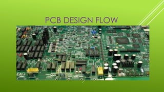
Flow of PCB Designing in the manufacturing process
- 2. The PCB Design Flow can Split into Two Fundamental Stages: 1. PROTOTYPING 2. PRODUCT DEVELOPMENT STAGE
- 3. PROTOTYPING: It occurs at the earliest stage of design and involves individual engineers researching how to define a certain system or application. the experimental nature of this stage is fundamental in being able to develop hardware that can meet specifications. when the design has been validated, it can be passed onto the latter stages of the design flow (i.e. product development). the ultimate goal of the prototyping stage is to have a successful product that is accurate, efficient and meets specifications. you want to accomplish this with as few prototype iterations as possible to maximize time and resources. PRODUCT DEVELOPMENT : It is about making a PCB ready for a final application. the prototype has already met the design specifications (filtering, amplification, acquisition, measurement etc…) and it is now ready to take that design and to implement it using the best practices in design. most companies have individuals that are layout experts, and are involved in product development. during this design stage, you are developing for manufacturing and as such are concerned about increasing product yields and decreasing manufacturing re-spins.
- 4. PROTOTYPE DESIGN FLOW For prototyping you need to be able to: Define a circuit schematic quickly You need to validate circuit behavior with advanced analysis Transfer a schematic to layout easily Validate the behavior of the design accurately
- 5. There are six main reasons to prototype: 1. Fail early and inexpensively: Real innovation always includes a risk of failure. By building a prototype, you can quickly weed out the approaches that don’t work to focus on the ones that do. 2. Gather more accurate requirements: Almost half of all project costs are attributed to rework due to inadequate requirements. By developing a working prototype, you can demonstrate the functionality to help solidify requirements for the final design. 3. Technically understand the problem: By developing a functional prototype, you can address both the foreseen and the unforeseen technical challenges of a device’s design. You can then apply those solutions to a more elegant system design when you move to the final deployed solution. Why Prototype?
- 6. 4. Resolve conflicts: By taking advantage of a prototyping platform, you can quickly conduct several different implementations of the feature and benchmark the resulting performance to analyze the trade-offs of each approach. This can save time, but it also ensures that you make the correct design decisions. 5. Financial support: By developing a prototype to demonstrate the feasibility of your idea, you lower the risk of investment and therefore increase the probability that your idea will be funded. 6. File patents more easily: Though no longer required, a prototype is still the best and safest way to demonstrate “reduction to practice.” Furthermore, key components of a patent application, such as patent drawings and the inventor’s logbook.
- 7. PCB DESIGN FLOW: PRODUCT DEVELOPMENT PART RESEARCH & SELECTION SCHEMATIC CAPTURE SIMULATION BOARD LAYOUT VERIFICATION & VALIDATION
- 8. Before even designing, needs to be able to select components that will make a circuit function. there are a number of semiconductor manufacturers including analog devices, national semiconductor, nxp,linear tech, semi and texas instruments, that create devices that meet varying specifications, there are a number of ways for designer to research parts. Step 1 - PART RESEARCH & SELECTION:
- 9. Schematic capture involves taking symbolic representations of components (resistors, capacitors, amplifiers, comparators etc…) and wiring them together into a visual diagram which can be easily viewed to understand the functionality of the circuit. The purpose of the schematic is to view the building blocks of the circuit from a theoretical perspective. Step 2 - SCHEMATIC CAPTURE In the schematic consists of component symbols and wires.
- 10. simulation is the industry standard in simulation of circuit components. simulation can be used to evaluate the behavior of real world components in a virtual environment, thereby allowing you to do advanced analysis of a design earlier in the design flow, by visualizing the behavior of the circuit at the earliest stage of prototyping, one can reduce errors and improve performance. . Step 3 - Simulation Designer often build the schematic of their design, and then simulate and visualize its characteristics.
- 11. A schematic when completed is transferred to board layout, each symbol in a schematic is associated with a land pattern. a land pattern visually represents the physical dimensions of an IC or semiconductor package. the land pattern translates the symbol of a component (such as an operational amplifier) to an 8 pin rectangular package, during the board layout stage the design is defined as it will eventually look when prototyped, this means defining the board outline, placing parts, creating connections between parts in copper, and then finally exporting for fabrication. STEP 4 - BOARD LAYOUT
- 12. Once the board is fabricated, the engineer needs to validate the behavior of the prototype. Once it is validated, it can be handed off to product development and be prepared for manufacturing. validation requires taking measurements from the board and ensuring that real performance meets the simulated performance (or specifications). STEP 5- VERIFICATION & VALIDATION
- 13. Thank You