1. Chapter 3.3 Computer Architecture and the Fetch-Execute Cycle
3.3 (a) Von Neumann Architecture
John Von Neumann introduced the idea of the stored program. Previously data and
programs were stored in separate memories. Von Neumann realised that data and
programs are indistinguishable and can, therefore, use the same memory. This led to
the introduction of compilers which accepted text as input and produced binary code
as output.
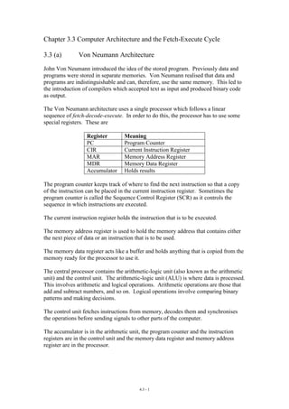
The Von Neumann architecture uses a single processor which follows a linear
sequence of fetch-decode-execute. In order to do this, the processor has to use some
special registers. These are
Register Meaning
PC Program Counter
CIR Current Instruction Register
MAR Memory Address Register
MDR Memory Data Register
Accumulator Holds results
The program counter keeps track of where to find the next instruction so that a copy
of the instruction can be placed in the current instruction register. Sometimes the
program counter is called the Sequence Control Register (SCR) as it controls the
sequence in which instructions are executed.
The current instruction register holds the instruction that is to be executed.
The memory address register is used to hold the memory address that contains either
the next piece of data or an instruction that is to be used.
The memory data register acts like a buffer and holds anything that is copied from the
memory ready for the processor to use it.
The central processor contains the arithmetic-logic unit (also known as the arithmetic
unit) and the control unit. The arithmetic-logic unit (ALU) is where data is processed.
This involves arithmetic and logical operations. Arithmetic operations are those that
add and subtract numbers, and so on. Logical operations involve comparing binary
patterns and making decisions.
The control unit fetches instructions from memory, decodes them and synchronises
the operations before sending signals to other parts of the computer.
The accumulator is in the arithmetic unit, the program counter and the instruction
registers are in the control unit and the memory data register and memory address
register are in the processor.
4.3 - 1
2. 3.3 (b) The Fetch-Decode-Execute-Reset Cycle
The following is an algorithm that shows the steps in the cycle. At the end the cycle
is reset and the algorithm repeated.
1. Load the address that is in the program counter (PC) into the memory address
register (MAR).
2. Increment the PC by 1.
3. Load the instruction that is in the memory address given by the MAR into the
memory data register (MDR).
4. Load the instruction that is now in the MDR into the current instruction
register (CIR).
5. Decode the instruction that is in the CIR.
6. If the instruction is a jump instruction then
a. Load the address part of the instruction into the PC
b. Reset by going to step 1.
7. Execute the instruction.
8. Reset by going to step 1.
Steps 1 to 4 are the fetch part of the cycle. Steps 5, 6a and 7 are the execute part of
the cycle and steps 6b and 8 are the reset part.
Step 1 simply places the address of the next instruction into the memory address
register so that the control unit can fetch the instruction from the right part of the
memory. The program counter is then incremented by 1 so that it contains the address
of the next instruction, assuming that the instructions are in consecutive locations.
The memory data register is used whenever anything is to go from the central
processing unit to main memory, or vice versa. Thus the next instruction is copied
from memory into the MDR and is then copied into the current instruction register.
Now that the instruction has been fetched the control unit can decode it and decide
what has to be done. This is the execute part of the cycle. If it is an arithmetic
instruction, this can be executed and the cycle restarted as the PC contains the address
of the next instruction in order. However, if the instruction involves jumping to an
instruction that is not the next one in order, the PC has to be loaded with the address
of the instruction that is to be executed next. This address is in the address part of the
current instruction, hence the address part is loaded into the PC before the cycle is
reset and starts all over again.
4.3 - 2
3. 3.3 (c) Parallel Processor Systems
Using the above architecture for a microprocessor illustrates that basically an
instruction can be in one of three phases. It could be being fetched (from memory),
decoded (by the control unit) or being executed (by the control unit). An alternative is
to split the processor up into three parts, each of which handles one of the three
stages. This would result in the situation shown in Fig. 3.3.c.1, which shows how this
process, known as pipelining, works.
Fetch Decode Execute
Instruction 1
Instruction 2 Instruction 1
Instruction 3 Instruction 2 Instruction 1
Instruction 4 Instruction 3 Instruction 2
Instruction 5 Instruction 4 Instruction 3
Fig. 3.3.c.1
The effect of pipe lining is that there are three instructions being dealt with at the
same time. This SHOULD reduce the execution times considerably (to approximately
1/3 of the standard times), however, this would only be true for a very linear program.
Once jump instructions are introduced the problem arises that the wrong instructions
are in the pipe line waiting to be executed, so every time the sequence of instructions
changes, the pipe line has to be cleared and the process started again.
Another type of computer architecture is to use many processors, each carrying out an
individual instruction at the same time as its partners. This type of processing
uses an architecture known as parallel processing, which involves many
independent processors working in parallel on the same program. One of the
difficulties with this is that the programs running on these systems need to
have been written specially for them. If the programs have been written for
standard architectures, then some instructions cannot be completed until
others have been completed. Thus, checks have to be made to ensure that all
prerequisites have been completed. However, these systems are in use
particularly when systems are receiving many inputs from sensors and the data
need to be processed in parallel.
4.3 - 3