
Recommandé
Contenu connexe
Tendances
Tendances (19)
Similaire à Assignment#3a
Similaire à Assignment#3a (20)
Plus de Sunita Milind Dol
Plus de Sunita Milind Dol (20)
Dernier
Dernier (20)
Assignment#3a
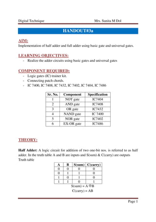
- 1. Digital Technique Mrs. Sunita M Dol Page 1 HANDOUT#3a AIM: Implementation of half adder and full adder using basic gate and universal gates. LEARNING OBJECTIVES: - Realize the adder circuits using basic gates and universal gates COMPONENT REQUIRED: - Logic gates (IC) trainer kit. - Connecting patch chords. - IC 7400, IC 7408, IC 7432, IC 7402, IC 7404, IC 7486 Sr. No. Component Specification 1 NOT gate IC7404 2 AND gate IC7408 3 OR gate IC7432 4 NAND gate IC 7400 5 NOR gate IC7402 6 EX-OR gate IC7486 THEORY: Half Adder: A logic circuit for addition of two one-bit nos. is referred to as half adder. In the truth table A and B are inputs and S(sum) & C(carry) are outputs Truth table A B S(sum) C(carry) 0 0 0 0 0 1 1 0 1 0 1 0 1 1 0 1 S(sum) = A B C(carry) = AB
- 2. Digital Technique Mrs. Sunita M Dol Page 2 Half Adder using basic gates: Using NAND gate only
- 3. Digital Technique Mrs. Sunita M Dol Page 3 Using only NOR gate
- 4. Digital Technique Mrs. Sunita M Dol Page 4 Full Adder: An half adder has only two inputs and there is no provision to add a carry coming from the lower bits when multibit addition is performed. For this purpose, a 3rd input terminal is added and this circuit is used to add An, Bn and Cn-1 where An & Bn are the nth order bit of the numbers A and B respectively and Cn-1 is the carry generated from the addition of (n-1)th order bit. This circuit is referred to as Full Adder. Truth table An Bn Cn-1 Sn(sum) Cn(carry) 0 0 0 0 0 0 0 1 1 0 0 1 0 1 0 0 1 1 0 1 1 0 0 1 0 1 0 1 0 1 1 1 0 0 1 1 1 1 1 1 Logic Equation:
- 5. Digital Technique Mrs. Sunita M Dol Page 5 Logic Circuit using Basic gates: For S(sum)
- 6. Digital Technique Mrs. Sunita M Dol Page 6 For C(Carry) For S and C using two half adder
- 7. Digital Technique Mrs. Sunita M Dol Page 7 Using NAND gate only For Sn(sum)
- 8. Digital Technique Mrs. Sunita M Dol Page 8 For Cn(carry)
- 9. Digital Technique Mrs. Sunita M Dol Page 9 Using NOR gate only For Sn(sum)
- 10. Digital Technique Mrs. Sunita M Dol Page 10 For Cn(carry) PROCEDURE: 1. Check the components for their working. 2. Insert the appropriate IC into the IC base. 3. Make connections as shown in the circuit diagram. 4. Provide the input data via the input switches and observe the output on output LEDs 5. Give various combinations of inputs and note down the output with help of LED for all gate ICs one by one. RESULT: Thus we have implemented half adder and full adder using basic gate and universal gates