Boost Converter Circuit (Step-up) using PSpice
•Télécharger en tant que PPT, PDF•
0 j'aime•326 vues

Boost Converter Circuit (Step-up)

Recommandé
Contenu connexe
Tendances
Tendances (20)
Similaire à Boost Converter Circuit (Step-up) using PSpice
Similaire à Boost Converter Circuit (Step-up) using PSpice (20)
Plus de Tsuyoshi Horigome
Plus de Tsuyoshi Horigome (20)
Dernier
Dernier (20)
Boost Converter Circuit (Step-up) using PSpice
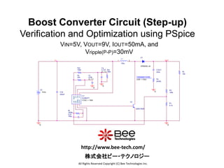
- 1. Boost Converter Circuit (Step-up) Verification and Optimization using PSpice VIN=5V, VOUT=9V, IOUT=50mA, and Vripple(P-P)=30mV L1 150u 1 2 CLP 100p Q1 Q2SC3526 Rf 1000k Rsr 180k Cs 4.7uF IC = 0 0 0 U1 NJM2377 FOSC = 150K -IN FB GND OUT V+ CS CT REF RL 180 OUT Rt 24k Ct 470p IC = 0 0 CIN 220uF V+ 0 Rsf 160k R1 9.1k R2 150k Rs {ESR} 0 D1 DRB055L-40 PARAMETERS: ESR = 103m V2 5Vdc COUT 220u All Rights Reserved Copyright (C) Bee Technologies Inc. 株式会社ビー・テクノロジー http://www.bee-tech.com/
- 2. All Rights Reserved Copyright (C) Bee Technologies Inc. Content 1.Circuit Design Verification: Design Condition: VIN=5V, VOUT=9V, IOUT=50mA, and Vripple(P-P)=30mV 2.Output Stage Optimization: COUT 220uF 2.1 ESR Characteristics Comparison 2.2 Ripple Voltage Comparison 3 Output Stage Optimization: D1 3.1 Characteristics Comparison 3.2 Diode Performance Comparison 4.Schottky Diode Reverse Characteristics RB055L-40 Standard vs. Professional Model 4.1 Comparison Result Voltage, Current, and Power of D1 in Boost Converter Circuit 5 Power Switch: Q1 5.1 Power Switch: Q1 PC, IB, VC, and IC Simulation Result 5.2 Power Switch: Q1 Power Stage Device Stress Analysis
- 3. Time 118.0ms 118.4ms 118.8ms 119.2ms 119.6ms 120.0ms -I(RL) 0A 50mA 100mA V(OUT) 9.045V 9.065V 9.075V 9.085V 9.095V SEL>> V(V+) V(OUT) 0V 2.5V 5.0V 7.5V 10.0V 1.Circuit Design Verification Design Condition: VIN=5V, VOUT=9V, IOUT=50mA, and Vripple(P-P)=30mV VIN=5V VOUT=9V Vripple(P-P)=30mV IOUT=50mA
- 4. 2.Output Stage Optimization: COUT 220uF RJJ-35V221MG5-T20 from ELNA vs. LXZ25VB220MH12 from Nippon Chemi-Con Corporation L1 150u 1 2 CLP 100p Q1 Q2SC3526 Rf 1000k Rsr 180k Cs 4.7uF IC = 0 0 0 U1 NJM2377 FOSC = 150K -IN FB GND OUT V+ CS CT REF RL 180 OUT Rt 24k Ct 470p IC = 0 0 CIN 220uF V+ 0 Rsf 160k R1 9.1k R2 150k Rs {ESR} 0 D1 DRB055L-40 PARAMETERS: ESR = 103m V2 5Vdc COUT 220u ESR
- 5. 2.1 ESR Characteristics Comparison RJJ-35V221MG5-T20 from ELNA vs. LXZ25VB220MH12 from Nippon Chemi-Con Corporation Part number ESR() (Condition: frequency=150kHz) RJJ-35V221MG5-T20 195m LXZ25VB220MH12 809m ELNA RJJ-35V221MG5-T20 Nippon Chemi-Con Corporation LXZ25VB220MH12
- 6. Time 100ms 101ms 102ms 103ms 104ms 105ms V(OUT) 8.90V 8.95V 9.00V 9.05V 9.10V 9.15V 9.20V 2.2 Ripple Voltage Comparison RJJ-35V221MG5-T20 from ELNA vs. LXZ25VB220MH12 from Nippon Chemi-Con Corporation VIN=5V Vout ripple for ESR 809m 150mV Vout ripple for ESR 195m 50mV Total job time (using Solver 1) = 1437.91 sec. (24min.)
- 7. 3.Output Stage Optimization: D1 ROHM’s Schottky Diode: RB051L-40 vs. RB055L-40 L1 150u 1 2 CLP 100p Q1 Q2SC3526 Rf 1000k Rsr 180k Cs 4.7uF IC = 0 0 0 U1 NJM2377 FOSC = 150K -IN FB GND OUT V+ CS CT REF RL 180 OUT Rt 24k Ct 470p IC = 0 0 CIN 220uF V+ 0 Rsf 160k R1 9.1k R2 150k Rs {ESR} 0 D1 DRB055L-40 PARAMETERS: ESR = 103m V2 5Vdc COUT 220u Replace Model
- 8. 3.1 Characteristics Comparison ROHM’s Schottky Diode: RB051L-40 vs. RB055L-40 Part number VF (V) (Condition: IF=100mA) Ct (pF) (Condition: VR=9V) VR (Max.) RB051L-40 0.232 213.800 40V RB055L-40 0.320 69.910 40V VF-IF characteristics Ct-VR characteristics
- 9. 3.2 Diode Performance Comparison ROHM’s Schottky Diode: RB051L-40 vs. RB055L-40 76% PD(rms) Decrease I(AK) V(KA) PD(rms) The waveforms of DRB051L-40 The waveforms of DRB055L-40
- 10. 4.Schottky Diode Reverse Characteristics RB055L-40 Standard vs. Professional Model 0.1 1 10 100 0 10 20 30 40 REVERSE CURRENT:IR(uA) REVERSE VOLTAGE:VR(V) VR-IR CHARACTERISTICS Datasheet Standard Professional Reverse characteristics
- 11. 4.1 Comparison Result Voltage, Current, and Power of D1 in Boost Converter Circuit Professional Model Time 119.980ms 119.985ms 119.990ms 119.995ms rms(V(U2:A,U2:K)*I(U2:A)) 20mW 30mW 35mW 40mW SEL>> (119.990m,28.917m) I(U2:A) -100mA 0A 100mA V(U2:A,U2:K) -10V -5V 0V Time 119.980ms 119.985ms 119.990ms 119.995ms rms(V(D1:A,D1:c)*I(D1)) 20mW 30mW 40mW SEL>> (119.990m,29.955m) I(D1) -100mA 0A 100mA V(D1:A,D1:c) -10V -5V 0V Standard Model PD(rms) = 28.917mW PD(rms) = 29.955mW V(AK) I(AK) V(AK) I(AK)
- 12. L1 150u 1 2 CLP 100p Rf 1000k Rsr 180k Cs 4.7uF IC = 0 0 0 U1 NJM2377 FOSC = 150K -IN FB GND OUT V+ CS CT REF RL 180 Q1 Q2SD2623 U2RB055L-40 OUT Rt 24k Ct 470p IC = 0 0 CIN 220uF V+ 0 Rsf 160k R1 9.1k R2 150k Rs {ESR} 0 PARAMETERS: ESR = 103m V2 5Vdc COUT 220u 5.Power Switch: Q1 Panasonic’s NPN Transistor: 2SD2623 BJT Power Switch
- 13. 5.1 Power Switch: Q1 PC, IB, VC, and IC Simulation Result IB VC IC PC
- 14. 5.2 Power Switch: Q1 Power Stage Device Stress Analysis Parameter Start-Up Steady-State Absolute Maximum Ratings VCE (V) 9.322 (46.61% of VCEO) 9.368 (46.84% of VCEO) VCEO=20V IC (A) 0.287 (57.4% of ICmax) 0.093 (18.6% of ICmax) ICmax.=0.5A