SlideShare une entreprise Scribd logo
1  sur  17
QUAID-E-AWAM UNIVERSITY OF ENGINEERING SCIENCE & TECHNOLOGY
                                      NAWABSHAH

               DEPARTMENT OF INFORMATION TECHNOLOGY

Digital Logic & Computer Architects                     (3rd Term, 2nd Year)

                                             PRACTICAL # 01

      OBJECTIVE: To Become Familiar With Basic Binary Operation.

      TOOL: Electronic Work Bench V 5.12

      EQUIPMENT AND COMPONENTS:

              Logic Gates
              Indicator (LED)
              Two Switches
              Ground
              Voltage Source


      AND Gate:

      Logic Expression:                A.B= Y


      Logic Symbol:


      Truth Table:
                                        INPUTS                  OUTPUT
                                   A               B                 Y
                                   0               0                 0
                                   0               1                 0
                                   1               0                 0
                                   1               1                 1
      Explanation:
                       The AND gate is a logic device whose output is 1 if and only if all its inputs
      are 1. In other words the output of an AND gate is 0 if any one or both its inputs are 0. It can
      have two or more inputs can only one output.
      It is also called an all or nothing gate, because it produces a 1 only in one case when all its
      inputs are a 1. In all other cases its output is zero.
QUAID-E-AWAM UNIVERSITY OF ENGINEERING SCIENCE & TECHNOLOGY
                                   NAWABSHAH

              DEPARTMENT OF INFORMATION TECHNOLOGY

Digital Logic & Computer Architects                     (3rd Term, 2nd Year)

                                             PRACTICAL # 01


      OR Gate:


      Logic Expression:                A+B= Y


      Logic Symbol:


      Truth Table:
                                        INPUTS                   OUTPUT
                                   A               B                   Y
                                   0               0                   0
                                   0               1                   1
                                   1               0                   1
                                   1               1                   1


      Explanation:
                      The OR gate is a logic device whose output is 1 if at least one if its input is 1.
      In other words the output of an OR gate is 0 if both its inputs are 0.
      It is also called any or all gate, because it produces a 1 even if one of its inputs is at 1.
      It produces a 0 only when all the inputs are 0.
Viva Question:

Q: 1 why we use logic Gates?
Ans: Logic gates are used to make logic circuits.


Q: 2 Advantages of logic gates?
Ans: Logic gates are basic components of microprocessors. Without them, electronics
systems couldn't run.


Q: 3 what is also called NOT gate?
Ans: The NOT gate also called INVERTER.


Q: 4 Where output of AND Gate is high and low?
Ans: If both inputs are high the output will be high/true/on else output of AND gate is
low/false/off.
QUAID-E-AWAM UNIVERSITY OF ENGINEERING SCIENCE & TECHNOLOGY
                                     NAWABSHAH

              DEPARTMENT OF INFORMATION TECHNOLOGY

Digital Logic & Computer Architects                  (3rd Term, 2nd Year)

                                          PRACTICAL # 02

      OBJECTIVE: To implement and verify the NOR gate, NAND gate operations.

      TOOL: Electronic Work Bench V 5.12

      EQUIPMENT AND COMPONENTS:

             Logic Gates
             Indicator (LED)
             Two Switches
             Ground
             Voltage Source


      NOR Gate:

      Logic Expression:              ( A + B)¯ = Y


      Logic Symbol:


      Truth Table:
                                      INPUTS                  OUTPUT
                                 A              B                   Y
                                 0              0                   1
                                 0              1                   0
                                 1              0                   0
                                 1              1                   0


      Explanation:


                     The NOR gate is a device whose out is 1 if and only if all inputs are at 0. In all
      other cases the output is 0. The name NOR is derived from NOT-OR, because the gate
      performs the same logic as OR gate followed by an inverter. It is a universal gate. It can also
      be used as an inverter.
QUAID-E-AWAM UNIVERSITY OF ENGINEERING SCIENCE & TECHNOLOGY
                                                   NAWABSHAH


              DEPARTMENT OF INFORMATION TECHNOLOGY

Digital Logic & Computer Architects                    (3rd Term, 2nd Year)


                                         PRACTICAL # 02

      NAND Gate:

      Logic Expression:               ( A . B)¯ = Y


      Logic Symbol:


      Truth Table:
                                       INPUTS                  OUTPUT
                                  A              B                   Y
                                  0              0                   1
                                  0              1                   1
                                  1              0                   1
                                  1              1                   0


      Explanation:
                     The NAND gate is a device whose output is 1 if at least one of its inputs is 0.
      Thus the output is 0 when all its inputs are 1. The name NAND is derived from NOT-AND
      because the gate performs the same logic as AND gate followed by an inverter. It is a
      universal gate as all basic gates can be derived from it. It can also be used as an inverter.
                                          VIVA QUESTIONS
      Q: 1 NOR gate is combination of?
      Ans: NOR gate is the combination of OR gate and NOT gate.

      Q: 2 NAND gate is combination of?
      sAns: NAND gate is combination of AND gate and NOT gate.

      Q: 3 Where output of NOR gate is high and low?
      Ans: If any one or both input is high the output will be low else output will high.


      Q: 4 where output of NAND gate is high and low?
      Ans: If both input high the output will be low else output will high.
QUAID-E-AWAM UNIVERSITY OF ENGINEERING SCIENCE & TECHNOLOGY
                                                 NAWABSHAH


             DEPARTMENT OF INFORMATION TECHNOLOGY

Digital Logic & Computer Architects                 (3rd Term, 2nd Year)


                                       PRACTICAL # 03
      OBJECTIVE: To understand the operation of EX-OR & EX-NOR gates.

      TOOL: Electronic Work Bench V 5.12

      EQUIPMENT AND COMPONENTS:

            Logic Gates
            Indicator (LED)
            Two Switches
            Ground
            Voltage Source


      EX-OR Gate:


      Logic Expression:              F = x‟y + xy‟


      Logic Symbol:


      Truth Table:
                                     INPUTS                  OUTPUT
                                 X             Y                  F
                                 0             0                  0
                                 0             1                  1
                                 1             0                  1
                                 1             1                  0


      Explanation:
             If inputs are similar output of X-OR gate will be “low” (0).
             If inputs are dissimilar or change than output of X-OR gate will be “High” (1).
EX-NOR Gate:


Logic Expression:              F = x‟ y „ . x y


Logic Symbol:


Truth Table:
                                INPUTS                 OUTPUT
                           X             Y                  F
                           0             0                  1
                           0             1                  0
                           1             0                  0
                           1             1                  1


Explanation:
       If inputs are similar output of X-NOR gate will be “High” (1).
       If inputs are dissimilar or change than output of X-OR gate will be “Low” (0).


                                      Viva Question:

Q.01: What is operation of EX-OR gate?

ANS: If inputs are similar output of EX-OR gate will be low. If inputs are dissimilar or
change than output of EX-OR gate will be high.


Q.02: What is operation of EX-NOR gate?

ANS: If inputs are similar output of EX-NOR gate will be high. If inputs are dissimilar or
change than output of EX-NOR gate will be low.
QUAID-E-AWAM UNIVERSITY OF ENGINEERING SCIENCE & TECHNOLOGY
                                              NAWABSHAH


             DEPARTMENT OF INFORMATION TECHNOLOGY

Digital Logic & Computer Architects              (3rd Term, 2nd Year)


                                      PRACTICAL # 04
      OBJECTIVE: To Design the circuit of the Boolean expression & verify the result through
                 truth table.

      TOOL: Electronic Work Bench V 5.12

      EQUIPMENT AND COMPONENTS:

            Logic Gates
            Indicator (LED)
            Two Switches
            Ground
            Voltage Source


         1. F= (a.b) (b`+c)


      Truth Table:                               S.No     A      B      C   F
                                                   0      0      0      0   0
                                                   1      0      0      1   0
                                                   2      0      1      0   0
                                                   3      0      1      1   0
                                                   4      1      0      0   0
                                                   5      1      0      1   0
                                                   6      1      1      0   0
                                                   7      1      1      1   1
2. F= (a`+b`) (c`+d) (d+c)


Truth Table:
                             S:NO   A   B   C   D   F
                              0     0   0   0   0   0
                              1     0   0   0   1   1
                              2     0   0   1   0   0
                              3     0   0   1   1   1
                              4     0   1   0   0   0
                              5     0   1   0   1   1
                              6     0   1   1   0   0
                              7     0   1   1   1   1
                              8     1   0   0   0   0
                              9     1   0   0   1   1
                             10     1   0   1   0   0
                             11     1   0   1   1   1
                             12     1   1   0   0   0
                             13     1   1   0   1   0
                             14     1   1   1   0   0
                             15     1   1   1   1   0
3. F= {(x`+y) `+(x+y) `+(y+z`)}


Truth Table:

                                  S:NO   X   Y   Z   F
                                   0     0   0   0   1
                                   1     0   0   1   1
                                   2     0   1   0   0
                                   3     0   1   1   1
                                   4     1   0   0   0
                                   5     1   0   1   0
                                   6     1   1   0   1
                                   7     1   1   1   1
4. F= [(a+b+c) `] [(d`e)]


Truth Table:


                            S:NO   A   B   C   D   E   F
                             0     0   0   0   0   0   0
                             1     0   0   0   0   1   0
                             2     0   0   0   1   0   0
                             3     0   0   0   1   1   0
                             4     0   0   1   0   0   0
                             5     0   0   1   0   1   1
                             6     0   0   1   1   0   0
                             7     0   0   1   1   1   0
                             8     0   1   0   0   0   0
                             9     0   1   0   0   1   1
                            10     0   1   0   1   0   0
                            11     0   1   0   1   1   0
                            12     0   1   1   0   0   0
                            13     0   1   1   0   1   1
                            14     0   1   1   1   0   0
                            15     0   1   1   1   1   0
QUAID-E-AWAM UNIVERSITY OF ENGINEERING SCIENCE & TECHNOLOGY
                                                   NAWABSHAH


              DEPARTMENT OF INFORMATION TECHNOLOGY

Digital Logic & Computer Architects                   (3rd Term, 2nd Year)


                                         PRACTICAL # 05
      OBJECTIVE: To observe the operation of logic converter.

      TOOL: Electronic Work Bench V 5.12

      EQUIPMENT AND COMPONENTS:

            Logic Gates
            Indicator (LED)
            Two Switches
            Ground
            Voltage Source

      THEORY:

       The logic converter is able to perform several transformations of a circuit representation. It
      has no real-world counterpart. It can be attached to a circuit to derive the truth table or
      Boolean expression the circuit embodies, or used to produce a circuit from a truth table or
      Boolean expression.


      PROCEDURE:

               1.   First we open the electronic workbench.
               2.   Get an OR gate.
               3.   Two NOT gates and tow AND gates from logic gates and one converter.
               4.   Connect inputs to left side of converter and output to the right side of the
                    converter.
TO CONSTRUCT A TRUTH TABLE:

1.       Click the number of input channels you want, from a to H, across the top of the logic
converter. The display area below the terminals fills up with the necessary combinations of
ones and zeros to fulfill the input conditions. The values in the output column on the right are
initially set to 0.
2.       Edit the output column to specify the desired output for each input condition.
To change an output value, select it and type a new value: 1, 0 or x. (An x indicates that
either 1 or 0 is acceptable.)
         To convert a truth table to a Boolean expression, click the Truth Table to Boolean
Expression button.
The Boolean expression will be displayed at the bottom of the logic converter.
To convert a truth table to a simplified Boolean expression, or to simplify an existing
Boolean expression, click the Simplify button which is shown in the figure.


RESULT:

                      The result is observed by the logic converters.
QUAID-E-AWAM UNIVERSITY OF ENGINEERING SCIENCE & TECHNOLOGY
                                                 NAWABSHAH


             DEPARTMENT OF INFORMATION TECHNOLOGY

Digital Logic & Computer Architects                 (3rd Term, 2nd Year)


                                       PRACTICAL # 06
      OBJECTIVE:          Task 1: Design full adder circuit.

                          Task 2: Design a BCD to Excess-3 code converter.

      TOOL: Electronic Work Bench V 5.12

      EQUIPMENT AND COMPONENTS:

            Logic Gates
            Indicator (LED)
            Two Switches
            Ground
            Voltage Source

      THEORY:

             FULL ADDER:

             A full adder is a combinational circuit that performs an arithmetic sum of three input
             bits and produces two outputs.
BCD TO EX-3:

The BCD to Ex-3 code uses four bit to represent a decimal digits there must be four input
Variable.
QUAID-E-AWAM UNIVERSITY OF ENGINEERING SCIENCE & TECHNOLOGY
                                               NAWABSHAH


             DEPARTMENT OF INFORMATION TECHNOLOGY

Digital Logic & Computer Architects                (3rd Term, 2nd Year)


                                      PRACTICAL # 07
      OBJECTIVE:          Design a combinational circuit the multiply two numbers of two bit each

      TOOL: Electronic Work Bench V 5.12

      EQUIPMENT AND COMPONENTS:

            Logic Gates
            Indicator (LED)
            Two Switches
            Ground
            Voltage Source
TRUTH TABLE:

  a1     a0    b1   b0   w   x   y   z
   0      0     0   0    0   0   0   0
   0      0     0   1    0   0   0   0
   0      0     1   0    0   0   0   0
   0      0     1   1    0   0   0   0
   0      1     0   0    0   0   0   0
   0      1     0   1    0   0   0   1
   0      1     1   0    0   0   1   0
   0      1     1   1    0   0   1   1
   1      0     0   0    0   0   0   0
   1      0     0   1    0   0   1   0
   1      0     1   0    0   1   0   0
   1      0     1   1    0   1   1   0
   1      1     0   0    0   0   0   0
   1      1     0   1    0   0   1   1
   1      1     1   0    0   1   1   0
   1      1     1   1    1   0   0   1

Contenu connexe

Tendances

Logic families ppt eceb srp
Logic families ppt eceb srpLogic families ppt eceb srp
Logic families ppt eceb srpSaikat Dutt
 
basic logic gates
 basic logic gates basic logic gates
basic logic gatesvishal gupta
 
8051 Microcontroller
8051 Microcontroller8051 Microcontroller
8051 MicrocontrollerJai Sudhan
 
Experiment write-vhdl-code-for-realize-all-logic-gates
Experiment write-vhdl-code-for-realize-all-logic-gatesExperiment write-vhdl-code-for-realize-all-logic-gates
Experiment write-vhdl-code-for-realize-all-logic-gatesRicardo Castro
 
Combinational Circuits & Sequential Circuits
Combinational Circuits & Sequential CircuitsCombinational Circuits & Sequential Circuits
Combinational Circuits & Sequential Circuitsgourav kottawar
 
Multiplexers and Demultiplexers
Multiplexers and DemultiplexersMultiplexers and Demultiplexers
Multiplexers and DemultiplexersGargiKhanna1
 
Logic gates and NAND and NOR univarsal gates
Logic gates and NAND and NOR univarsal gatesLogic gates and NAND and NOR univarsal gates
Logic gates and NAND and NOR univarsal gatesDhwanil Champaneria
 
2.3 sequantial logic circuit
2.3 sequantial logic circuit2.3 sequantial logic circuit
2.3 sequantial logic circuitWan Afirah
 
Logic Gates Presentation
Logic Gates PresentationLogic Gates Presentation
Logic Gates Presentationnad407
 
Input and output in C++
Input and output in C++Input and output in C++
Input and output in C++Nilesh Dalvi
 
slide_logic_family_pune_SE_comp
slide_logic_family_pune_SE_compslide_logic_family_pune_SE_comp
slide_logic_family_pune_SE_comphello_priti
 
Instruction set of 8086
Instruction set of 8086Instruction set of 8086
Instruction set of 8086Akhila Rahul
 
Latches and flip flop
Latches and flip flopLatches and flip flop
Latches and flip flopShuaib Hotak
 

Tendances (20)

Logic families ppt eceb srp
Logic families ppt eceb srpLogic families ppt eceb srp
Logic families ppt eceb srp
 
Deld lab manual
Deld lab manualDeld lab manual
Deld lab manual
 
basic logic gates
 basic logic gates basic logic gates
basic logic gates
 
8051 Microcontroller
8051 Microcontroller8051 Microcontroller
8051 Microcontroller
 
Verilog hdl
Verilog hdlVerilog hdl
Verilog hdl
 
Logic gates
Logic gatesLogic gates
Logic gates
 
Logic gates
Logic gatesLogic gates
Logic gates
 
Basics of Vhdl
Basics of VhdlBasics of Vhdl
Basics of Vhdl
 
Experiment write-vhdl-code-for-realize-all-logic-gates
Experiment write-vhdl-code-for-realize-all-logic-gatesExperiment write-vhdl-code-for-realize-all-logic-gates
Experiment write-vhdl-code-for-realize-all-logic-gates
 
Combinational Circuits & Sequential Circuits
Combinational Circuits & Sequential CircuitsCombinational Circuits & Sequential Circuits
Combinational Circuits & Sequential Circuits
 
Multiplexers and Demultiplexers
Multiplexers and DemultiplexersMultiplexers and Demultiplexers
Multiplexers and Demultiplexers
 
Logic gates and NAND and NOR univarsal gates
Logic gates and NAND and NOR univarsal gatesLogic gates and NAND and NOR univarsal gates
Logic gates and NAND and NOR univarsal gates
 
2.3 sequantial logic circuit
2.3 sequantial logic circuit2.3 sequantial logic circuit
2.3 sequantial logic circuit
 
Logic Gates Presentation
Logic Gates PresentationLogic Gates Presentation
Logic Gates Presentation
 
Logic gates
Logic gatesLogic gates
Logic gates
 
Input and output in C++
Input and output in C++Input and output in C++
Input and output in C++
 
slide_logic_family_pune_SE_comp
slide_logic_family_pune_SE_compslide_logic_family_pune_SE_comp
slide_logic_family_pune_SE_comp
 
Basic Logic gates
Basic Logic gatesBasic Logic gates
Basic Logic gates
 
Instruction set of 8086
Instruction set of 8086Instruction set of 8086
Instruction set of 8086
 
Latches and flip flop
Latches and flip flopLatches and flip flop
Latches and flip flop
 

En vedette

Computer workshop lecture 1 by Mohsin Rajpoot
Computer workshop lecture 1 by Mohsin RajpootComputer workshop lecture 1 by Mohsin Rajpoot
Computer workshop lecture 1 by Mohsin Rajpootmohsinraju555
 
Computer lab workshop
Computer lab workshopComputer lab workshop
Computer lab workshopMr.Ateach
 
Computer Access Workshop 23/11/11
Computer Access Workshop 23/11/11Computer Access Workshop 23/11/11
Computer Access Workshop 23/11/11Keytools
 
Digital logic design lab1
Digital logic design lab1Digital logic design lab1
Digital logic design lab1Shakeel Akram
 
Sonex Sanitary And Others Pakistan
Sonex Sanitary And Others PakistanSonex Sanitary And Others Pakistan
Sonex Sanitary And Others PakistanEmad Butt
 
computer architecture lab manual
computer architecture lab manualcomputer architecture lab manual
computer architecture lab manualNeelamani Samal
 
Workshop practice lab 1
Workshop practice lab 1Workshop practice lab 1
Workshop practice lab 1Shakeel Akram
 
digital signal-processing-lab-manual
digital signal-processing-lab-manualdigital signal-processing-lab-manual
digital signal-processing-lab-manualAhmed Alshomi
 
Lab 1 Introduction to Computer
Lab 1   Introduction to ComputerLab 1   Introduction to Computer
Lab 1 Introduction to ComputerHalimaton Sa'adiah
 
REMOTE GSM BASED MOBILE STARTER FOR MOTOR / PUMP
REMOTE GSM BASED MOBILE STARTER FOR MOTOR / PUMPREMOTE GSM BASED MOBILE STARTER FOR MOTOR / PUMP
REMOTE GSM BASED MOBILE STARTER FOR MOTOR / PUMPKHYATEE ELECTRONICS PVT.LTD
 
12th CBSE Practical File
12th CBSE Practical File12th CBSE Practical File
12th CBSE Practical FileAshwin Francis
 
EWB practical workbook
EWB practical  workbookEWB practical  workbook
EWB practical workbookserjani
 
How to Make Awesome SlideShares: Tips & Tricks
How to Make Awesome SlideShares: Tips & TricksHow to Make Awesome SlideShares: Tips & Tricks
How to Make Awesome SlideShares: Tips & TricksSlideShare
 
Getting Started With SlideShare
Getting Started With SlideShareGetting Started With SlideShare
Getting Started With SlideShareSlideShare
 

En vedette (20)

Logic converter
Logic converterLogic converter
Logic converter
 
Computer workshop lecture 1 by Mohsin Rajpoot
Computer workshop lecture 1 by Mohsin RajpootComputer workshop lecture 1 by Mohsin Rajpoot
Computer workshop lecture 1 by Mohsin Rajpoot
 
Computer lab workshop
Computer lab workshopComputer lab workshop
Computer lab workshop
 
Computer Access Workshop 23/11/11
Computer Access Workshop 23/11/11Computer Access Workshop 23/11/11
Computer Access Workshop 23/11/11
 
Digital logic design lab1
Digital logic design lab1Digital logic design lab1
Digital logic design lab1
 
Sonex Sanitary And Others Pakistan
Sonex Sanitary And Others PakistanSonex Sanitary And Others Pakistan
Sonex Sanitary And Others Pakistan
 
computer architecture lab manual
computer architecture lab manualcomputer architecture lab manual
computer architecture lab manual
 
Workshop practice lab 1
Workshop practice lab 1Workshop practice lab 1
Workshop practice lab 1
 
Cn lab manual 150702
Cn lab manual 150702Cn lab manual 150702
Cn lab manual 150702
 
Workshop practice ii lecture notes
Workshop practice ii lecture notesWorkshop practice ii lecture notes
Workshop practice ii lecture notes
 
digital signal-processing-lab-manual
digital signal-processing-lab-manualdigital signal-processing-lab-manual
digital signal-processing-lab-manual
 
Comp 107 cep ii
Comp 107 cep iiComp 107 cep ii
Comp 107 cep ii
 
Lab 1 Introduction to Computer
Lab 1   Introduction to ComputerLab 1   Introduction to Computer
Lab 1 Introduction to Computer
 
Computer Fundamental
Computer FundamentalComputer Fundamental
Computer Fundamental
 
REMOTE GSM BASED MOBILE STARTER FOR MOTOR / PUMP
REMOTE GSM BASED MOBILE STARTER FOR MOTOR / PUMPREMOTE GSM BASED MOBILE STARTER FOR MOTOR / PUMP
REMOTE GSM BASED MOBILE STARTER FOR MOTOR / PUMP
 
12th CBSE Practical File
12th CBSE Practical File12th CBSE Practical File
12th CBSE Practical File
 
Workshop practise
Workshop practiseWorkshop practise
Workshop practise
 
EWB practical workbook
EWB practical  workbookEWB practical  workbook
EWB practical workbook
 
How to Make Awesome SlideShares: Tips & Tricks
How to Make Awesome SlideShares: Tips & TricksHow to Make Awesome SlideShares: Tips & Tricks
How to Make Awesome SlideShares: Tips & Tricks
 
Getting Started With SlideShare
Getting Started With SlideShareGetting Started With SlideShare
Getting Started With SlideShare
 

Similaire à Logic Gates Fundamentals

Similaire à Logic Gates Fundamentals (20)

Report on-the-logic-gates
Report on-the-logic-gatesReport on-the-logic-gates
Report on-the-logic-gates
 
Logic gates
Logic gatesLogic gates
Logic gates
 
DOC-20240203-WA0000.pptx
DOC-20240203-WA0000.pptxDOC-20240203-WA0000.pptx
DOC-20240203-WA0000.pptx
 
Digital logic
Digital logicDigital logic
Digital logic
 
Digital logic gates and Boolean algebra
Digital logic gates and Boolean algebraDigital logic gates and Boolean algebra
Digital logic gates and Boolean algebra
 
Logic gates 07 11-2014
Logic gates 07 11-2014Logic gates 07 11-2014
Logic gates 07 11-2014
 
Lecture 04-Digital logic gates.pptx
Lecture 04-Digital logic gates.pptxLecture 04-Digital logic gates.pptx
Lecture 04-Digital logic gates.pptx
 
Class 12th Logic Gates
Class 12th Logic GatesClass 12th Logic Gates
Class 12th Logic Gates
 
Ee2 chapter3 basic_logicgates
Ee2 chapter3 basic_logicgatesEe2 chapter3 basic_logicgates
Ee2 chapter3 basic_logicgates
 
assignment_mathematics.pptx
assignment_mathematics.pptxassignment_mathematics.pptx
assignment_mathematics.pptx
 
ICT Basic Logic Gates Lessons.pptx
ICT Basic Logic Gates Lessons.pptxICT Basic Logic Gates Lessons.pptx
ICT Basic Logic Gates Lessons.pptx
 
Logic gates
Logic gatesLogic gates
Logic gates
 
Presentation On Logic Gate
Presentation On Logic Gate Presentation On Logic Gate
Presentation On Logic Gate
 
Bca i sem de lab
Bca i sem  de labBca i sem  de lab
Bca i sem de lab
 
Semiconductor Devices Class 12 Part-4
Semiconductor Devices Class 12 Part-4Semiconductor Devices Class 12 Part-4
Semiconductor Devices Class 12 Part-4
 
Physic investigatory
Physic investigatoryPhysic investigatory
Physic investigatory
 
physics investigatory on logic gates
physics investigatory on logic gatesphysics investigatory on logic gates
physics investigatory on logic gates
 
logic gates
logic gateslogic gates
logic gates
 
solids_and_semiconductor_devices_4.ppt
solids_and_semiconductor_devices_4.pptsolids_and_semiconductor_devices_4.ppt
solids_and_semiconductor_devices_4.ppt
 
Solids_And_Semiconductor_Devices_4.ppt
Solids_And_Semiconductor_Devices_4.pptSolids_And_Semiconductor_Devices_4.ppt
Solids_And_Semiconductor_Devices_4.ppt
 

Plus de Yasir Khan (20)

Lecture 6
Lecture 6Lecture 6
Lecture 6
 
Lecture 4
Lecture 4Lecture 4
Lecture 4
 
Lecture 3
Lecture 3Lecture 3
Lecture 3
 
Lecture 2
Lecture 2Lecture 2
Lecture 2
 
Lec#1
Lec#1Lec#1
Lec#1
 
Ch10 (1)
Ch10 (1)Ch10 (1)
Ch10 (1)
 
Ch09
Ch09Ch09
Ch09
 
Ch05
Ch05Ch05
Ch05
 
Snooping protocols 3
Snooping protocols 3Snooping protocols 3
Snooping protocols 3
 
Snooping 2
Snooping 2Snooping 2
Snooping 2
 
Introduction 1
Introduction 1Introduction 1
Introduction 1
 
Hpc sys
Hpc sysHpc sys
Hpc sys
 
Hpc 6 7
Hpc 6 7Hpc 6 7
Hpc 6 7
 
Hpc 4 5
Hpc 4 5Hpc 4 5
Hpc 4 5
 
Hpc 3
Hpc 3Hpc 3
Hpc 3
 
Hpc 2
Hpc 2Hpc 2
Hpc 2
 
Hpc 1
Hpc 1Hpc 1
Hpc 1
 
Flynns classification
Flynns classificationFlynns classification
Flynns classification
 
Dir based imp_5
Dir based imp_5Dir based imp_5
Dir based imp_5
 
Natural Language Processing
Natural Language ProcessingNatural Language Processing
Natural Language Processing
 

Dernier

Gas measurement O2,Co2,& ph) 04/2024.pptx
Gas measurement O2,Co2,& ph) 04/2024.pptxGas measurement O2,Co2,& ph) 04/2024.pptx
Gas measurement O2,Co2,& ph) 04/2024.pptxDr.Ibrahim Hassaan
 
MULTIDISCIPLINRY NATURE OF THE ENVIRONMENTAL STUDIES.pptx
MULTIDISCIPLINRY NATURE OF THE ENVIRONMENTAL STUDIES.pptxMULTIDISCIPLINRY NATURE OF THE ENVIRONMENTAL STUDIES.pptx
MULTIDISCIPLINRY NATURE OF THE ENVIRONMENTAL STUDIES.pptxAnupkumar Sharma
 
ACC 2024 Chronicles. Cardiology. Exam.pdf
ACC 2024 Chronicles. Cardiology. Exam.pdfACC 2024 Chronicles. Cardiology. Exam.pdf
ACC 2024 Chronicles. Cardiology. Exam.pdfSpandanaRallapalli
 
INTRODUCTION TO CATHOLIC CHRISTOLOGY.pptx
INTRODUCTION TO CATHOLIC CHRISTOLOGY.pptxINTRODUCTION TO CATHOLIC CHRISTOLOGY.pptx
INTRODUCTION TO CATHOLIC CHRISTOLOGY.pptxHumphrey A Beña
 
Inclusivity Essentials_ Creating Accessible Websites for Nonprofits .pdf
Inclusivity Essentials_ Creating Accessible Websites for Nonprofits .pdfInclusivity Essentials_ Creating Accessible Websites for Nonprofits .pdf
Inclusivity Essentials_ Creating Accessible Websites for Nonprofits .pdfTechSoup
 
Influencing policy (training slides from Fast Track Impact)
Influencing policy (training slides from Fast Track Impact)Influencing policy (training slides from Fast Track Impact)
Influencing policy (training slides from Fast Track Impact)Mark Reed
 
AMERICAN LANGUAGE HUB_Level2_Student'sBook_Answerkey.pdf
AMERICAN LANGUAGE HUB_Level2_Student'sBook_Answerkey.pdfAMERICAN LANGUAGE HUB_Level2_Student'sBook_Answerkey.pdf
AMERICAN LANGUAGE HUB_Level2_Student'sBook_Answerkey.pdfphamnguyenenglishnb
 
Full Stack Web Development Course for Beginners
Full Stack Web Development Course  for BeginnersFull Stack Web Development Course  for Beginners
Full Stack Web Development Course for BeginnersSabitha Banu
 
How to do quick user assign in kanban in Odoo 17 ERP
How to do quick user assign in kanban in Odoo 17 ERPHow to do quick user assign in kanban in Odoo 17 ERP
How to do quick user assign in kanban in Odoo 17 ERPCeline George
 
HỌC TỐT TIẾNG ANH 11 THEO CHƯƠNG TRÌNH GLOBAL SUCCESS ĐÁP ÁN CHI TIẾT - CẢ NĂ...
HỌC TỐT TIẾNG ANH 11 THEO CHƯƠNG TRÌNH GLOBAL SUCCESS ĐÁP ÁN CHI TIẾT - CẢ NĂ...HỌC TỐT TIẾNG ANH 11 THEO CHƯƠNG TRÌNH GLOBAL SUCCESS ĐÁP ÁN CHI TIẾT - CẢ NĂ...
HỌC TỐT TIẾNG ANH 11 THEO CHƯƠNG TRÌNH GLOBAL SUCCESS ĐÁP ÁN CHI TIẾT - CẢ NĂ...Nguyen Thanh Tu Collection
 
GRADE 4 - SUMMATIVE TEST QUARTER 4 ALL SUBJECTS
GRADE 4 - SUMMATIVE TEST QUARTER 4 ALL SUBJECTSGRADE 4 - SUMMATIVE TEST QUARTER 4 ALL SUBJECTS
GRADE 4 - SUMMATIVE TEST QUARTER 4 ALL SUBJECTSJoshuaGantuangco2
 
ENGLISH 7_Q4_LESSON 2_ Employing a Variety of Strategies for Effective Interp...
ENGLISH 7_Q4_LESSON 2_ Employing a Variety of Strategies for Effective Interp...ENGLISH 7_Q4_LESSON 2_ Employing a Variety of Strategies for Effective Interp...
ENGLISH 7_Q4_LESSON 2_ Employing a Variety of Strategies for Effective Interp...JhezDiaz1
 
Judging the Relevance and worth of ideas part 2.pptx
Judging the Relevance  and worth of ideas part 2.pptxJudging the Relevance  and worth of ideas part 2.pptx
Judging the Relevance and worth of ideas part 2.pptxSherlyMaeNeri
 
Choosing the Right CBSE School A Comprehensive Guide for Parents
Choosing the Right CBSE School A Comprehensive Guide for ParentsChoosing the Right CBSE School A Comprehensive Guide for Parents
Choosing the Right CBSE School A Comprehensive Guide for Parentsnavabharathschool99
 
Keynote by Prof. Wurzer at Nordex about IP-design
Keynote by Prof. Wurzer at Nordex about IP-designKeynote by Prof. Wurzer at Nordex about IP-design
Keynote by Prof. Wurzer at Nordex about IP-designMIPLM
 

Dernier (20)

Gas measurement O2,Co2,& ph) 04/2024.pptx
Gas measurement O2,Co2,& ph) 04/2024.pptxGas measurement O2,Co2,& ph) 04/2024.pptx
Gas measurement O2,Co2,& ph) 04/2024.pptx
 
MULTIDISCIPLINRY NATURE OF THE ENVIRONMENTAL STUDIES.pptx
MULTIDISCIPLINRY NATURE OF THE ENVIRONMENTAL STUDIES.pptxMULTIDISCIPLINRY NATURE OF THE ENVIRONMENTAL STUDIES.pptx
MULTIDISCIPLINRY NATURE OF THE ENVIRONMENTAL STUDIES.pptx
 
ACC 2024 Chronicles. Cardiology. Exam.pdf
ACC 2024 Chronicles. Cardiology. Exam.pdfACC 2024 Chronicles. Cardiology. Exam.pdf
ACC 2024 Chronicles. Cardiology. Exam.pdf
 
INTRODUCTION TO CATHOLIC CHRISTOLOGY.pptx
INTRODUCTION TO CATHOLIC CHRISTOLOGY.pptxINTRODUCTION TO CATHOLIC CHRISTOLOGY.pptx
INTRODUCTION TO CATHOLIC CHRISTOLOGY.pptx
 
Model Call Girl in Tilak Nagar Delhi reach out to us at 🔝9953056974🔝
Model Call Girl in Tilak Nagar Delhi reach out to us at 🔝9953056974🔝Model Call Girl in Tilak Nagar Delhi reach out to us at 🔝9953056974🔝
Model Call Girl in Tilak Nagar Delhi reach out to us at 🔝9953056974🔝
 
Inclusivity Essentials_ Creating Accessible Websites for Nonprofits .pdf
Inclusivity Essentials_ Creating Accessible Websites for Nonprofits .pdfInclusivity Essentials_ Creating Accessible Websites for Nonprofits .pdf
Inclusivity Essentials_ Creating Accessible Websites for Nonprofits .pdf
 
TataKelola dan KamSiber Kecerdasan Buatan v022.pdf
TataKelola dan KamSiber Kecerdasan Buatan v022.pdfTataKelola dan KamSiber Kecerdasan Buatan v022.pdf
TataKelola dan KamSiber Kecerdasan Buatan v022.pdf
 
Influencing policy (training slides from Fast Track Impact)
Influencing policy (training slides from Fast Track Impact)Influencing policy (training slides from Fast Track Impact)
Influencing policy (training slides from Fast Track Impact)
 
AMERICAN LANGUAGE HUB_Level2_Student'sBook_Answerkey.pdf
AMERICAN LANGUAGE HUB_Level2_Student'sBook_Answerkey.pdfAMERICAN LANGUAGE HUB_Level2_Student'sBook_Answerkey.pdf
AMERICAN LANGUAGE HUB_Level2_Student'sBook_Answerkey.pdf
 
Full Stack Web Development Course for Beginners
Full Stack Web Development Course  for BeginnersFull Stack Web Development Course  for Beginners
Full Stack Web Development Course for Beginners
 
YOUVE GOT EMAIL_FINALS_EL_DORADO_2024.pptx
YOUVE GOT EMAIL_FINALS_EL_DORADO_2024.pptxYOUVE GOT EMAIL_FINALS_EL_DORADO_2024.pptx
YOUVE GOT EMAIL_FINALS_EL_DORADO_2024.pptx
 
OS-operating systems- ch04 (Threads) ...
OS-operating systems- ch04 (Threads) ...OS-operating systems- ch04 (Threads) ...
OS-operating systems- ch04 (Threads) ...
 
How to do quick user assign in kanban in Odoo 17 ERP
How to do quick user assign in kanban in Odoo 17 ERPHow to do quick user assign in kanban in Odoo 17 ERP
How to do quick user assign in kanban in Odoo 17 ERP
 
HỌC TỐT TIẾNG ANH 11 THEO CHƯƠNG TRÌNH GLOBAL SUCCESS ĐÁP ÁN CHI TIẾT - CẢ NĂ...
HỌC TỐT TIẾNG ANH 11 THEO CHƯƠNG TRÌNH GLOBAL SUCCESS ĐÁP ÁN CHI TIẾT - CẢ NĂ...HỌC TỐT TIẾNG ANH 11 THEO CHƯƠNG TRÌNH GLOBAL SUCCESS ĐÁP ÁN CHI TIẾT - CẢ NĂ...
HỌC TỐT TIẾNG ANH 11 THEO CHƯƠNG TRÌNH GLOBAL SUCCESS ĐÁP ÁN CHI TIẾT - CẢ NĂ...
 
GRADE 4 - SUMMATIVE TEST QUARTER 4 ALL SUBJECTS
GRADE 4 - SUMMATIVE TEST QUARTER 4 ALL SUBJECTSGRADE 4 - SUMMATIVE TEST QUARTER 4 ALL SUBJECTS
GRADE 4 - SUMMATIVE TEST QUARTER 4 ALL SUBJECTS
 
ENGLISH 7_Q4_LESSON 2_ Employing a Variety of Strategies for Effective Interp...
ENGLISH 7_Q4_LESSON 2_ Employing a Variety of Strategies for Effective Interp...ENGLISH 7_Q4_LESSON 2_ Employing a Variety of Strategies for Effective Interp...
ENGLISH 7_Q4_LESSON 2_ Employing a Variety of Strategies for Effective Interp...
 
Judging the Relevance and worth of ideas part 2.pptx
Judging the Relevance  and worth of ideas part 2.pptxJudging the Relevance  and worth of ideas part 2.pptx
Judging the Relevance and worth of ideas part 2.pptx
 
Choosing the Right CBSE School A Comprehensive Guide for Parents
Choosing the Right CBSE School A Comprehensive Guide for ParentsChoosing the Right CBSE School A Comprehensive Guide for Parents
Choosing the Right CBSE School A Comprehensive Guide for Parents
 
Keynote by Prof. Wurzer at Nordex about IP-design
Keynote by Prof. Wurzer at Nordex about IP-designKeynote by Prof. Wurzer at Nordex about IP-design
Keynote by Prof. Wurzer at Nordex about IP-design
 
Raw materials used in Herbal Cosmetics.pptx
Raw materials used in Herbal Cosmetics.pptxRaw materials used in Herbal Cosmetics.pptx
Raw materials used in Herbal Cosmetics.pptx
 

Logic Gates Fundamentals

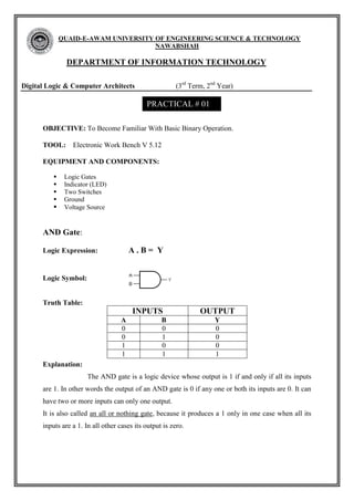
  • 1. QUAID-E-AWAM UNIVERSITY OF ENGINEERING SCIENCE & TECHNOLOGY NAWABSHAH DEPARTMENT OF INFORMATION TECHNOLOGY Digital Logic & Computer Architects (3rd Term, 2nd Year) PRACTICAL # 01 OBJECTIVE: To Become Familiar With Basic Binary Operation. TOOL: Electronic Work Bench V 5.12 EQUIPMENT AND COMPONENTS:  Logic Gates  Indicator (LED)  Two Switches  Ground  Voltage Source AND Gate: Logic Expression: A.B= Y Logic Symbol: Truth Table: INPUTS OUTPUT A B Y 0 0 0 0 1 0 1 0 0 1 1 1 Explanation: The AND gate is a logic device whose output is 1 if and only if all its inputs are 1. In other words the output of an AND gate is 0 if any one or both its inputs are 0. It can have two or more inputs can only one output. It is also called an all or nothing gate, because it produces a 1 only in one case when all its inputs are a 1. In all other cases its output is zero.
  • 2. QUAID-E-AWAM UNIVERSITY OF ENGINEERING SCIENCE & TECHNOLOGY NAWABSHAH DEPARTMENT OF INFORMATION TECHNOLOGY Digital Logic & Computer Architects (3rd Term, 2nd Year) PRACTICAL # 01 OR Gate: Logic Expression: A+B= Y Logic Symbol: Truth Table: INPUTS OUTPUT A B Y 0 0 0 0 1 1 1 0 1 1 1 1 Explanation: The OR gate is a logic device whose output is 1 if at least one if its input is 1. In other words the output of an OR gate is 0 if both its inputs are 0. It is also called any or all gate, because it produces a 1 even if one of its inputs is at 1. It produces a 0 only when all the inputs are 0.
  • 3. Viva Question: Q: 1 why we use logic Gates? Ans: Logic gates are used to make logic circuits. Q: 2 Advantages of logic gates? Ans: Logic gates are basic components of microprocessors. Without them, electronics systems couldn't run. Q: 3 what is also called NOT gate? Ans: The NOT gate also called INVERTER. Q: 4 Where output of AND Gate is high and low? Ans: If both inputs are high the output will be high/true/on else output of AND gate is low/false/off.
  • 4. QUAID-E-AWAM UNIVERSITY OF ENGINEERING SCIENCE & TECHNOLOGY NAWABSHAH DEPARTMENT OF INFORMATION TECHNOLOGY Digital Logic & Computer Architects (3rd Term, 2nd Year) PRACTICAL # 02 OBJECTIVE: To implement and verify the NOR gate, NAND gate operations. TOOL: Electronic Work Bench V 5.12 EQUIPMENT AND COMPONENTS:  Logic Gates  Indicator (LED)  Two Switches  Ground  Voltage Source NOR Gate: Logic Expression: ( A + B)¯ = Y Logic Symbol: Truth Table: INPUTS OUTPUT A B Y 0 0 1 0 1 0 1 0 0 1 1 0 Explanation: The NOR gate is a device whose out is 1 if and only if all inputs are at 0. In all other cases the output is 0. The name NOR is derived from NOT-OR, because the gate performs the same logic as OR gate followed by an inverter. It is a universal gate. It can also be used as an inverter.
  • 5. QUAID-E-AWAM UNIVERSITY OF ENGINEERING SCIENCE & TECHNOLOGY NAWABSHAH DEPARTMENT OF INFORMATION TECHNOLOGY Digital Logic & Computer Architects (3rd Term, 2nd Year) PRACTICAL # 02 NAND Gate: Logic Expression: ( A . B)¯ = Y Logic Symbol: Truth Table: INPUTS OUTPUT A B Y 0 0 1 0 1 1 1 0 1 1 1 0 Explanation: The NAND gate is a device whose output is 1 if at least one of its inputs is 0. Thus the output is 0 when all its inputs are 1. The name NAND is derived from NOT-AND because the gate performs the same logic as AND gate followed by an inverter. It is a universal gate as all basic gates can be derived from it. It can also be used as an inverter. VIVA QUESTIONS Q: 1 NOR gate is combination of? Ans: NOR gate is the combination of OR gate and NOT gate. Q: 2 NAND gate is combination of? sAns: NAND gate is combination of AND gate and NOT gate. Q: 3 Where output of NOR gate is high and low? Ans: If any one or both input is high the output will be low else output will high. Q: 4 where output of NAND gate is high and low? Ans: If both input high the output will be low else output will high.
  • 6. QUAID-E-AWAM UNIVERSITY OF ENGINEERING SCIENCE & TECHNOLOGY NAWABSHAH DEPARTMENT OF INFORMATION TECHNOLOGY Digital Logic & Computer Architects (3rd Term, 2nd Year) PRACTICAL # 03 OBJECTIVE: To understand the operation of EX-OR & EX-NOR gates. TOOL: Electronic Work Bench V 5.12 EQUIPMENT AND COMPONENTS:  Logic Gates  Indicator (LED)  Two Switches  Ground  Voltage Source EX-OR Gate: Logic Expression: F = x‟y + xy‟ Logic Symbol: Truth Table: INPUTS OUTPUT X Y F 0 0 0 0 1 1 1 0 1 1 1 0 Explanation: If inputs are similar output of X-OR gate will be “low” (0). If inputs are dissimilar or change than output of X-OR gate will be “High” (1).
  • 7. EX-NOR Gate: Logic Expression: F = x‟ y „ . x y Logic Symbol: Truth Table: INPUTS OUTPUT X Y F 0 0 1 0 1 0 1 0 0 1 1 1 Explanation: If inputs are similar output of X-NOR gate will be “High” (1). If inputs are dissimilar or change than output of X-OR gate will be “Low” (0). Viva Question: Q.01: What is operation of EX-OR gate? ANS: If inputs are similar output of EX-OR gate will be low. If inputs are dissimilar or change than output of EX-OR gate will be high. Q.02: What is operation of EX-NOR gate? ANS: If inputs are similar output of EX-NOR gate will be high. If inputs are dissimilar or change than output of EX-NOR gate will be low.
  • 8. QUAID-E-AWAM UNIVERSITY OF ENGINEERING SCIENCE & TECHNOLOGY NAWABSHAH DEPARTMENT OF INFORMATION TECHNOLOGY Digital Logic & Computer Architects (3rd Term, 2nd Year) PRACTICAL # 04 OBJECTIVE: To Design the circuit of the Boolean expression & verify the result through truth table. TOOL: Electronic Work Bench V 5.12 EQUIPMENT AND COMPONENTS:  Logic Gates  Indicator (LED)  Two Switches  Ground  Voltage Source 1. F= (a.b) (b`+c) Truth Table: S.No A B C F 0 0 0 0 0 1 0 0 1 0 2 0 1 0 0 3 0 1 1 0 4 1 0 0 0 5 1 0 1 0 6 1 1 0 0 7 1 1 1 1
  • 9. 2. F= (a`+b`) (c`+d) (d+c) Truth Table: S:NO A B C D F 0 0 0 0 0 0 1 0 0 0 1 1 2 0 0 1 0 0 3 0 0 1 1 1 4 0 1 0 0 0 5 0 1 0 1 1 6 0 1 1 0 0 7 0 1 1 1 1 8 1 0 0 0 0 9 1 0 0 1 1 10 1 0 1 0 0 11 1 0 1 1 1 12 1 1 0 0 0 13 1 1 0 1 0 14 1 1 1 0 0 15 1 1 1 1 0
  • 10. 3. F= {(x`+y) `+(x+y) `+(y+z`)} Truth Table: S:NO X Y Z F 0 0 0 0 1 1 0 0 1 1 2 0 1 0 0 3 0 1 1 1 4 1 0 0 0 5 1 0 1 0 6 1 1 0 1 7 1 1 1 1
  • 11. 4. F= [(a+b+c) `] [(d`e)] Truth Table: S:NO A B C D E F 0 0 0 0 0 0 0 1 0 0 0 0 1 0 2 0 0 0 1 0 0 3 0 0 0 1 1 0 4 0 0 1 0 0 0 5 0 0 1 0 1 1 6 0 0 1 1 0 0 7 0 0 1 1 1 0 8 0 1 0 0 0 0 9 0 1 0 0 1 1 10 0 1 0 1 0 0 11 0 1 0 1 1 0 12 0 1 1 0 0 0 13 0 1 1 0 1 1 14 0 1 1 1 0 0 15 0 1 1 1 1 0
  • 12. QUAID-E-AWAM UNIVERSITY OF ENGINEERING SCIENCE & TECHNOLOGY NAWABSHAH DEPARTMENT OF INFORMATION TECHNOLOGY Digital Logic & Computer Architects (3rd Term, 2nd Year) PRACTICAL # 05 OBJECTIVE: To observe the operation of logic converter. TOOL: Electronic Work Bench V 5.12 EQUIPMENT AND COMPONENTS:  Logic Gates  Indicator (LED)  Two Switches  Ground  Voltage Source THEORY: The logic converter is able to perform several transformations of a circuit representation. It has no real-world counterpart. It can be attached to a circuit to derive the truth table or Boolean expression the circuit embodies, or used to produce a circuit from a truth table or Boolean expression. PROCEDURE: 1. First we open the electronic workbench. 2. Get an OR gate. 3. Two NOT gates and tow AND gates from logic gates and one converter. 4. Connect inputs to left side of converter and output to the right side of the converter.
  • 13. TO CONSTRUCT A TRUTH TABLE: 1. Click the number of input channels you want, from a to H, across the top of the logic converter. The display area below the terminals fills up with the necessary combinations of ones and zeros to fulfill the input conditions. The values in the output column on the right are initially set to 0. 2. Edit the output column to specify the desired output for each input condition. To change an output value, select it and type a new value: 1, 0 or x. (An x indicates that either 1 or 0 is acceptable.) To convert a truth table to a Boolean expression, click the Truth Table to Boolean Expression button. The Boolean expression will be displayed at the bottom of the logic converter. To convert a truth table to a simplified Boolean expression, or to simplify an existing Boolean expression, click the Simplify button which is shown in the figure. RESULT:  The result is observed by the logic converters.
  • 14. QUAID-E-AWAM UNIVERSITY OF ENGINEERING SCIENCE & TECHNOLOGY NAWABSHAH DEPARTMENT OF INFORMATION TECHNOLOGY Digital Logic & Computer Architects (3rd Term, 2nd Year) PRACTICAL # 06 OBJECTIVE: Task 1: Design full adder circuit. Task 2: Design a BCD to Excess-3 code converter. TOOL: Electronic Work Bench V 5.12 EQUIPMENT AND COMPONENTS:  Logic Gates  Indicator (LED)  Two Switches  Ground  Voltage Source THEORY: FULL ADDER: A full adder is a combinational circuit that performs an arithmetic sum of three input bits and produces two outputs.
  • 15. BCD TO EX-3: The BCD to Ex-3 code uses four bit to represent a decimal digits there must be four input Variable.
  • 16. QUAID-E-AWAM UNIVERSITY OF ENGINEERING SCIENCE & TECHNOLOGY NAWABSHAH DEPARTMENT OF INFORMATION TECHNOLOGY Digital Logic & Computer Architects (3rd Term, 2nd Year) PRACTICAL # 07 OBJECTIVE: Design a combinational circuit the multiply two numbers of two bit each TOOL: Electronic Work Bench V 5.12 EQUIPMENT AND COMPONENTS:  Logic Gates  Indicator (LED)  Two Switches  Ground  Voltage Source
  • 17. TRUTH TABLE: a1 a0 b1 b0 w x y z 0 0 0 0 0 0 0 0 0 0 0 1 0 0 0 0 0 0 1 0 0 0 0 0 0 0 1 1 0 0 0 0 0 1 0 0 0 0 0 0 0 1 0 1 0 0 0 1 0 1 1 0 0 0 1 0 0 1 1 1 0 0 1 1 1 0 0 0 0 0 0 0 1 0 0 1 0 0 1 0 1 0 1 0 0 1 0 0 1 0 1 1 0 1 1 0 1 1 0 0 0 0 0 0 1 1 0 1 0 0 1 1 1 1 1 0 0 1 1 0 1 1 1 1 1 0 0 1