Nano-Imprint Technology Trends for Semiconductor Applications 2019 report by Yole Développement
•
4 j'aime•1,916 vues

Nano-Imprint Lithography is revived by photonics and biochips as well as front-end memory applications. More information on https://www.i-micronews.com/products/nano-imprint-technology-trends-for-semiconductor-applications-2019/

Recommandé
Recommandé
Contenu connexe
Tendances
Tendances (20)
Similaire à Nano-Imprint Technology Trends for Semiconductor Applications 2019 report by Yole Développement
Similaire à Nano-Imprint Technology Trends for Semiconductor Applications 2019 report by Yole Développement (20)
Plus de Yole Developpement
Plus de Yole Developpement (20)
Dernier
Dernier (20)
Nano-Imprint Technology Trends for Semiconductor Applications 2019 report by Yole Développement
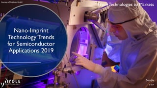
- 1. From Technologies to Markets © 2019 Nano-Imprint Technology Trends for Semiconductor Applications 2019 Sample Courtesy of: Profactor GmbH
- 2. 2 Biography & contact Nano-Imprint Technology Trends for Semiconductor Applications 2019 | Sample | www.yole.fr | ©2019 ABOUT THE AUTHOR Amandine PIZZAGALLI,Market &Technology Analyst,Equipment and Materials Manufacturing Amandine Pizzagalli oversees the equipment and materials fields for the Advanced Packaging and Manufacturing team at Yole Développement. She graduated as an engineer in Electronics, specializing in semiconductors and nanoelectronic technologies. Prior to Yole, Amandine worked for Air Liquide, with an emphasis on CVD and ALD processes for semiconductor applications. Contact: pizzagalli@yole.fr
- 3. 3 AMO,Akonia Holographics,AustriaMicrosystems, Canon, Dai Nippon Printing (DNP), Daqri, DELO, Digilens, Dispelix, EVG Group, Himax, IMS Chips, IQE, Luminit, Konica Minolta, Micro ResistTechnology, NIL Technology, Stensborg, SUSS MicroTec, MagicLeap, Microsoft, Obducat, Rockwell Collins, Sony,TOK,Toppan,Toshiba, TruLifeOptics,Trumpf, Viavi Solutions,Vuzix,WaveOptics and more… COMPANIES CITED IN THIS REPORT Nano-Imprint Technology Trends for Semiconductor Applications 2019 | Sample | www.yole.fr | ©2019
- 4. 4Nano-Imprint Technology Trends for Semiconductor Applications 2019 | Sample | www.yole.fr | ©2019 TABLE OF CONTENTS Nano-Imprint Technology Trends for Semiconductor Applications 2019 • TheThree-Pages Summary 6 • Executive Summary 10 • Introduction, Definition & Methodology 41 • Report objectives • Report scope • Who Should be interested in this report? • Companies cited in this report • Definitions, limitations & methodology • Glossary • NIL principle and technologies overview 50 • Introduction to Nano Imprint Lithography (NIL) technologies 55 • NIL definition & principle • NIL technologies classification • Consumables in the NIL process • NIL market drivers 58 • NIL technologies - benefits and drivers • SWOT analysis • NIL market segment and applications 91 • NIL at a glance • NIL applicability in the semiconductor field • NIL drivers per end application • SWOT analysis of the NIL technology per application • Competitive solutions to NIL 119 • 2018 - 2024 NIL equipment Market Forecast 129 • NIL equipment market forecast breakdown, by end-application • NIL Suppliers: Competitive Landscape 139 • NIL equipment suppliers in the field of semiconductor • NIL equipment positioning, by application • 2018 NIL equipment players’ market share and revenue In-depth analysis of NIL technologies, by end application • NIL for Optical Photonics Elements 148 • NIL for Augmented Reality (AR) 157 • Introduction to AR • Type of optical elements applied for AR • NIL functionalities • NIL benefits for AR • Benchmark of nanostructures vs alternative solutions • Players identified using NIL in AR • NIL Equipment Market forecast in wafers and in units
- 5. 5Nano-Imprint Technology Trends for Semiconductor Applications 2019 | Sample | www.yole.fr | ©2019 TABLE OF CONTENTS Nano-Imprint Technology Trends for Semiconductor Applications 2019 • NIL for 3D Sensing 172 • Introduction to 3D sensing • Type of optical elements applied for 3D sensing • NIL functionalities • NIL benefits for 3D Sensing • Benchmark of nanostructures vs alternative solutions • Players indentified using NIL in 3D Sensing • NIL Equipment Market forecast in revenue and in units • NIL for Datacom/Telecom 183 • Introduction to Data center • Type of optical elements applied for Data center/Telecommunication • NIL functionalities • NIL benefits for Data center • Benchmark of nanostructures vs alternative solutions • Players indentified using NIL in Data center • NIL Equipment Market forecast in wafers and in units • Major NIL equipment suppliers involved in Data center • NIL for BioChips 201 • Introduction to Life Science • Type of Life Science devices using NIL technology today and that could use NIL in the future • Benchmark of lithography process vs alternative solutions • Players indentified using NIL in the Life Science • Market forecast in revenue and unit • NIL for LED devices 216 • Introduction to Life Science • Type of Life Science devices using NIL technology today and that could use NIL in the future • Benchmark of lithography process vs alternative solutions • Players indentified using NIL in the Life Science • Market forecast in revenue and unit • Conclusions & Perspectives 223 • Appendix 231 • Company Presentation
- 6. 6Nano-Imprint Technology Trends for Semiconductor Applications 2019 | Sample | www.yole.fr | ©2019 OBJECTIVES OF THE REPORT This report represents the first research into NanoImprint Lithography (NIL) technologies in the semiconductor field This report aims to give an in-depth understanding of NIL technology, current status and prospects, roadblocks and key suppliers / players. Provide detailed information on which applications NIL technology could address in the semiconductor field: • Comprehensive analysis of the major applications currently using NIL methods, and potential/attractive applications that could require the use of NIL technology in the future • How disruptive NIL technology is for established and emerging applications • Discuss technology processes, specifications and value chain • NIL process applications roadmap Describe the key benefits and added-value of NIL materials in the semiconductor field: • What is NIL? What are its added values/benefits over alternative solutions? How does NIL differ from other lithography technologies? • How does NIL differ from alternative technologies? Present the current status of NIL technologies: • What are the remaining roadblocks? • Discuss the remaining challenges facing NIL technology’s implementation in the semiconductor field • Summarize current adoption status of NIL technology and the various NIL types available on the market • Provide a NIL roadmap by semiconductor application and SWOT analysis Furnish an overview of NIL’s technological trends Provide market metrics at NIL-equipment and NIL-source level for semiconductor applications (2019 - 2024) • Evaluate market developments in terms of market size (volume, value) and semiconductor process step Describe the competitive landscape and identify key players in technology development and manufacturing: • Review the key NIL equipment suppliers and position them by application, NIL type, and process step • Provide a picture of the resin, mold/stamp suppliers involved in the NIL process
- 7. 7Nano-Imprint Technology Trends for Semiconductor Applications 2019 | Sample | www.yole.fr | ©2019 METHODOLOGIES & DEFINITIONS Market Volume (in Munits) ASP (in $) Revenue (in $M) Yole’s market forecast model is based on the matching of several sources: Information Aggregation Preexisting information
- 8. 8Nano-Imprint Technology Trends for Semiconductor Applications 2019 | Sample | www.yole.fr | ©2019 LITHOGRAPHY RESOLUTION REQUIREMENTS (NON-EXHAUSTIVE LIST) Applications Devices/ Packages Patterning solution 2 µm 8 µm 20 µm 100 µm0.3 µm Stepper (DUV, EUV) Nanoimprint Advanced substrates PCB Mask aligner Stepper Projection scanner HB LED Refurbished stepper LED PSS microLED IGBT MOSFET MEMS 2.5D interposer 3D TSV FO WLP WLCSP FC BGA/FC CSPLED NPSS RF Photonic CIS Life science Point of care DNA sequencing Waveguides AR/VR Mobile Mobile WLOptics Laser direct imaging Mobile Automotive Memory and logic Report scope
- 9. 9Nano-Imprint Technology Trends for Semiconductor Applications 2019 | Sample | www.yole.fr | ©2019 NANOIMPRINT PROCESS • Nanoimprint lithography is a cost-effective fabrication technique for creating uniformly imprinted micro- and nano- scale devices in a single patterning step • NanoImprint process is a solution to transfer of patterns in the micrometer to nanometer range. Nanostructure < 1µm Microstructure >1 µm 1 µm Equipment type Feature size NanoImprint process Interference lithography Stepper NanoImprint process Hot embossing Injection Molding Mask aligner Laser direct imaging
- 10. 10Nano-Imprint Technology Trends for Semiconductor Applications 2019 | Sample | www.yole.fr | ©2019 NIL KEY MARKET DRIVERS Over alternative solutions • Three main drivers combined in NIL’s favor: • Complex patterning capabilities • High resolution manufacturing tool • Cost effective process FRONT-END STEPPER (EXTREME UV LITHOGRAPHY) MASK ALIGNER, LASER ABLATION, LASER DIRECT IMAGING COMPLEX NANOPATTERNING PROCESS HIGH RESOLUTION CAPABILITIES (<50NM) COST EFFECTIVE SOLUTION NIL optimum market access conditions * NIL : Nano-Imprint lithography
- 11. 11Nano-Imprint Technology Trends for Semiconductor Applications 2019 | Sample | www.yole.fr | ©2019 CAPITAL EQUIPMENT COMPARISON Cost Feature size capabilities 100 µm50 µm100nm 1 µm500 nm Dry Etching Wet Etching UV NIL Thermal NIL Injection molding Photolithography:Stepper Power blasting Replication technology Exposure technology Removal technology Laser ablation E-Beam Mask Aligner
- 12. 12Nano-Imprint Technology Trends for Semiconductor Applications 2019 | Sample | www.yole.fr | ©2019 MORE SLIDES EXTRACTS Understand Nano-Imprint Lithography (NIL) technologies, their drivers, main challenges as well as competitive solutions Technical description of the equipment and consumables associated with NIL technology
- 13. 13Nano-Imprint Technology Trends for Semiconductor Applications 2019 | Sample | www.yole.fr | ©2019 NIL TECHNOLOGIES - OVERVIEW • There are two fundamentals NIL technologies: Thermal NIL and UV NIL which differ from the type of resin used and the pressure conditions • The last NIL Micro Contact Printing (Soft Lithography) method is currently at the R&D phase. There are three types of NIL NILTechnologies Hot Embossing Hard Stamp Polymer Soft Stamp UV Nanoimprint Transparent Hard Stamp Polymer Soft Stamp Micro Contact Printing (Soft Lithography) Polymer Soft Stamp
- 14. 14Nano-Imprint Technology Trends for Semiconductor Applications 2019 | Sample | www.yole.fr | ©2019 Telecommunication NIL AT A GLANCE:APPLICATION MARKETS Lifescience Point-of-care Diagnostics DNA sequencing Consumer electronic devices Augmented reality 3D sensing Data center storage Optical communications Storage Organs-On-Chips BioChips Optical photonic elements Front- End Memories End-markets Elements integrated End-applications
- 15. 15Nano-Imprint Technology Trends for Semiconductor Applications 2019 | Sample | www.yole.fr | ©2019 NIL APPLICABILITY End Market End application Potential device Function Elements integrated Life Science Consumer Datacom/Telecom DNA Sequencing Point of Care (PoC) Organs-On- Chips (OOC) Source: MBEL Flow cells Diagnostic devices Nanocells Optical communication DFB laser diode Light Shaping Nanophotonic crystals Source: EVG Augmented Reality (AR) 3D Sensing Storage memory AR heads-up VCSEL 3D NAND Waveguide Beam splitter Time-Of-Flight Optical gratings (Surface Relief Gratings) Diffuser Micro-Lens-Array Nanopattern Optical gratings Storage memory (SSD) 3D NAND Nanopattern
- 16. 16Nano-Imprint Technology Trends for Semiconductor Applications 2019 | Sample | www.yole.fr | ©2019 NIL APPLICABILITY By elements integrated in end-applications Three main market segments could require the use of NIL in the semiconductor area • Microfluidic chips • Lab-on-chips • Chips with photonic structure • DNA sequencing Biochips • Optoelectronic • Optical components • DOE • Diffuser • Augmented Reality Waveguides Optical photonic elements • 3D NAND memory • DRAM Front-end memory NIL DRIVERS BiocompatibilityComplex patterningCost advantage solution
- 17. 17Nano-Imprint Technology Trends for Semiconductor Applications 2019 | Sample | www.yole.fr | ©2019 NIL ATTRIBUTESVS.APPLICATION REQUIREMENTS BioChips Photonics Front-end memory Feature size / Resolution Functionality / Compatibility Complex patterning shape Cost-effective Application Driver 1 2 4 1 3 2 31 4 4 2 31 4 2 Strong differentiator Very important Not very important or differentiating 3 Less critical
- 18. 18Nano-Imprint Technology Trends for Semiconductor Applications 2019 | Sample | www.yole.fr | ©2019 WHERE NANOIMPRINT COULD BE APPLIED? ROE DOE Nanophotonics Lens Fresnel lens Microlens Array Optical gratings SRG/Beam splitter Focusing, Collimation Microstructure (not nanostructure) Microstructure (not nanostructure) Light shaping Microstructure (not nanostructure) Pattern generator (Dot projector) Waveguide Diffuser (Flood illuminator) Use or could use nanoimprint Optical element Function type microstructure nanostructure
- 19. 19Nano-Imprint Technology Trends for Semiconductor Applications 2019 | Sample | www.yole.fr | ©2019 NIL APPLICATION ROADMAP – TIME TO MARKET Bio chips Storage memory Optical photonic elements 2018 2021 2023 2025 >2025 Point of care DNA Sequencing Organ-on-chip SRG Optical Waveguides HOE MLA for diffuser Microscale 3D NAND ?
- 20. 20Nano-Imprint Technology Trends for Semiconductor Applications 2019 | Sample | www.yole.fr | ©2019 MORE SLIDES EXTRACTS: NIL APPLICATIONS Understand in what applications NIL are used… And where NIL is emerging
- 21. 21Nano-Imprint Technology Trends for Semiconductor Applications 2019 | Sample | www.yole.fr | ©2019 2018 - 2024 NANO-IMPRINT LITHOGRAPHY EQUIPMENT MARKET SIZE Total Nano-Imprint Lithography equipment market for Semiconductor applications * BioChips Photonics elements (diffractive optical elements,refractive optical elements) 3D NAND memories – market segment developed after 2018 ~$90M CAGR +19% >$145M CAGR >20% ~$28M $10M ~$38M 2018 2024 CAGR2018-2024: >+20% >$27M ~$28M CAGR +22% *Pilot or production tools (excluding R&D tools)
- 22. 22Nano-Imprint Technology Trends for Semiconductor Applications 2019 | Sample | www.yole.fr | ©2019 Master supplier Stamp supplier Resin supplier Equipment supplier Users NIL SUPPLY CHAIN
- 23. 23Nano-Imprint Technology Trends for Semiconductor Applications 2019 | Sample | www.yole.fr | ©2019 MORE SLIDES EXTRACTS Nano-Imprint Lithography market size Nil equipment and material forecasts by market segments As well as NIL equipment market share by market
- 24. 24 Contact our SalesTeam for more information Nano-Imprint Technology Trends for Semiconductor Applications 2019 | Sample | www.yole.fr | ©2019 3D Imaging & Sensing 2018 Displays & OpticalVision Systems forVR,AR & MR 2018 Bonding and Lithography Equipment Market for More than Moore Devices Status of the Camera Module Industry 2019 – Focus on Wafer Level Optics Next Generation Sequencing & DNA Synthesis:Technology,Consumables Manufacturing and MarketTrends 2019 RELATED REPORTS Yole Développement
- 25. 25 Contact our SalesTeam for more information Nano-Imprint Technology Trends for Semiconductor Applications 2019 | Sample | www.yole.fr | ©2019 Apple iPhone X – Infrared Dot Projector RELATED REPORT System Plus Consulting
- 26. Nano-Imprint Lithography (NIL) has already been implemented for some non-semiconductor applications, mostly at the research level. Semiconductor devices mostly require photolithography technology. However, the emergence of new semiconductor devices demands tighter nanoscale resolution, complex shapes and more cost-effective lithography solutions. This has triggered the need for new patterning processes. Producers are therefore regaining interest in NIL, which is based on mechanical replication. The technology is especially relevant to photonic elements, biochips and front-end 3D NAND memory, as it enables nanoscale structures below 20 nm over large surfaces and provides complex patterning capabilities. On the photonics side, NIL technology realizes complex pattern shapes in a periodic way. For life science, the same technology ensures biocompatibility and solves the challenges of increasing complexity of biotechnology devices while enabling finer feature sizes. In the memory business, NIL could represent a cost-effective solution to achieving high-resolution feature sizes. However, there are still some big barriers that prevent NIL from entering mass production. Generally speaking, the master fabrication process appears to be a critical step that increases the Cost of Ownership (CoO) of the NIL process. Additionally, stamp lifetime and finding a trade-off between overlay, defect levels and throughput are issues that are holding back of NIL in high volume manufacturing. Solving all these limitations could be a game-changer for NIL in the semiconductor industry. This report offers a technical description of the different NIL technologies, their drivers and main challenges. NANO-IMPRINT TECHNOLOGY TRENDS FOR SEMICONDUCTOR APPLICATIONS 2019 Market & Technology Report - June 2019 Nano-Imprint Lithography is revived by photonics and biochips as well as front-end memory applications. REPORT KEY FEATURES • Detailed analysis of NIL technologies in three major semiconductor applications: photonics, biochips and front-end memories (3D NAND) • Key players and supply chain • 2018-2024 NIL equipment market forecast: breakdown by device type and end-application segment • 2018 global NIL equipment market share in the semiconductor applications • 2018 NIL equipment suppliers by device type • Overview of the players using NIL technology, by device and end- applications • Roadmap for NIL technology adoption by semiconductor device (Yole Développement, June 2019) 2018 - 2024 Nano-Imprint Lithography (NIL) equipment market size NIL’S BENEFITS COULD DISRUPT SEMICONDUCTOR APPLICATIONS Total Nano-Imprint Lithography equipment market for semiconductor applications * BioChips Photonics elements (diffractive optical elements, refractive optical elements) 3D NAND memories - Market segment developed after 2018 ~$90M CAGR +19% ~$145M CAGR 20% ~$28M $10M ~$38M 2018 2024 CAGR2018-2024 : ~20% $27M ~$28M CAGR +22% *Pilot or production tools (excluding RD tools) Excitement about NIL technologies has grown exponentially since 2014, when Canon completed its acquisition of Molecular Imprints, a start-up provider of nano-patterning systems for the hard disk drive and semiconductor sector. Numerous companies with different business models have now invested in NIL technology. They include photonic element manufacturers, epi-house foundries, microfluidic foundries or integrated device manufacturers. Their applications span augmented reality, 3D sensing and datacom/ telecommunications. This paves the way for a significant boost to NIL. Increasing demand for lower cost lithography solutions, integration of complex shapes and patterns and nanoscale structures is expected to offer many opportunities for NIL technologies. This will drive the NIL equipment market in the next few years. Although the NIL equipment business is still a niche market for semiconductor applications, it is expected to explode. Its revenue compound annual growth rate from 2018-2024 (CAGR2018- 2024) will reach an impressive 20% from, making the market worth $145M by 2024. Now the questions are: “Which semiconductor devices will revive NIL into the next-game SEMICONDUCTOR MANUFACTURING COMPLEXITY BRINGS NEW BUSINESS OPPORTUNITIES IN THE NIL EQUIPMENT MARKET
- 27. NANO-IMPRINT TECHNOLOGY TRENDS FOR SEMICONDUCTOR APPLICATIONS 2019 Nano-Imprint Lithography (NIL) technology: key market drivers (Yole Développement, June 2019) changer?” and “For which applications will NIL be used?” Currently, the real boost for the NIL equipment market is expected in photonic elements, driven by Augmented Reality (AR), 3D sensing as well as datacom/telecommunication. NIL offers the ability to imprint diffractive optical elements (DOEs) in the nanoscale. This includes optical gratings and photonic crystals to create waveguides, light shaping elements and pattern generators. Specific to biochips for the life science space, NIL technology has already been implemented for imprinting DNA sequencing devices in the nanoscale regime. Yole Développement (Yole) forecasts further investment in NIL from different players involved in DNA sequencing. Yole also anticipates the breakthrough of NIL processes for point of care and organs-on-chips in the next three years. This is led by a strong trend towards miniaturization and controlled systems delivery with respect to transport and manipulation of biological fluids. Last but not least, NIL equipment from Canon has been evaluated by Toshiba to replace steppers for the next generation of 3D NAND memories and potentially other front-end memories in a longer term. It would enable a cost-effective process at higher resolution feature size, and is currently in a RD phase. This report provides the NIL equipment market forecast for three large-application semiconductor markets: photonics, biochips and 3D NAND memory. In addition, it outlines Yole’s understanding of current market dynamics and outlook on the future evolution of NIL technologies. (Yole Développement, June 2019) Master supplier Stamp supplier Resin supplier Equipment supplier Users *Non-exhaustive list of companies Nano-Imprint Lithography (NIL) supply chain* The NIL market is fragmented into different business models and numerous players. From the equipment perspective, the NIL equipment market for optical photonic elements driven by augmented reality, 3D sensing and datacom applications is highly diversified. This sector is fragmented, with equipment suppliers including EV Group (EVG), SUSS MicroTec and Obducat. By contrast, the biochip and memories markets are effectively monopolies, with EVG and Canon respectively active in those markets. Most companies have developed expertise in optical photonic elements or biochips, but not all of them. Canon is the only system vendor that has developed expertise in the storage memory space. For each feature size range, there is a clear leading NIL supplier. In the nanometer range EVG is dominant, especially in DOEs. SUSS MicroTec has a strong market share in the micrometer range. A few material suppliers officially provide resin materials specific to NIL processes, such as Micro Resist Technology and DiC Color Comfort. However, some vendors come from a different material industry, such as providing temporary bonding material or photoresist. They are currently leveraging their knowledge and capabilities to expand their product portfolios towards NIL materials. Manufacturers of NIL equipment, materials or processes use different strategies to drive forward in the NIL market for semiconductor applications: NIL TECHNOLOGY’S BENEFITS WILL ATTRACT MORE MANUFACTURING PLAYERS Front-end stepper (extreme UV lithography) Laser interferometry Electron-beam lithography Mask aligner, laser ablation, laser direct imaging Injection molding COMPLEX NANOPATTERNING PROCESS HIGH RESOLUTION CAPABILITIES (50NM) COST EFFECTIVE SOLUTION NIL* optimum market access conditions *NIL : Nano-Imprint Lithography
- 28. MARKET TECHNOLOGY REPORT COMPANIES CITED IN THE REPORT (non exhaustive list) AMO, Akonia Holographics, AustriaMicrosystems, Canon, Dai Nippon Printing (DNP), Daqri, DELO, Digilens, Dispelix, EVG Group, Himax, IMS Chips, IQE, Luminit, Konica Minolta, Micro Resist Technology, NIL Technology, Stensborg, SUSS MicroTec, MagicLeap, Microsoft, Obducat, Rockwell Collins, Sony, TOK, Toppan,Toshiba, TruLifeOptics, Trumpf, Viavi Solutions, Vuzix, WaveOptics and more… RELATED REPORTS Benefit from our Bundle Annual Subscription offers and access our analyses at the best available price and with great advantages • Displays Optical Vision Systems for VR, AR, MR 2018 • Next Generation Sequencing and DNA Synthesis 2019 • 3D Imaging Sensing 2018 • Apple iPhone X – Infrared Dot Projector Reverse costing - structural, process cost report by System Plus Consutling Find all our reports on www.i-micronews.com AUTHOR TABLE OF CONTENTS (complete content on i-Micronews.com) Introduction, definition and methodology 7 Executive summary 17 Introduction to Nano-Imprint Lithography (NIL) technologies Lithography technologies - overview NIL definition NIL principle NIL technologies classification Consumables in the NIL process NIL technologies - benefits and drivers SWOT analysis NIL market segment and applications 58 NIL at a glance NIL applicability in the semiconductor field NIL drivers by end application SWOT analysis of the NIL technology by application NIL suppliers: competitive landscape 78 Overview of the major NIL semiconductor equipment suppliers NIL equipment positioning, by application NIL equipment players’ market share and revenue Master suppliers Mold suppliers 2018 - 2024 NIL equipment market forecast 102 NIL equipment market forecast breakdown, by end-application In-depth analysis of NIL technologies, by end application 110 NIL for optical photonics elements NIL for Augmented Reality (AR) NIL for 3D Sensing NIL for datacom/telecom NIL for biochips NIL for LED Conclusions and perspectives 223 Appendix 231 Company presentation 247 REPORT OBJECTIVES • Detailed analysis of NIL technologies for semiconductor applications • Give the current status of NIL adoption and the various technologies available on the semiconductor market • Provide an overview of NIL technological trends for semiconductor applications • How does the NIL technique differ from the other lithography solutions? • What are the key NIL drivers for photonics, BioChips and front-end memories (3D NAND) • Understand what are the remaining challenges to implementation of NIL technology in the field of semiconductor applications • Offer market metrics at NIL equipment market level for semiconductor applications from 2018-2024 • Evaluate market developments in terms of market volume and value by semiconductor device and end-application • Provide a competitive landscape by identifying key players in technology development and manufacturing • Gives an overview of who is doing what, and specifics of each market Amandine Pizzagalli is a Technology Market Analyst, Equipment Materials - Semiconductor Manufacturing, at Yole Développement (Yole). Amandine is part of the development of the Semiconductor Software division of Yole with the production of reports and custom consulting projects. She is in charge of comprehensive analyses focused on semiconductor equipment, materials and manufacturing processes. Previously, Amandine worked as Process engineer on CVD and ALD processes for semiconductor applications at Air Liquide. Amandine was based in Japan during one year to manage these projects. Amandine graduatedfromtheengineeringschool,CPE Lyon (France), with a technical expertise in Semiconductor Nano-Electronics and holds an electronics engineering degree followed by a master’s in semiconductor manufacturing technology from KTH Royal institute of technology (Sweden). She has spoken in numerous international conferences and has authored or co- authored more than 10 papers. • Seeking to evolve toward greater diversification, some NIL players have acquired other companies. Magic Leap’s acquisition of Molecular Imprint allowed it to explore NIL capabilities and leverage the technology in its products. • In the hopes of acquiring market share in other regions, some vendors have developed turnkey cluster solutions, including coating and baking systems in NIL tools. Some suppliers have remodeled their wafer bonder tool to turn them into NIL systems. • Other companies, like SCIL Nanoimprint Solutions, a Philips subsidiary, or Stensborg, provide an overall working solution to the NIL industry comprising the production tool, materials and the special stamp associated with the process. The report quantifies and details the competitive landscape and major NIL equipment supplier market in both micro and nanoscale feature ranges.
- 29. ORDER FORM Nano-Imprint Technology Trends for Semiconductor Applications 2019 SHIPPING CONTACT First Name: Email: Last Name: Phone: PAYMENT BY CREDIT CARD Visa Mastercard Amex Name of the Card Holder: Credit Card Number: Card Verification Value (3 digits except AMEX: 4 digits): Expiration date: BY BANK TRANSFER BANK INFO: HSBC, 1 place de la Bourse, F-69002 Lyon, France, Bank code: 30056, Branch code: 00170 Account No: 0170 200 1565 87, SWIFT or BIC code: CCFRFRPP, IBAN: FR76 3005 6001 7001 7020 0156 587 RETURN ORDER BY • MAIL: YOLE DÉVELOPPEMENT, Le Quartz, 75 Cours Emile Zola, 69100 Villeurbanne/Lyon - France SALES CONTACTS • Western US Canada - Steve Laferriere: + 1 310 600-8267 – laferriere@yole.fr • Eastern US Canada - Chris Youman: +1 919 607 9839 – chris.youman@yole.fr • Europe RoW - Lizzie Levenez: + 49 15 123 544 182 – levenez@yole.fr • Japan Rest of Asia - Takashi Onozawa: +81-80-4371-4887 – onozawa@yole.fr • Greater China - Mavis Wang: +886 979 336 809 – wang@yole.fr • Korea - Peter OK: +82 10 4089 0233 – peter.ok@yole.fr • Specific inquiries: +33 472 830 180 – info@yole.fr (1) Our Terms and Conditions of Sale are available at www.yole.fr/Terms_and_Conditions_of_Sale.aspx The present document is valid 24 months after its publishing date: June 20, 2019 / ABOUT YOLE DEVELOPPEMENT BILL TO Name (Mr/Ms/Dr/Pr): Job Title: Company: Address: City: State: Postcode/Zip: Country*: *VAT ID Number for EU members: Tel: Email: Date: PRODUCT ORDER - Ref YD19029 Please enter my order for above named report: One user license*: Euro 5,990 Multi user license: Euro 6,490 - The report will be ready for delivery from July 1, 2019 - For price in dollars, please use the day’s exchange rate. All reports are delivered electronically at payment reception. For French customers, add 20% for VAT I hereby accept Yole Développement’s Terms and Conditions of Sale(1) Signature: *One user license means only one person at the company can use the report. Founded in 1998, Yole Développement has grown to become a group of companies providing marketing, technology and strategy consulting, media and corporate finance services, reverse engineering and reverse costing services and well as IP and patent analysis. With a strong focus on emerging applications using silicon and/or micro manufacturing, the Yole group of companies has expanded to include more than 80 collaborators worldwide covering MEMS and Image Sensors, Compound Semiconductors, RF Electronics, Solid-State Lighting, Displays, Software, Optoelectronics, Microfluidics Medical, Advanced Packaging, Manufacturing, Nanomaterials, Power Electronics and Batteries Energy Management. The “More than Moore” market research, technology and strategy consulting company Yole Développement, along with its partners System Plus Consulting, PISEO and KnowMade, support industrial companies, investors and RD organizations worldwide to help them understand markets and follow technology trends to grow their business. CONSULTING AND ANALYSIS • Market data research, marketing analysis • Technology analysis • Strategy consulting • Reverse engineering costing • Patent analysis • Design and characterization of innovative optical systems • Financial services (due diligence, MA with our partner) More information on www.yole.fr MEDIA EVENTS • i-Micronews.com website related e-newsletter • Communication webcast services • Events: TechDays, forums… More information on www.i-Micronews.com REPORTS • Market technology reports • Patent investigation and patent infringement risk analysis • Structure, process and cost analysis • Cost simulation tool More information on www.i-micronews.com/reports CONTACTS For more information about : • Consulting Financial Services: Jean-Christophe Eloy (eloy@yole.fr) • Reports: David Jourdan (jourdan@yole.fr) Yole Group of Companies • Press Relations: Sandrine Leroy (leroy@yole.fr)
- 30. © 2019 Yole Développement From Technologies to Market Source: Wikimedia Commons
- 31. 27©2019 | www.yole.fr | About Yole Développement YOLE DEVELOPPEMENT – FIELDS OF EXPERTISE Life Sciences Healthcare o Microfluidics o BioMEMS Medical Microsystems o Inkjet and accurate dispensing o Solid-State Medical Imaging BioPhotonics o BioTechnologies Power Wireless o RF Devices Technologies o Compound Semiconductors Emerging Materials o Power Electronics o Batteries Energy Management Semiconductor Software o Package,Assembly Substrates o Semiconductor Manufacturing o Memory o Software Computing Photonics, Sensing Display o Solid-State Lighting o Display o MEMS, Sensors Actuators o Imaging o Photonics Optoelectronics Semiconductor Software Power Wireless Photonics, Sensing Display Life Sciences Healthcare About Yole Développement | www.yole.fr | ©2019
- 32. 28©2019 | www.yole.fr | About Yole Développement 4 BUSINESS MODELS o Consulting and Analysis • Market data research, marketing analysis • Technology analysis • Strategy consulting • Reverse engineering costing • Patent analysis • Design and characterization of innovative optical systems • Financial services (due diligence, MA with our partner) www.yole.fr o Syndicated reports • Market technology reports • Patent investigation and patent infringement risk analysis • Teardowns reverse costing analysis • Cost simulation tool www.i-Micronews.com/reports o Media • i-Micronews.com website • i-Micronews e-newsletter • Communication webcast services • Events:TechDays, forums,… www.i-Micronews.com o Monitors • Monthly and quarterly update • Excel database covering supply, demand, and technology • Price, market, demand and production forecasts • Supplier market shares www.i-Micronews.com/reports About Yole Développement | www.yole.fr | ©2019
- 33. 29©2019 | www.yole.fr | About Yole Développement 6 COMPANIES TO SERVEYOUR BUSINESS Due diligence www.yole.fr Manufacturing costs analysis Teardown and reverse engineering Cost simulation tools www.systemplus.fr Market, technology and strategy consulting www.yole.fr IP analysis Patent assessment www.knowmade.fr Innovation and business maker www.bmorpho.com Design and characterization of innovative optical systems www.piseo.fr Yole Group of Companies About Yole Développement | www.yole.fr | ©2019
- 34. 30 OUR GLOBAL ACTIVITY 30%of our business 40%of our business 30%of our business Greater China office Yole Japan HQ in Lyon Nantes Paris Nice Vénissieux Yole Deutschland Frankfurt Hsinchu Tokyo Yole Korea Seoul Palo Alto Yole Inc. Cornelius About Yole Développement | www.yole.fr | ©2019
- 35. 31©2019 | www.yole.fr | About Yole Développement ANALYSIS SERVICES - CONTENT COMPARISON High Technology and Market Report Leadership Meeting QA Service Depth of the analysis Breadthoftheanalysis Meet the Analyst Custom Analysis High Low About Yole Développement | www.yole.fr | ©2019
- 36. 32©2019 | www.yole.fr | About Yole Développement SERVING THE ENTIRE SUPPLY CHAIN Our analysts provide market analysis, technology evaluation, and business plans along the entire supply chain Integrators, end- users and software developers Device manufacturers Suppliers: material, equipment, OSAT, foundries… Financial investors, RD centers About Yole Développement | www.yole.fr | ©2019
- 37. 33©2019 | www.yole.fr | About Yole Développement SERVING MULTIPLE INDUSTRIAL FIELDS We work across multiples industries to understand the impact of More-than- Moore technologies from device to system From A to Z… Transportation makers Mobile phone and consumer electronics Automotive Medical systems Industrial and defense Energy management About Yole Développement | www.yole.fr | ©2019
- 38. 34 o Over the course of more than 20 years, Yole Développement has grown to become a group of companies. Together with System Plus Consulting and KnowMade, we now provide marketing, technology and strategy consulting, media and corporate finance services, reverse costing, structure, process and cost analysis services and well as intellectual property (IP) and patent analysis. Together, our group of companies is collaborating ever closer and therefore will offer, in 2019, a collection of over 125 reports, 10 new monitors and 120 teardowns. Combining respective expertise and methodologies from the three companies, they cover: o If you are looking for: • An analysis of your product market and technology • A review of how your competitors are evolving • An understanding of your manufacturing and production costs • An understanding of your industry’s technology roadmap and related IPs • A clear view supply chain evolution Our reports and monitors are for you! o Our team of over 70 analysts, including PhD and MBA qualified industry veterans from Yole Développement, System Plus Consulting and KnowMade, collect information, identify trends, challenges, emerging markets, and competitive environments. They turn that information into results and give you a complete picture of your industry’s landscape. In the past 20 years, we have worked on more than 2,000 projects, interacting with technology professionals and high-level opinion makers from the main players of their industries and realized more than 5,000 interviews per year. WHAT TO EXPECT IN 2019? In 2019 we will extend our offering with a new ‘monitor’ product which provides more updates on your industry during the year. The Yole Group of Companies is also building on and expanding its investigations of the memory industry. Moreover, in parallel, the Yole Group reaffirms its commitment to a new collection of reports mixing software and hardware and is increasing its involvement in displays, radio-frequency (RF) technology, advanced substrates, batteries and compound semiconductors. Last but not least, System Plus Consulting is developing its teardowns service providing 120+ offers related to phones, smart home, wearables and connected devices. Discover our 2019 program right now, and ensure you get a true vision of the industry. Stay tuned! REPORTS COLLECTION www.i-Micronews.com • MEMS Sensors • RF devices technologies • Medical technologies • Semiconductor Manufacturing • Advanced packaging • Memory • Batteries and energy management • Power electronics • Compound semiconductors • Solid state lighting • Displays • Software • Imaging • Photonics About Yole Développement | www.yole.fr | ©2019
- 39. 35 OUR 2019 REPORTS COLLECTION (1/4) 18 fields of excellence combined with six markets to provide a complete picture of your industry landscape Market –Technology – Strategy – byYole Développement Yole Développement (Yole) offers market reports including quantitative market forecasts, technology trends, company strategy evaluation and indepth application analyses. Yole will publish more than 55 reports in 2019, with our partner PISEO contributing to some of the lighting reports. Reverse Costing® – Structure, Process and Cost Analysis – by System Plus Consulting The Reverse Costing® report developed by System Plus Consulting provides full teardowns, including detailed photos, precise measurements, material analyses, manufacturing process flows, supply chain evaluations, manufacturing cost analyses and selling price estimations. The reports listed below are comparisons of several analyzed components from System Plus Consulting. More reports are however available, and over 60 reports will be released in 2019.The complete list is available at www.systemplus.fr. Patent Reports – by KnowMade More than describing the status of the IP situation, these analyses provide a missing link between patented technologies and market, technological and business trends. They offer an understanding of the competitive landscape and technology developments from a patent perspective. They include key insights into key IP players, key patents and future technology trends. For 2019 KnowMade will release over 15 reports. The markets targeted are : • Mobile Consumer • Automotive Transportation • Medical • Industrial • Telecom Infrastructure • Defense Aerospace • Linked reports are dealing with the same topic to provide • a more detailed analysis. About Yole Développement | www.yole.fr | ©2019
- 40. 36 OUR 2019 REPORTS COLLECTION (1/5) 18 fields of excellence combined with six markets to provide a complete picture of your industry landscape MEMS SENSORS o MARKET ANDTECHNOLOGY REPORT • Status of the MEMS Industry 2019 - Update • Status of the Audio Industry 2019 - New • Uncooled Infrared Imagers and Detectors 2019 – Update • Consumer Biometrics:Technologies and MarketTrends 2018 • MEMS Pressure Sensor Market and Technologies 2018 • Gas Particle Sensors 2018 o STRUCTURE, PROCESS COST REPORT • MEMS Sensors Comparison 2019 • MEMS Pressure Sensor Comparison 2018 • Particle Sensors Comparison 2019 • Miniaturized Gas Sensors Comparison 2018 o PATENT REPORT • MEMS Foundry Business Portfolio 2019 - New • Miniaturized Gas Sensors 2019 - New PHOTONIC AND OPTOELECTRONICS o MARKET ANDTECHNOLOGY REPORT • Silicon Photonics and Photonic Integrated Circuits 2019 • LiDARs for Automotive and Industrial Applications 2019 - Update o PATENT REPORT • Silicon Photonics for Data Centers: Optical Transceiver 2019 - New • LiDAR for Automotive 2018 RF DEVICES ANDTECHNOLOGIES o MARKET ANDTECHNOLOGY REPORT • RF GaN Market:Applications, Players,Technology, and Substrates 2019 - Update • 5G’s Impact on RF Front-End Module and Connectivity for Cell Phones 2019 – Update • 5G Impact on Telecom Infrastructure 2019 - New • Radar and Wireless for Automotive: Market and Technology Trends 2019 - Update • Advanced RF Antenna Market Technology 2019 - New • RF Standards and Technologies for Connected Objects 2018 o STRUCTURE, PROCESS COST REPORT • RF Front-End Module Comparison 2019 - Update • Automotive Radar RF Chipset Comparison 2018 o PATENT REPORT • Antenna for 5G Wireless Communications 2019 - New • RF Front End Modules for Cellphones 2018 • RF Filter for 5G Wireless Communications: Materials and Technologies 2019 • RF GaN 2019 – Patent Landscape Analysis Update : 2018 version still available About Yole Développement | www.yole.fr | ©2019
- 41. 37 OUR 2019 REPORTS COLLECTION (2/5) 18 fields of excellence combined with six markets to provide a complete picture of your industry landscape IMAGING o MARKET ANDTECHNOLOGY REPORT • Status of the CIS Industry 2019:Technology and Foundry Business - Update • Imaging for Automotive 2019 - Update • NeuromorphicTechnologies for Sensing 2019 - Update • Status of the CCM and WLO Industry 2019 – Update • 3D Imaging Sensing 2018 • MachineVision for Industry and Automation 2018 • Sensors for RoboticVehicles 2018 o STRUCTURE, PROCESS COST REPORT • Compact Camera Modules Comparison 2019 • CMOS Image Sensors Comparison 2019 o PATENT REPORT • Facial Gesture Recognition Technlogies in Mobile Devices 2019 - New • Apple iPhone X Proximity Sensor Flood Illuminator 2018 MEDICAL IMAGING AND BIOPHOTONICS o MARKET ANDTECHNOLOGY REPORT • X-Ray Detectors for Medical, Industrial and Security Applications 2019- New • Microscopy Life Science Cameras: Market and Technology Analysis 2019 • Ultrasound technologies for Medical, Industrial and Consumer Applications 2018 o PATENT REPORT • Optical Coherence Tomography Medical Imaging 2018 MICROFLUIDICS o MARKET ANDTECHNOLOGY REPORT • Status of the Microfluidics Industry 2019 - Update • Next Generation Sequencing DNA Synthesis - Technology, Consumables Manufacturing and MarketTrends 2019 - New • Organ-on-a-Chip Market Technology Landscape 2019 - Update • Point-of-Need Testing Application of MicrofluidicTechnologies 2018 • Liquid Biopsy: from Isolation to Downstream Applications 2018 • Chinese Microfluidics Industry 2018 o PATENT REPORT • Microfluidic ManufacturingTechnologies 2019 – New • Nanopore Sequencing 2019 - New INKJET AND ACCURATE DISPENSING o MARKET ANDTECHNOLOGY REPORT • Inkjet Printheads - Dispensing Technologies Market Landscape 2019 - Update • Emerging Printing Technologies for Microsystem Manufacturing 2019 - New • Piezoelectric Devices from Bulk to Thin Film 2019 - New • Inkjet Functional and Additive Manufacturing for Electronics 2018 o STRUCTURE, PROCESS COST REPORT • Piezoelectric Materials from Bulk to Thin Film Comparison 2019 Update : 2018 version still available About Yole Développement | www.yole.fr | ©2019
- 42. 38 OUR 2019 REPORTS COLLECTION (3/5) 18 fields of excellence combined with six markets to provide a complete picture of your industry landscape BIOTECHNOLOGIES o MARKET ANDTECHNOLOGY REPORT • CRISPR-Cas9 Technology: From Lab to Industries 2018 o PATENT REPORT • Personalized Medicine 2019 – New BIOMEMS MEDICAL MICROSYSTEMS o MARKET ANDTECHNOLOGY REPORT • Medical Wearables: Market Technology Analysis 2019 - New • Neurotechnologies and Brain Computer Interface 2018 • BioMEMS Non-Invasive Sensors: Microsystems for Life Sciences Healthcare 2018 o PATENT REPORT • 3D Cell Printing 2019 - New • CirculatingTumor Cells Isolation 2019 - New SOFTWARE AND COMPUTING o MARKET ANDTECHNOLOGY REPORT • Artificial Intelligence Computing For Automotive 2019 - New • Hardware and Software for Artificial Intelligence (AI) in Consumer Applications 2019 - Update • Image Signal Processor andVision Processor Market and Technology Trends 2019 • xPU (Processing Units) for Cryptocurrency, Blockchain, HPC and Gaming 2019 – New o PATENT REPORT • Artificial Intelligence for Medical Diagnostics - New MEMORY o MARKET ANDTECHNOLOGY REPORT • Status of the Memory Industry 2019 - New • MRAM Technology and Business 2019 - New • Emerging NonVolatile Memory 2018 o STRUCTURE, PROCESS COST REPORT • Memory Comparison 2019 o PATENT REPORT • Magnetoresistive Random-Access Memory (MRAM) 2019 - New • 3D Non-Volatile Memory 2018 ADVANCED PACKAGING o MARKET ANDTECHNOLOGY REPORT • Fan Out PackagingTechnologies and MarketTrends 2019 - Update • 3D TSV Integration and Monolithic Business Update 2019 - Update • Advanced RF SiP for Cellphones 2019 - Update • Status of Advanced Packaging Industry 2019 - Update • Status of Advanced Substrates 2019 - Update • Panel Level PackagingTrends 2019 - Update • Automotive Packaging 2019 - New • Trends in Automotive Packaging 2018 • Thin-Film Integrated Passive Devices 2018 o STRUCTURE, PROCESS COST REPORT • Advanced RF SiP for Cellphones Comparison 2019 Update : 2018 version still available About Yole Développement | www.yole.fr | ©2019
- 43. 39 OUR 2019 REPORTS COLLECTION (4/5) 18 fields of excellence combined with six markets to provide a complete picture of your industry landscape SEMICONDUCTOR MANUFACTURING o MARKET ANDTECHNOLOGY REPORT • Nano Imprint Lithography 2019 - New • Equipment and Materials for Fan Out Packaging 2019 - Update • Equipment for More than Moore:Thin Film Deposition Etching 2019 - New • Wafer Starts for More Than Moore Applications 2018 • Polymeric Materials atWafer-Level for Advanced Packaging 2018 • Bonding and Lithography Equipment Market for More than Moore Devices 2018 o STRUCTURE, PROCESS COST REPORT • Wafer Bonding Comparison 2018 o PATENT REPORT • Hybrid Bonding for 3D Stack 2019 – New SOLID STATE LIGHTING o MARKET ANDTECHNOLOGY REPORT • Status of the Solid State Light Source Industry 2019 - New • Edge Emitting Lasers (EELS) 2019 - New • Light Shaping Technologies 2019 - New • Automotive Advanced Front Lighting Systems 2019 - New • VCSELs - Technology, Industry and MarketTrends 2019 - Update • IR LEDs and Laser Diodes – Technology,Applications, and Industry Trends 2018 • Automotive Lighting 2018:Technology, Industry and MarketTrends • UV LEDs - Technology, Manufacturing and ApplicationTrends 2018 • LiFi:Technology, Industry and MarketTrends 2018 o STRUCTURE, PROCESS COST REPORT • VCSEL Comparison 2019 o PATENT REPORT • VCSELs 2018 DISPLAY o MARKET ANDTECHNOLOGY REPORT • Next Generation 3D Display 2019 - New • Next Generation Human Machine Interaction (HMI)in Displays 2019 - New • Micro-and Mini-LED Displays 2019 - Update • Technologies And Markets for Next Generation Televisions • Displays OpticalVision Systems forVR,AR MR 2018 o PATENT REPORT • MicroLED Displays : Intellectual Property Landscape 2018 Update : 2018 version still available About Yole Développement | www.yole.fr | ©2019
- 44. 40 OUR 2019 REPORTS COLLECTION (5/5) 18 fields of excellence combined with six markets to provide a complete picture of your industry landscape POWER ELECTRONICS o MARKET ANDTECHNOLOGY REPORT • Power SiC: Materials, Devices and Applications 2019 - Update • Power Electronics for EV/HEV and e-mobility: Market, Innovations and Trends 2019 - Update • Status of the Power Electronics Industry 2019 - Update • Discrete Power Packaging : Material Market and Technology Trends 2019 - New • Status of the Power ICs Industry 2019 - Update • Status of the Passive Components for the Power Electronics Industry 2019 - Update • Status of the Inverter Industry 2019 - Update • Status of the Power Module Packaging Industry 2019 - Update • Wireless Charging Market Expectations and Technology Trends 2018 • Power GaN 2018: Epitaxy, Devices,Applications and Technology Trends o STRUCTURE, PROCESS COST REPORT • Automotive Power Module Packaging Comparison 2018 • GaN-on-Silicon Transistor Comparison 2019 • SiC Transistor Comparison 2019 o PATENT REPORT • Power SiC : Materials, Devices and Modules 2019 - New • Power GaN : Materials, Devices and Modules 2019 – Update BATTERY ENERGY MANAGEMENT o MARKET ANDTECHNOLOGY REPORT • Status of the Rechargeable Li-ion Battery Industry 2019 - New • Li-ion Battery Packs for Automotive and Stationary Storage Applications 2019 - Update o PATENT REPORT • Battery Energy Density Increase: Materials and EmergingTechnologies 2019 - New • Solid-State Batteries 2019 - New • Status of the Battery Patents 2018 COMPOUND SEMI. o MARKET ANDTECHNOLOGY REPORT • Emerging Semiconductor Substrates: Market Technology Trends 2019- New • Status of the Compound Semiconductor Industry 2019 - New • InP Materials, Devices and Applications 2019 - New • GaAsWafer and Epiwafer Market: RF, Photonics, LED and PV Applications 2018 o PATENT REPORT • GaN-on-Silicon Substrate: Materials, Devices and Applications 2019 - Update Update : 2018 version still available About Yole Développement | www.yole.fr | ©2019
- 45. 41 OUR 2019 MONITORS COLLECTION (1/2) Get the most updated overview of your market to monitor your strategy Yole Développement, System Plus Consulting and KnowMade, all part of the Yole Group of Companies, are launching a collection of 10 monitors in 2019. The monitors aim to provide updated market, technology and patent data as well dedicated quarterly analyses of the evolution in your industry over the previous 12 months. Furthermore, you can benefit from direct access to the analyst for an on-demand QA and discussion session regarding trend analyses, forecasts and breaking news. Topics covered will be compact camera modules (CCMs), advanced packaging, compound semiconductors, microfluidics, batteries, RF and memory. MARKET MONITOR byYole Développement A FULL PACKAGE: The monitors will provide the evolution of the market in units, wafer area and revenues. They will also offer insights into what is driving the business and a close look at what is happening will also be covered in it. The following deliverables will be included in the monitors: • An Excel database with all historical and forecast data • A PDF slide deck with graphs and comments/analyses covering the expected evolutions o ADVANCED PACKAGING – NEW This monitor will provide the evolution of the advanced packaging platforms. It will cover Fan-Out Wafer Level Packaging (WLP), Fan-Out Panel Level Packaging (PLP), Wafer-Level Chip Scale Packaging (WLCSP), Flip Chip packaging platforms, and 2.5D and 3D Through Silicon Via (TSV) integration. Frequency: Quarterly, starting from Q3 2019 o COMPOUND SEMI. – NEW This monitor will describe how the compound semiconductor industry is evolving. It will offer a close look at GaAs, InP, SiC, GaN and other compounds of interest providing wafer volumes, revenues, application breakdowns and momentum. Frequency: Quarterly, starting from Q3 2019 o CAMERA MODULE – NEW This monitor will provide the evolution of the imaging industry, with a close look at image sensor, camera module, lens and VCM. Volumes, revenues and momentum of companies like Sony, Samsung, Omnivision and OnSemi will thus be analysed. Frequency: Quarterly, starting from Q3 2019 o MEMORY – UPDATE For the memory industry you can have access to a quaterly monitor, as well as an additional service, a monthly pricing. Both services can be bought seprately: • DRAM Service: Including a quarterly monitor and monthly pricing. • NAND Service: Including a quarterly monitor and monthly pricing. REVERSETECHNOLOGY MONITOR by System Plus Consulting o SMARTPHONES – NEW To stay updated on the latest components, packaging and silicon chip choices of the smartphone makers, System Plus Consulting has created its first Smartphone Reverse Technology monitor. This year, get access to the packaging and silicon content database of at least 20 different flagship smartphones – more than five per quarter. Starting at the beginning of 2019, the monitor will include an Excel database report for each phone and a quarterly comparison. About Yole Développement | www.yole.fr | ©2019
- 46. 42 OUR 2019 MONITORS COLLECTION (2/2) Get the most updated overview of your market to monitor your strategy PATENT MONITOR by KnowMade A FULL PACKAGE: Starting at the beginning of the year, the KnowMade monitors include the following deliverables: • An Excel file including the monthly IP database of: • New patent applications • Newly granted patents • Expired or abandoned patents • Transfer of IP rights through re-assignment and licensing • Patent litigation and opposition • Quarterly report including a PDF slide deck with the key facts figures of the quarter: IP trends over the three last months, with a close look to key IP players and key patented technologies. o GaN for Power RF Electronics Wafers and epiwafers, GaN-on-SiC, silicon, sapphire or diamond, semiconductor devices such as transistors, and diodes, devices and applications including converters, rectifiers, switches, amplifiers, filters, and Monolothic Microwave Integrated Circuits (MMICs), packaging, modules and systems. o GaN for Optoelectronics Photonics Wafers and epiwafers, GaN-on-sapphire, SiC or silicon; semiconductor devices such as LEDs and lasers; and applications including lighting, display, visible communication, photonics, packaging, modules and systems. o Li-ion Batteries Anodes made of lithium metal, silicon, and lithium titanate (LTO); cathodes made of Lithium Iron Phosphate (LFP), Nickel-Manganese-Cobalt (NMC), Lithium Nickel Cobalt Aluminium Oxide (NCA), Lithium Nickel Metal Dioxide (LiNiMO2), Lithium Metal Phosphate (LiMPO4), and Lithium Metal Tetroxide (LiMO4); electrolytes including liquid, polymer/gel, and solid inorganics; ceramic and other separators; battery cells including thin film/microbattery, flexible, cylindrical and prismatic; and battery packs and systems. o Post Li-ion Batteries Battery technologies including redox-flow batteries, sodium-ion, lithiumsulfur, lithium- air, and magnesium-ion, and their supply chains, including electrodes, electrolytes, battery cells and battery packs/systems. o Solid-State Batteries Supply chain including electrodes, battery cells, battery packs/systems and electrolytes, including polymer, inorganic and inorganic/polymer, inorganic materials, including argyrodites, LIthium Super Ionic CONductor, (LISICONs), Thio-LISICONs, sulfide glasses, oxide glasses, perovskites, anti-perovskites and garnets. o RF Acoustic Wave Filters Including Surface Acoustic Wave (SAW), Temperature Compensated (TC)- SAW, Bulk Acoustic Wave- Free-standing Bulk Acoustic Resonator (BAWFBAR), BAW-Solidly- Mounted Resonator (BAW-SMR), and Packaging. o RF Power Amplifiers Including Low Noise Amplifiers, Doherty Amplifiers, Packaging, and Millimeter-Wave technology. o RF Front-End Modules o Microfluidics From components to chips and systems, including all applications. About Yole Développement | www.yole.fr | ©2019
- 47. 43 I-MICRONEWS MEDIA To meet the growing demand for market, technological and business information, i-Micronews Media integrates several tools able to reach each individual contact within its network. We will ensure your company benefits from this ONLINE ONSITE INPERSON i-Micronews e-newsletter i-Micronews.com FreeFullPDF.com Events Webcasts Unique, cost-effective ways to reach global audiences. Online display advertising campaigns are great strategies for improving your product/brand visibility.They are also an efficient way to adapt with the demands of the times and to evolve an effective marketing plan and strategy. Brand visibility, networking opportunities Today's technology makes it easy for us to communicate regularly, quickly, and inexpensively – but when understanding each other is critical, there is no substitute for meeting in-person. Events are the best way to exchange ideas with your customers, partners, prospects while increasing your brand/product visibility. Targeted audience involvement equals clear, concise perception of your company’s message. Webcasts are a smart, innovative way of communicating to a wider targeted audience.Webcasts create very useful, dynamic reference material for attendees and also for absentees, thanks to the recording technology. #15,800+ monthly unique visitors on i-Micronews.com #10,900+ weekly readers of i-Micronews e-newsletter #110 attendees on average #7+ key events planned for 2019 on different topics #380 registrants per webcast on average to gain new leads for your business Contact: CamilleVeyrier (veyrier@yole.fr), Marketing Communication Director About Yole Développement | www.yole.fr | ©2019
- 48. 44 CONTACT INFORMATION o CONSULTING AND SPECIFICANALYSIS, REPORT BUSINESS • North America: • Steve LaFerriere, Senior Sales Director forWestern US Canada Email: laferriere@yole.fr – + 1 310 600-8267 • ChrisYouman, Senior Sales Director for Eastern US Canada Email: chris.youman@yole.fr – +1 919 607 9839 • Japan Rest of Asia: • Takashi Onozawa, General Manager,Asia Business Development (India ROA) Email: onozawa@yole.fr - +81 34405-9204 • Miho Ohtake, Account Manager (Japan) Email: ohtake@yole.fr - +81 3 4405 9204 • Itsuyo Oshiba, Account Manager (Japan Singapore) Email: oshiba@yole.fr - +81-80-3577-3042 • Korea: Peter Ok, Business Development Director Email: peter.ok@yole.fr - +82 10 4089 0233 • Greater China: Mavis Wang, Director of Greater China Business Development Email: wang@yole.fr - +886 979 336 809 • Europe: Lizzie Levenez, EMEA Business Development Manager Email: levenez@yole.fr - +49 15 123 544 182 • RoW: Jean-Christophe Eloy, CEO President,Yole Développement Email eloy@yole.fr - +33 4 72 83 01 80 o FINANCIAL SERVICES (in partnership withWoodside Capital Partners) • Jean-Christophe Eloy, CEO President Email: eloy@yole.fr - +33 4 72 83 01 80 • Ivan Donaldson,VP of Financial Market Development Email: ivan.donaldson@yole.fr - +1 208 850 3914 o CUSTOM PROJECT SERVICES • Jérome Azémar,Technical Project Development Director Email: azemar@yole.fr - +33 6 27 68 69 33 o GENERAL • CamilleVeyrier, Director, Marketing Communication Email: veyrier@yole.fr - +33 472 83 01 01 • Sandrine Leroy, Director, Public Relations Email: leroy@yole.fr - +33 4 72 83 01 89 / +33 6 33 11 61 55 • Email: info@yole.fr - +33 4 72 83 01 80 Follow us on