Nano-electronics
•
35 j'aime•6,271 vues

This presentation is about the emerging and future possible trends of the exciting field of nanotechnology. Scientists and engineers are working on a smaller scale day-by-day to increase portability and smaller devices, and to change the way we see the world and live in!
![Devices ,[object Object],[object Object],[object Object],[object Object],[object Object]](data:image/gif;base64,R0lGODlhAQABAIAAAAAAAP///yH5BAEAAAAALAAAAAABAAEAAAIBRAA7)
Recommandé
Contenu connexe
Tendances
Tendances (20)
En vedette
En vedette (20)
Similaire à Nano-electronics
Similaire à Nano-electronics (20)
Plus de Abhishek Syal
Plus de Abhishek Syal (14)
Dernier
Dernier (20)
Nano-electronics
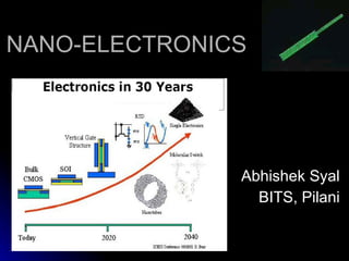
- 1. NANO-ELECTRONICS Abhishek Syal BITS, Pilani
- 7. Computing Devices CMOS Devices Solid State Devices Molecular Devices Nano CMOS Quantum Dot RTD Quantum Devices CNFET SET Electro- mechanical Photoactive Quantum Electro- chemical
- 10. Si Nanotransistor(Berkeley Device gp) Hot Spots in Si nanotransistors! Gate Gate Source Drain Nanowire Channel Metallic Carbon Nanotubes: Conducting Wires Semiconducting Nanotubes: Transistors nano-scale circuits ! 1 nm transistor!
- 11. Nanotubes/wires: CNT DNA Inorganic Si, Cu, vanadium oxide , Thermal conductivity ~ 3000 W / mK in the axial direction with small values in the radial direction & Very high current carrying capacity
- 12. Current focus is to grow 1-d nanowires Motivation • One-dimensional quantum confinement • Bandgap varies with wire diameter • Single crystal with well-defined surface structural properties • Tunable electronic properties by doping • Truly bottom-up integration possible Various Inorganic Nanowires Down to 0.4 eV
- 13. Electrical interconnects Copper, Tungsten Photonics (Q-switch, blue-green laser diode, blue-UV photodetector) Zinc Selenide Electronics, optoelectronics Indium Phosphide Insulator Boron Nitride High temperature electronics, UV detectors and lasers, automotive electronics and sensors Wide Bandgap Nitrides (GaN) Field emission device Copper Oxide UV laser, field emission device, chemical sensor Zinc Oxide Transparent conductive film in display electrodes, solar cells, organic light emitting diodes Indium Tin Oxide Chemical sensors, biosensors Indium Oxide Chemical sensors Tin Oxide Electronics, IR detectors Germanium Electronics, sensors Silicon APPLICATION MATERIAL
- 14. Nanotube Logic Circuits (Logic Gate Implementation using nanoCMOS) Nanotube Logic (Avouris et al ., IBM) What next ???
- 15. Can we scale down further ???
- 16. Computing Devices CMOS Devices Solid State Devices Molecular Devices Nano CMOS Quantum Dot RTD Quantum Devices CNFET SET Electro- mechanical Photoactive Quantum Electro- chemical
- 19. An Atomic Relay
- 21. (001)
- 22. THANK YOU :-) [email_address]
- 29. TubeFET (McEuen et al ., Berkeley)