SlideShare une entreprise Scribd logo
1  sur  28
Three FPLD Types
• Simple Programmable Logic Device (SPLD)
  – LSI device
  – Less than 1000 logic gates
• Complex Programmable Logic Device (CPLD)
  – VLSI device
  – Higher logic capacity than SPLDs
• Field Programmable Gate Array (FPGA)
  – VLSI device
  – Higher logic capacity than CPLDs

                                                      Programmable
                                                      Logic Devices
                                                         (FPLDs)


                                          SPLDs          CPLDs            FPGAs
                                       (e.g., PALs)


                                                                      1
Three FPLD Types
• Simple Programmable Logic Device (SPLD)
  – PLA or PAL
  – Fixed internal routing, deterministic propagation delays
• Complex Programmable Logic Device (CPLD)
  – Multiple SPLDs onto a single chip
  – Programmable interconnect
• Field Programmable Gate Array (FPGA)
  – An array of logic blocks
  – Large number of gates, user selectable interconnection,
    delays depending on design and routing
                                                        Programmable
  – A high ratio of flip-flops to logic resources       Logic Devices
                                                           (FPLDs)


                                            SPLDs          CPLDs            FPGAs
                                         (e.g., PALs)


                                                                        2
SPLDs
• SPLDs = Simple PLDs
• Popular SPLD Architecture Types
  – Programmable Logic Array, PLA
  – Programmable Array Logic, PAL (Vantis)
  – General Array Logic, GAL (Lattice)
  – others
• Architecture Differences
  – AND versus OR implementation
  – Programmability (e.g., EE)
  – Fundamental logic block                       Programmable
                                                  Logic Devices
                                                     (FPLDs)


                                      SPLDs          CPLDs            FPGAs
                                   (e.g., PALs)


                                                                  3
SPLDs
                                   • We have already taken a close
                                     look at SPLDs
                                   • A PLA-like SPLD is illustrated
                                     at left
                                     – PAL and GAL devices offered a
                Logic Functions
                                       somewhat better solution
                                   • SPLDs are good alternative to
                   Sums
                                     using SSI and MSI devices
                                     – Especially if re-programmable

                                                             Programmable
                                                             Logic Devices
                                                                (FPLDs)

Product Terms

                                                 SPLDs          CPLDs            FPGAs
                                              (e.g., PALs)


                                                                             4
SPLDs
• Conventional programmable logic
  – PALs, PLAs, GALs
  – standard parts like GAL22V10 and PAL16R4 are available from
    multiple vendors
• Includes programmable logic cells to a limited degree
  (programming options in I/O cells, may have fixed
  AND/OR gates for logic), limited routing network
• Lowest density of all programmable devices, however,
  can offer very high performance
• SPLDs have nearly replaced
  TTL logic which was the                               Programmable
                                                        Logic Devices

  dominate approach to logic                               (FPLDs)


  implementation                        SPLDs              CPLDs            FPGAs
                                         (e.g., PALs)


                                                                        5
How to Expand SPLD Architecture?
• Increase number of inputs and outputs in a
  conventional PLD?
  – e.g., 16V8 → 20V8 → 22V10
  – Why not → 32V16 → 128V64 ?
• Problems:
  – n times the number of inputs and outputs requires n2 as
    much chip area – too costly
  – logic gets slower as number of inputs to AND array
    increases

                                                       Programmable
                                                       Logic Devices
                                                          (FPLDs)


                                           SPLDs          CPLDs            FPGAs
                                        (e.g., PALs)


                                                                       6
How to Expand SPLD Architecture?
• Solution:
  – Multiple SPLDs with a relatively small programmable
    interconnect
  – Less general than a single large PLD
  – Can use software “fitter” to partition into smaller PLD blocks


                                                        Programmable
                                                        Logic Devices
                                                           (FPLDs)


      CPLD Architecture
                                            SPLDs          CPLDs            FPGAs
                                         (e.g., PALs)


                                                                        7
CPLDs
• PALs and GALs are available only in small sizes
  – equivalent to a few hundred logic gates
• For bigger logic circuits, complex PLDs or CPLDs can
  be used.
• CPLDs contain the equivalent of several PALs/GALs
  – linked by programmable interconnections
  – all in one integrated circuit (IC)
• CPLDs can replace thousands, or even hundreds of
  thousands, of individual logic gates
  – increased integration density

                                                             Programmable
                                                             Logic Devices
                                                                (FPLDs)


                                                 SPLDs          CPLDs            FPGAs
                                              (e.g., PALs)


                                                                             8
Complex PLDs
• Some CPLDs are programmed using a PAL
  programmer, but this method becomes inconvenient
  for devices with hundreds of pins.
• A second method of programming is to solder the
  device to its printed circuit board, then feed it with a
  serial data stream from a personal computer.
• The CPLD contains a circuit that decodes the data
  stream and configures the CPLD to perform its
  specified logic function.

                                                       Programmable
                                                       Logic Devices
                                                          (FPLDs)


                                           SPLDs          CPLDs            FPGAs
                                        (e.g., PALs)


                                                                       9
Complex PLDs versus FPGAs
• Xilinx, for example:
• Xilinx CPLD devices that are cheaper and have fewer
  gates than Xilinx FPGAs
• Meant for interfacing rather than heavy computation
• Built-in flash memory
  – Compare to FPGA which needs external configuration
    memory
• Xess board has XC9572XL part
  – Approximately $2-$7 in quantities of one
  – vs. ~$15-20 for the Spartan2 FPGA on the board
  – Larger quantities much lower
  – 1600 gates, 72 registers
                                                     Programmable
                                                     Logic Devices
                                                        (FPLDs)


                                         SPLDs          CPLDs             FPGAs
                                      (e.g., PALs)


                                                                     10
CPLD Architecture
• Simplified CPLD
  architecture
• Small number of largish
  PLDs (e.g., “36V18”) on a
  single chip
• Programmable
  interconnect between
  PLDs
• Large number of I/O
  blocks
• Large number of pins


                                  11
CPLDs
• Composition of Complex PLDs
  – typically composed of 2-64 SPLDs
  – interconnected using sophisticated logic
  – includes macrocells (more about these later)
  – includes input/output blocks
• Economical for designing large systems
• Fast – switching speed


                                                      Programmable
                                                      Logic Devices
                                                         (FPLDs)


                                          SPLDs          CPLDs             FPGAs
                                       (e.g., PALs)


                                                                      12
CPLDs
• Complex PLD's have arrays of PLD's on one chip, with
  an interconnection matrix connecting them.
• Timing performance can be more predictable than
  FPGAs because of simpler interconnect structure.
• Density is normally less than most FPGAs (although
  high end CPLDs will have about the same density as
  low-end FPGAs).
• Performance of CPLDs is
  usually better than FPGAs,
  but depends on vendor,
  number of cells in CPLD, and                    Programmable
                                                  Logic Devices
                                                     (FPLDs)

  compared FPGA.
                                      SPLDs          CPLDs             FPGAs
                                   (e.g., PALs)


                                                                  13
CPLD Families
• Identical individual PLD blocks (Xilinx “FBs”) replicated
  in different family members
  – Different number of PLD blocks
  – Different number of I/O pins


                                                 Xilinx
                                                 XC9500
                                                 CPLD
                                                 Series


                                                         14
Typical CPLD Packages
• CPLDs are made using 2 to 64 SPLDs
• Packages use 44-pins to over 200-pins (or more)


                                                    15
Typical CPLD Packages
• QFP = Quad Flat Package
– A QFP is an IC package with leads extending from each of
  the four sides.
– It is used primarily for surface mounting, no socketing
• TQFP = Thin Quad Flat Package
• PQFP = Plastic Quad Flat Package
• VQFP = Very small Quad Flat Package

• PLCC = Plastic Leaded Chip Carrier
– A package related to QFP
– Similar but has pins with larger distance, curved up
  underneath a thicker body to simplify socketing

                                                         16
CPLD Package Types
• CSP = Chip Scale Package
  – IC package with an area no greater than 1.2 times that
    of the die


• BGA = Ball Grid Array
  – A type of surface-mount packaging used for ICs
  – Pins are replaced by balls of solder stuck to the bottom
    of the package
  – The device is placed on a PCB that carries copper pads
    in a pattern that matches the solder balls
  – The assembly is then heated causing the solder balls to
    melt


                                                             17
CPLD Families
• Many CPLDs have fewer
  I/O pins than macrocells
  – “Buried” Macrocells – provide
    needed logic terms internally
    but these outputs are not
    connected externally
  – IC package size dictates
    number of I/O pins but not
    the total number of
    macrocells
  – Typical CPLD families have devices with differing
    resources in the same IC package


                                                        18
Xilinx CPLDs
• Notice overlap in resource availability in a particular
  package.


                                                            19
XC9572 CPLD Part Numbers
• The part number for Xilinx CPLD devices includes
  information as follows:


                                                     20
XC9500 CPLD Block Diagram
• The XC9500 CPLD
  family provides
  advanced in-system
  programming and test
  capabilities for high
  performance, general
  purpose logic
  integration.
• All devices are in-
  system programmable
  for a minimum of
  10,000 program/erase
  cycles.

                                 21
9500-Family Function Blocks (FBs)
• 18 macrocells per FB
• 36 inputs per FB (partitioning challenge, but also
  reason for relatively compact size of FBs)
• Macrocell outputs can go to I/O cells or back into
  switch matrix to be routed to this or other FBs


                                                       22
9500-Series Macrocell
 • 18 macrocells per Function Block

                       Set control

        Programmable inversion
            or XOR product term


            Up to 5 product terms

Global clock or product-term clock


                    Reset control


                       OE control

                                        23
9500-Series Product-Term Allocator
  • Share terms from above and below


programmable
steering
elements


                                       24
XC9500 Family
• An I/O block is composed of
  input buffer, output buffer,
  multiplexer for the output
  control and grounding control
• Slew rate control is used to
  smooth the rising and the falling
  edges of the output pulse.
• Grounding control is used to
  make the input/output pin (I/O)
  an earth ground (noise
  suppression).
• Each input/output pin can handle a 24-mA current.


                                                      25
9500-Series I/O Block
• OE Multiplexer (OE
  MUX) controls an output
  enable or stop.
• It is controlled by the
  signal from the macrocell
  or the signal from the
  GTS (Global Three-State
  control) pin.
• There are four
  GTS in XC95216
  and XC95288
  two in the
  others.

                                   26
Switch Matrix for XC95108
• Could be anything from a limited set of multiplexers to
  a full crossbar
  – Multiplexer -- small, fast, but difficult fitting
  – Crossbar -- easy fitting but large and slow


                                                        27
Problems with CPLDs
• Pin locking
  – Small changes, and certainly large ones, can cause the
    fitter to pick a different allocation of I/O blocks and pinout
  – Locking too early may make the resulting circuit slower
    or not fit at all
• Running out of resources
  – Design may “blow up” if it doesn’t all fit on a single
    device
  – On-chip interconnect resources are much richer than off-
    chip
  – Larger devices are exponentially more expensive


                                                                28

Contenu connexe

Tendances

Design of LDPC Decoder Based On FPGA in Digital Image Watermarking Technology
Design of LDPC Decoder Based On FPGA in Digital Image Watermarking TechnologyDesign of LDPC Decoder Based On FPGA in Digital Image Watermarking Technology
Design of LDPC Decoder Based On FPGA in Digital Image Watermarking TechnologyTELKOMNIKA JOURNAL
 
Xilinx virtex 7 fpga - Semester Presentation
Xilinx virtex 7 fpga - Semester PresentationXilinx virtex 7 fpga - Semester Presentation
Xilinx virtex 7 fpga - Semester PresentationMuhammad Muzaffar Khan
 
FPGA_Overview_Ibr_2014
FPGA_Overview_Ibr_2014FPGA_Overview_Ibr_2014
FPGA_Overview_Ibr_2014Ibrahim Hejab
 
TRACK F: OpenCL for ALTERA FPGAs, Accelerating performance and design product...
TRACK F: OpenCL for ALTERA FPGAs, Accelerating performance and design product...TRACK F: OpenCL for ALTERA FPGAs, Accelerating performance and design product...
TRACK F: OpenCL for ALTERA FPGAs, Accelerating performance and design product...chiportal
 
Implementation of Soft-core processor on FPGA (Final Presentation)
Implementation of Soft-core processor on FPGA (Final Presentation)Implementation of Soft-core processor on FPGA (Final Presentation)
Implementation of Soft-core processor on FPGA (Final Presentation)Deepak Kumar
 
SoC~FPGA~ASIC~Embedded
SoC~FPGA~ASIC~EmbeddedSoC~FPGA~ASIC~Embedded
SoC~FPGA~ASIC~EmbeddedChili.CHIPS
 
Fpga asic technologies_flow
Fpga asic technologies_flowFpga asic technologies_flow
Fpga asic technologies_flowravi4all
 
A review on virtex fpga family from xilinx
A review on virtex fpga family from xilinxA review on virtex fpga family from xilinx
A review on virtex fpga family from xilinxUniversity of Kassel
 
Fpga Device Selection
Fpga Device SelectionFpga Device Selection
Fpga Device SelectionVikram Singh
 
Traditional vs. SoC FPGA Design Flow A Video Pipeline Case Study
Traditional vs. SoC FPGA Design Flow A Video Pipeline Case StudyTraditional vs. SoC FPGA Design Flow A Video Pipeline Case Study
Traditional vs. SoC FPGA Design Flow A Video Pipeline Case StudyAltera Corporation
 
Digital VLSI Design and FPGA Implementation
Digital VLSI Design and FPGA ImplementationDigital VLSI Design and FPGA Implementation
Digital VLSI Design and FPGA ImplementationAmber Bhaumik
 
FPGA TECHNOLOGY AND FAMILIES
FPGA TECHNOLOGY AND FAMILIESFPGA TECHNOLOGY AND FAMILIES
FPGA TECHNOLOGY AND FAMILIESrevathilakshmi2
 
The comparison between FPGA , ARDUINO , ASIC
The comparison between FPGA , ARDUINO , ASIC The comparison between FPGA , ARDUINO , ASIC
The comparison between FPGA , ARDUINO , ASIC Mohamed Youssery
 

Tendances (20)

Design of LDPC Decoder Based On FPGA in Digital Image Watermarking Technology
Design of LDPC Decoder Based On FPGA in Digital Image Watermarking TechnologyDesign of LDPC Decoder Based On FPGA in Digital Image Watermarking Technology
Design of LDPC Decoder Based On FPGA in Digital Image Watermarking Technology
 
FPGA In a Nutshell
FPGA In a NutshellFPGA In a Nutshell
FPGA In a Nutshell
 
Fpga technology
Fpga technologyFpga technology
Fpga technology
 
Xilinx virtex 7 fpga - Semester Presentation
Xilinx virtex 7 fpga - Semester PresentationXilinx virtex 7 fpga - Semester Presentation
Xilinx virtex 7 fpga - Semester Presentation
 
FPGA_Overview_Ibr_2014
FPGA_Overview_Ibr_2014FPGA_Overview_Ibr_2014
FPGA_Overview_Ibr_2014
 
TRACK F: OpenCL for ALTERA FPGAs, Accelerating performance and design product...
TRACK F: OpenCL for ALTERA FPGAs, Accelerating performance and design product...TRACK F: OpenCL for ALTERA FPGAs, Accelerating performance and design product...
TRACK F: OpenCL for ALTERA FPGAs, Accelerating performance and design product...
 
FPGA workshop
FPGA workshopFPGA workshop
FPGA workshop
 
Fpga 03-cpld-and-fpga
Fpga 03-cpld-and-fpgaFpga 03-cpld-and-fpga
Fpga 03-cpld-and-fpga
 
Implementation of Soft-core processor on FPGA (Final Presentation)
Implementation of Soft-core processor on FPGA (Final Presentation)Implementation of Soft-core processor on FPGA (Final Presentation)
Implementation of Soft-core processor on FPGA (Final Presentation)
 
SoC~FPGA~ASIC~Embedded
SoC~FPGA~ASIC~EmbeddedSoC~FPGA~ASIC~Embedded
SoC~FPGA~ASIC~Embedded
 
Fpga asic technologies_flow
Fpga asic technologies_flowFpga asic technologies_flow
Fpga asic technologies_flow
 
A review on virtex fpga family from xilinx
A review on virtex fpga family from xilinxA review on virtex fpga family from xilinx
A review on virtex fpga family from xilinx
 
Fpga in space
Fpga in spaceFpga in space
Fpga in space
 
Fpga Device Selection
Fpga Device SelectionFpga Device Selection
Fpga Device Selection
 
Programmable Devices En 01
Programmable Devices En 01Programmable Devices En 01
Programmable Devices En 01
 
Traditional vs. SoC FPGA Design Flow A Video Pipeline Case Study
Traditional vs. SoC FPGA Design Flow A Video Pipeline Case StudyTraditional vs. SoC FPGA Design Flow A Video Pipeline Case Study
Traditional vs. SoC FPGA Design Flow A Video Pipeline Case Study
 
Digital VLSI Design and FPGA Implementation
Digital VLSI Design and FPGA ImplementationDigital VLSI Design and FPGA Implementation
Digital VLSI Design and FPGA Implementation
 
Chapter 4
Chapter 4Chapter 4
Chapter 4
 
FPGA TECHNOLOGY AND FAMILIES
FPGA TECHNOLOGY AND FAMILIESFPGA TECHNOLOGY AND FAMILIES
FPGA TECHNOLOGY AND FAMILIES
 
The comparison between FPGA , ARDUINO , ASIC
The comparison between FPGA , ARDUINO , ASIC The comparison between FPGA , ARDUINO , ASIC
The comparison between FPGA , ARDUINO , ASIC
 

En vedette

VHDL - Enumerated Types (Part 3)
VHDL - Enumerated Types (Part 3)VHDL - Enumerated Types (Part 3)
VHDL - Enumerated Types (Part 3)Abhilash Nair
 
Introduction to VHDL - Part 1
Introduction to VHDL - Part 1Introduction to VHDL - Part 1
Introduction to VHDL - Part 1Abhilash Nair
 
Synchronous design process
Synchronous design processSynchronous design process
Synchronous design processAbhilash Nair
 
Sequential Circuits - Flip Flops (Part 1)
Sequential Circuits - Flip Flops (Part 1)Sequential Circuits - Flip Flops (Part 1)
Sequential Circuits - Flip Flops (Part 1)Abhilash Nair
 
State Machine Design and Synthesis
State Machine Design and SynthesisState Machine Design and Synthesis
State Machine Design and SynthesisAbhilash Nair
 
Designing Clocked Synchronous State Machine
Designing Clocked Synchronous State MachineDesigning Clocked Synchronous State Machine
Designing Clocked Synchronous State MachineAbhilash Nair
 
Sequential Circuits - Flip Flops
Sequential Circuits - Flip FlopsSequential Circuits - Flip Flops
Sequential Circuits - Flip FlopsAbhilash Nair
 
Sequential Circuits - Flip Flops (Part 2)
Sequential Circuits - Flip Flops (Part 2)Sequential Circuits - Flip Flops (Part 2)
Sequential Circuits - Flip Flops (Part 2)Abhilash Nair
 
Static and Dynamic Read/Write memories
Static and Dynamic Read/Write memoriesStatic and Dynamic Read/Write memories
Static and Dynamic Read/Write memoriesAbhilash Nair
 
Analysis of state machines & Conversion of models
Analysis of state machines & Conversion of modelsAnalysis of state machines & Conversion of models
Analysis of state machines & Conversion of modelsAbhilash Nair
 
Analysis of state machines
Analysis of state machinesAnalysis of state machines
Analysis of state machinesAbhilash Nair
 

En vedette (16)

VHDL - Enumerated Types (Part 3)
VHDL - Enumerated Types (Part 3)VHDL - Enumerated Types (Part 3)
VHDL - Enumerated Types (Part 3)
 
Introduction to VHDL - Part 1
Introduction to VHDL - Part 1Introduction to VHDL - Part 1
Introduction to VHDL - Part 1
 
VHDL - Part 2
VHDL - Part 2VHDL - Part 2
VHDL - Part 2
 
Synchronous design process
Synchronous design processSynchronous design process
Synchronous design process
 
VHDL Part 4
VHDL Part 4VHDL Part 4
VHDL Part 4
 
Sequential Circuits - Flip Flops (Part 1)
Sequential Circuits - Flip Flops (Part 1)Sequential Circuits - Flip Flops (Part 1)
Sequential Circuits - Flip Flops (Part 1)
 
State Machine Design and Synthesis
State Machine Design and SynthesisState Machine Design and Synthesis
State Machine Design and Synthesis
 
Designing Clocked Synchronous State Machine
Designing Clocked Synchronous State MachineDesigning Clocked Synchronous State Machine
Designing Clocked Synchronous State Machine
 
Sequential Circuits - Flip Flops
Sequential Circuits - Flip FlopsSequential Circuits - Flip Flops
Sequential Circuits - Flip Flops
 
MSI Shift Registers
MSI Shift RegistersMSI Shift Registers
MSI Shift Registers
 
Sequential Circuits - Flip Flops (Part 2)
Sequential Circuits - Flip Flops (Part 2)Sequential Circuits - Flip Flops (Part 2)
Sequential Circuits - Flip Flops (Part 2)
 
Static and Dynamic Read/Write memories
Static and Dynamic Read/Write memoriesStatic and Dynamic Read/Write memories
Static and Dynamic Read/Write memories
 
FPGA
FPGAFPGA
FPGA
 
DRAM
DRAMDRAM
DRAM
 
Analysis of state machines & Conversion of models
Analysis of state machines & Conversion of modelsAnalysis of state machines & Conversion of models
Analysis of state machines & Conversion of models
 
Analysis of state machines
Analysis of state machinesAnalysis of state machines
Analysis of state machines
 

Similaire à FPLDs

Fundamentals of FPGA
Fundamentals of FPGAFundamentals of FPGA
Fundamentals of FPGAvelamakuri
 
Architecture of fpg as and cplds
Architecture of fpg as and cpldsArchitecture of fpg as and cplds
Architecture of fpg as and cpldsmikeproud
 
L12 programmable+logic+devices+(pld)
L12 programmable+logic+devices+(pld)L12 programmable+logic+devices+(pld)
L12 programmable+logic+devices+(pld)NAGASAI547
 
L12_PROGRAMMABLE+LOGIC+DEVICES+(PLD).ppt
L12_PROGRAMMABLE+LOGIC+DEVICES+(PLD).pptL12_PROGRAMMABLE+LOGIC+DEVICES+(PLD).ppt
L12_PROGRAMMABLE+LOGIC+DEVICES+(PLD).pptMikeTango5
 
Programmable Logic Devices Plds
Programmable Logic Devices PldsProgrammable Logic Devices Plds
Programmable Logic Devices PldsGaditek
 
Cpld and fpga mod vi
Cpld and fpga   mod viCpld and fpga   mod vi
Cpld and fpga mod viAgi George
 
Programmable Hardware - An Overview
Programmable Hardware - An OverviewProgrammable Hardware - An Overview
Programmable Hardware - An OverviewS Yousuf Imam
 
1. FPGA architectures.pdf
1. FPGA architectures.pdf1. FPGA architectures.pdf
1. FPGA architectures.pdfTesfuFiseha1
 
Programmable lrray Logic
Programmable lrray LogicProgrammable lrray Logic
Programmable lrray Logicrohitladdu
 
FPGA Intro
FPGA IntroFPGA Intro
FPGA Intronaito88
 

Similaire à FPLDs (20)

1.CPLD SPLD.pdf
1.CPLD SPLD.pdf1.CPLD SPLD.pdf
1.CPLD SPLD.pdf
 
PLDs
PLDsPLDs
PLDs
 
PLD's.pptx
PLD's.pptxPLD's.pptx
PLD's.pptx
 
Programable logic devices (1)
Programable logic devices (1)Programable logic devices (1)
Programable logic devices (1)
 
Fundamentals of FPGA
Fundamentals of FPGAFundamentals of FPGA
Fundamentals of FPGA
 
Architecture of fpg as and cplds
Architecture of fpg as and cpldsArchitecture of fpg as and cplds
Architecture of fpg as and cplds
 
Lecture syn 024.cpld-fpga
Lecture syn 024.cpld-fpgaLecture syn 024.cpld-fpga
Lecture syn 024.cpld-fpga
 
L12 programmable+logic+devices+(pld)
L12 programmable+logic+devices+(pld)L12 programmable+logic+devices+(pld)
L12 programmable+logic+devices+(pld)
 
L12_PROGRAMMABLE+LOGIC+DEVICES+(PLD).ppt
L12_PROGRAMMABLE+LOGIC+DEVICES+(PLD).pptL12_PROGRAMMABLE+LOGIC+DEVICES+(PLD).ppt
L12_PROGRAMMABLE+LOGIC+DEVICES+(PLD).ppt
 
module7.pptx
module7.pptxmodule7.pptx
module7.pptx
 
Programmable Logic Devices Plds
Programmable Logic Devices PldsProgrammable Logic Devices Plds
Programmable Logic Devices Plds
 
Cpld and fpga mod vi
Cpld and fpga   mod viCpld and fpga   mod vi
Cpld and fpga mod vi
 
UNIT-1.pptx
UNIT-1.pptxUNIT-1.pptx
UNIT-1.pptx
 
Programmable Hardware - An Overview
Programmable Hardware - An OverviewProgrammable Hardware - An Overview
Programmable Hardware - An Overview
 
Pld dp
Pld dpPld dp
Pld dp
 
Asic vs fpga
Asic vs fpgaAsic vs fpga
Asic vs fpga
 
1. FPGA architectures.pdf
1. FPGA architectures.pdf1. FPGA architectures.pdf
1. FPGA architectures.pdf
 
Flash memory
Flash memoryFlash memory
Flash memory
 
Programmable lrray Logic
Programmable lrray LogicProgrammable lrray Logic
Programmable lrray Logic
 
FPGA Intro
FPGA IntroFPGA Intro
FPGA Intro
 

Plus de Abhilash Nair

Plus de Abhilash Nair (11)

Feedback Sequential Circuits
Feedback Sequential CircuitsFeedback Sequential Circuits
Feedback Sequential Circuits
 
Designing State Machine
Designing State MachineDesigning State Machine
Designing State Machine
 
Documentation Standards of an IC
Documentation Standards of an ICDocumentation Standards of an IC
Documentation Standards of an IC
 
Shift Registers
Shift RegistersShift Registers
Shift Registers
 
MSI Counters
MSI CountersMSI Counters
MSI Counters
 
EPROM, PROM & ROM
EPROM, PROM & ROMEPROM, PROM & ROM
EPROM, PROM & ROM
 
Counters
CountersCounters
Counters
 
Trends Of Televisions
Trends Of TelevisionsTrends Of Televisions
Trends Of Televisions
 
Core java slides
Core java slidesCore java slides
Core java slides
 
Vectors in Java
Vectors in JavaVectors in Java
Vectors in Java
 
Arrays in Java
Arrays in JavaArrays in Java
Arrays in Java
 

Dernier

A Critique of the Proposed National Education Policy Reform
A Critique of the Proposed National Education Policy ReformA Critique of the Proposed National Education Policy Reform
A Critique of the Proposed National Education Policy ReformChameera Dedduwage
 
Software Engineering Methodologies (overview)
Software Engineering Methodologies (overview)Software Engineering Methodologies (overview)
Software Engineering Methodologies (overview)eniolaolutunde
 
Separation of Lanthanides/ Lanthanides and Actinides
Separation of Lanthanides/ Lanthanides and ActinidesSeparation of Lanthanides/ Lanthanides and Actinides
Separation of Lanthanides/ Lanthanides and ActinidesFatimaKhan178732
 
Industrial Policy - 1948, 1956, 1973, 1977, 1980, 1991
Industrial Policy - 1948, 1956, 1973, 1977, 1980, 1991Industrial Policy - 1948, 1956, 1973, 1977, 1980, 1991
Industrial Policy - 1948, 1956, 1973, 1977, 1980, 1991RKavithamani
 
POINT- BIOCHEMISTRY SEM 2 ENZYMES UNIT 5.pptx
POINT- BIOCHEMISTRY SEM 2 ENZYMES UNIT 5.pptxPOINT- BIOCHEMISTRY SEM 2 ENZYMES UNIT 5.pptx
POINT- BIOCHEMISTRY SEM 2 ENZYMES UNIT 5.pptxSayali Powar
 
Student login on Anyboli platform.helpin
Student login on Anyboli platform.helpinStudent login on Anyboli platform.helpin
Student login on Anyboli platform.helpinRaunakKeshri1
 
Nutritional Needs Presentation - HLTH 104
Nutritional Needs Presentation - HLTH 104Nutritional Needs Presentation - HLTH 104
Nutritional Needs Presentation - HLTH 104misteraugie
 
URLs and Routing in the Odoo 17 Website App
URLs and Routing in the Odoo 17 Website AppURLs and Routing in the Odoo 17 Website App
URLs and Routing in the Odoo 17 Website AppCeline George
 
How to Make a Pirate ship Primary Education.pptx
How to Make a Pirate ship Primary Education.pptxHow to Make a Pirate ship Primary Education.pptx
How to Make a Pirate ship Primary Education.pptxmanuelaromero2013
 
Presentation by Andreas Schleicher Tackling the School Absenteeism Crisis 30 ...
Presentation by Andreas Schleicher Tackling the School Absenteeism Crisis 30 ...Presentation by Andreas Schleicher Tackling the School Absenteeism Crisis 30 ...
Presentation by Andreas Schleicher Tackling the School Absenteeism Crisis 30 ...EduSkills OECD
 
Organic Name Reactions for the students and aspirants of Chemistry12th.pptx
Organic Name Reactions  for the students and aspirants of Chemistry12th.pptxOrganic Name Reactions  for the students and aspirants of Chemistry12th.pptx
Organic Name Reactions for the students and aspirants of Chemistry12th.pptxVS Mahajan Coaching Centre
 
Sanyam Choudhary Chemistry practical.pdf
Sanyam Choudhary Chemistry practical.pdfSanyam Choudhary Chemistry practical.pdf
Sanyam Choudhary Chemistry practical.pdfsanyamsingh5019
 
BASLIQ CURRENT LOOKBOOK LOOKBOOK(1) (1).pdf
BASLIQ CURRENT LOOKBOOK  LOOKBOOK(1) (1).pdfBASLIQ CURRENT LOOKBOOK  LOOKBOOK(1) (1).pdf
BASLIQ CURRENT LOOKBOOK LOOKBOOK(1) (1).pdfSoniaTolstoy
 
The Most Excellent Way | 1 Corinthians 13
The Most Excellent Way | 1 Corinthians 13The Most Excellent Way | 1 Corinthians 13
The Most Excellent Way | 1 Corinthians 13Steve Thomason
 
The basics of sentences session 2pptx copy.pptx
The basics of sentences session 2pptx copy.pptxThe basics of sentences session 2pptx copy.pptx
The basics of sentences session 2pptx copy.pptxheathfieldcps1
 
SOCIAL AND HISTORICAL CONTEXT - LFTVD.pptx
SOCIAL AND HISTORICAL CONTEXT - LFTVD.pptxSOCIAL AND HISTORICAL CONTEXT - LFTVD.pptx
SOCIAL AND HISTORICAL CONTEXT - LFTVD.pptxiammrhaywood
 
Advanced Views - Calendar View in Odoo 17
Advanced Views - Calendar View in Odoo 17Advanced Views - Calendar View in Odoo 17
Advanced Views - Calendar View in Odoo 17Celine George
 

Dernier (20)

Staff of Color (SOC) Retention Efforts DDSD
Staff of Color (SOC) Retention Efforts DDSDStaff of Color (SOC) Retention Efforts DDSD
Staff of Color (SOC) Retention Efforts DDSD
 
A Critique of the Proposed National Education Policy Reform
A Critique of the Proposed National Education Policy ReformA Critique of the Proposed National Education Policy Reform
A Critique of the Proposed National Education Policy Reform
 
Software Engineering Methodologies (overview)
Software Engineering Methodologies (overview)Software Engineering Methodologies (overview)
Software Engineering Methodologies (overview)
 
Separation of Lanthanides/ Lanthanides and Actinides
Separation of Lanthanides/ Lanthanides and ActinidesSeparation of Lanthanides/ Lanthanides and Actinides
Separation of Lanthanides/ Lanthanides and Actinides
 
Industrial Policy - 1948, 1956, 1973, 1977, 1980, 1991
Industrial Policy - 1948, 1956, 1973, 1977, 1980, 1991Industrial Policy - 1948, 1956, 1973, 1977, 1980, 1991
Industrial Policy - 1948, 1956, 1973, 1977, 1980, 1991
 
POINT- BIOCHEMISTRY SEM 2 ENZYMES UNIT 5.pptx
POINT- BIOCHEMISTRY SEM 2 ENZYMES UNIT 5.pptxPOINT- BIOCHEMISTRY SEM 2 ENZYMES UNIT 5.pptx
POINT- BIOCHEMISTRY SEM 2 ENZYMES UNIT 5.pptx
 
Student login on Anyboli platform.helpin
Student login on Anyboli platform.helpinStudent login on Anyboli platform.helpin
Student login on Anyboli platform.helpin
 
Nutritional Needs Presentation - HLTH 104
Nutritional Needs Presentation - HLTH 104Nutritional Needs Presentation - HLTH 104
Nutritional Needs Presentation - HLTH 104
 
URLs and Routing in the Odoo 17 Website App
URLs and Routing in the Odoo 17 Website AppURLs and Routing in the Odoo 17 Website App
URLs and Routing in the Odoo 17 Website App
 
How to Make a Pirate ship Primary Education.pptx
How to Make a Pirate ship Primary Education.pptxHow to Make a Pirate ship Primary Education.pptx
How to Make a Pirate ship Primary Education.pptx
 
Presentation by Andreas Schleicher Tackling the School Absenteeism Crisis 30 ...
Presentation by Andreas Schleicher Tackling the School Absenteeism Crisis 30 ...Presentation by Andreas Schleicher Tackling the School Absenteeism Crisis 30 ...
Presentation by Andreas Schleicher Tackling the School Absenteeism Crisis 30 ...
 
Mattingly "AI & Prompt Design: Structured Data, Assistants, & RAG"
Mattingly "AI & Prompt Design: Structured Data, Assistants, & RAG"Mattingly "AI & Prompt Design: Structured Data, Assistants, & RAG"
Mattingly "AI & Prompt Design: Structured Data, Assistants, & RAG"
 
Organic Name Reactions for the students and aspirants of Chemistry12th.pptx
Organic Name Reactions  for the students and aspirants of Chemistry12th.pptxOrganic Name Reactions  for the students and aspirants of Chemistry12th.pptx
Organic Name Reactions for the students and aspirants of Chemistry12th.pptx
 
Sanyam Choudhary Chemistry practical.pdf
Sanyam Choudhary Chemistry practical.pdfSanyam Choudhary Chemistry practical.pdf
Sanyam Choudhary Chemistry practical.pdf
 
BASLIQ CURRENT LOOKBOOK LOOKBOOK(1) (1).pdf
BASLIQ CURRENT LOOKBOOK  LOOKBOOK(1) (1).pdfBASLIQ CURRENT LOOKBOOK  LOOKBOOK(1) (1).pdf
BASLIQ CURRENT LOOKBOOK LOOKBOOK(1) (1).pdf
 
TataKelola dan KamSiber Kecerdasan Buatan v022.pdf
TataKelola dan KamSiber Kecerdasan Buatan v022.pdfTataKelola dan KamSiber Kecerdasan Buatan v022.pdf
TataKelola dan KamSiber Kecerdasan Buatan v022.pdf
 
The Most Excellent Way | 1 Corinthians 13
The Most Excellent Way | 1 Corinthians 13The Most Excellent Way | 1 Corinthians 13
The Most Excellent Way | 1 Corinthians 13
 
The basics of sentences session 2pptx copy.pptx
The basics of sentences session 2pptx copy.pptxThe basics of sentences session 2pptx copy.pptx
The basics of sentences session 2pptx copy.pptx
 
SOCIAL AND HISTORICAL CONTEXT - LFTVD.pptx
SOCIAL AND HISTORICAL CONTEXT - LFTVD.pptxSOCIAL AND HISTORICAL CONTEXT - LFTVD.pptx
SOCIAL AND HISTORICAL CONTEXT - LFTVD.pptx
 
Advanced Views - Calendar View in Odoo 17
Advanced Views - Calendar View in Odoo 17Advanced Views - Calendar View in Odoo 17
Advanced Views - Calendar View in Odoo 17
 

FPLDs

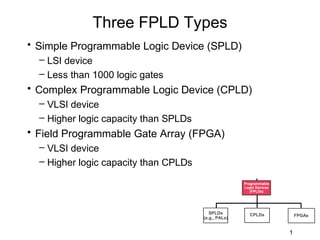
  • 1. Three FPLD Types • Simple Programmable Logic Device (SPLD) – LSI device – Less than 1000 logic gates • Complex Programmable Logic Device (CPLD) – VLSI device – Higher logic capacity than SPLDs • Field Programmable Gate Array (FPGA) – VLSI device – Higher logic capacity than CPLDs Programmable Logic Devices (FPLDs) SPLDs CPLDs FPGAs (e.g., PALs) 1
  • 2. Three FPLD Types • Simple Programmable Logic Device (SPLD) – PLA or PAL – Fixed internal routing, deterministic propagation delays • Complex Programmable Logic Device (CPLD) – Multiple SPLDs onto a single chip – Programmable interconnect • Field Programmable Gate Array (FPGA) – An array of logic blocks – Large number of gates, user selectable interconnection, delays depending on design and routing Programmable – A high ratio of flip-flops to logic resources Logic Devices (FPLDs) SPLDs CPLDs FPGAs (e.g., PALs) 2
  • 3. SPLDs • SPLDs = Simple PLDs • Popular SPLD Architecture Types – Programmable Logic Array, PLA – Programmable Array Logic, PAL (Vantis) – General Array Logic, GAL (Lattice) – others • Architecture Differences – AND versus OR implementation – Programmability (e.g., EE) – Fundamental logic block Programmable Logic Devices (FPLDs) SPLDs CPLDs FPGAs (e.g., PALs) 3
  • 4. SPLDs • We have already taken a close look at SPLDs • A PLA-like SPLD is illustrated at left – PAL and GAL devices offered a Logic Functions somewhat better solution • SPLDs are good alternative to Sums using SSI and MSI devices – Especially if re-programmable Programmable Logic Devices (FPLDs) Product Terms SPLDs CPLDs FPGAs (e.g., PALs) 4
  • 5. SPLDs • Conventional programmable logic – PALs, PLAs, GALs – standard parts like GAL22V10 and PAL16R4 are available from multiple vendors • Includes programmable logic cells to a limited degree (programming options in I/O cells, may have fixed AND/OR gates for logic), limited routing network • Lowest density of all programmable devices, however, can offer very high performance • SPLDs have nearly replaced TTL logic which was the Programmable Logic Devices dominate approach to logic (FPLDs) implementation SPLDs CPLDs FPGAs (e.g., PALs) 5
  • 6. How to Expand SPLD Architecture? • Increase number of inputs and outputs in a conventional PLD? – e.g., 16V8 → 20V8 → 22V10 – Why not → 32V16 → 128V64 ? • Problems: – n times the number of inputs and outputs requires n2 as much chip area – too costly – logic gets slower as number of inputs to AND array increases Programmable Logic Devices (FPLDs) SPLDs CPLDs FPGAs (e.g., PALs) 6
  • 7. How to Expand SPLD Architecture? • Solution: – Multiple SPLDs with a relatively small programmable interconnect – Less general than a single large PLD – Can use software “fitter” to partition into smaller PLD blocks Programmable Logic Devices (FPLDs) CPLD Architecture SPLDs CPLDs FPGAs (e.g., PALs) 7
  • 8. CPLDs • PALs and GALs are available only in small sizes – equivalent to a few hundred logic gates • For bigger logic circuits, complex PLDs or CPLDs can be used. • CPLDs contain the equivalent of several PALs/GALs – linked by programmable interconnections – all in one integrated circuit (IC) • CPLDs can replace thousands, or even hundreds of thousands, of individual logic gates – increased integration density Programmable Logic Devices (FPLDs) SPLDs CPLDs FPGAs (e.g., PALs) 8
  • 9. Complex PLDs • Some CPLDs are programmed using a PAL programmer, but this method becomes inconvenient for devices with hundreds of pins. • A second method of programming is to solder the device to its printed circuit board, then feed it with a serial data stream from a personal computer. • The CPLD contains a circuit that decodes the data stream and configures the CPLD to perform its specified logic function. Programmable Logic Devices (FPLDs) SPLDs CPLDs FPGAs (e.g., PALs) 9
  • 10. Complex PLDs versus FPGAs • Xilinx, for example: • Xilinx CPLD devices that are cheaper and have fewer gates than Xilinx FPGAs • Meant for interfacing rather than heavy computation • Built-in flash memory – Compare to FPGA which needs external configuration memory • Xess board has XC9572XL part – Approximately $2-$7 in quantities of one – vs. ~$15-20 for the Spartan2 FPGA on the board – Larger quantities much lower – 1600 gates, 72 registers Programmable Logic Devices (FPLDs) SPLDs CPLDs FPGAs (e.g., PALs) 10
  • 11. CPLD Architecture • Simplified CPLD architecture • Small number of largish PLDs (e.g., “36V18”) on a single chip • Programmable interconnect between PLDs • Large number of I/O blocks • Large number of pins 11
  • 12. CPLDs • Composition of Complex PLDs – typically composed of 2-64 SPLDs – interconnected using sophisticated logic – includes macrocells (more about these later) – includes input/output blocks • Economical for designing large systems • Fast – switching speed Programmable Logic Devices (FPLDs) SPLDs CPLDs FPGAs (e.g., PALs) 12
  • 13. CPLDs • Complex PLD's have arrays of PLD's on one chip, with an interconnection matrix connecting them. • Timing performance can be more predictable than FPGAs because of simpler interconnect structure. • Density is normally less than most FPGAs (although high end CPLDs will have about the same density as low-end FPGAs). • Performance of CPLDs is usually better than FPGAs, but depends on vendor, number of cells in CPLD, and Programmable Logic Devices (FPLDs) compared FPGA. SPLDs CPLDs FPGAs (e.g., PALs) 13
  • 14. CPLD Families • Identical individual PLD blocks (Xilinx “FBs”) replicated in different family members – Different number of PLD blocks – Different number of I/O pins Xilinx XC9500 CPLD Series 14
  • 15. Typical CPLD Packages • CPLDs are made using 2 to 64 SPLDs • Packages use 44-pins to over 200-pins (or more) 15
  • 16. Typical CPLD Packages • QFP = Quad Flat Package – A QFP is an IC package with leads extending from each of the four sides. – It is used primarily for surface mounting, no socketing • TQFP = Thin Quad Flat Package • PQFP = Plastic Quad Flat Package • VQFP = Very small Quad Flat Package • PLCC = Plastic Leaded Chip Carrier – A package related to QFP – Similar but has pins with larger distance, curved up underneath a thicker body to simplify socketing 16
  • 17. CPLD Package Types • CSP = Chip Scale Package – IC package with an area no greater than 1.2 times that of the die • BGA = Ball Grid Array – A type of surface-mount packaging used for ICs – Pins are replaced by balls of solder stuck to the bottom of the package – The device is placed on a PCB that carries copper pads in a pattern that matches the solder balls – The assembly is then heated causing the solder balls to melt 17
  • 18. CPLD Families • Many CPLDs have fewer I/O pins than macrocells – “Buried” Macrocells – provide needed logic terms internally but these outputs are not connected externally – IC package size dictates number of I/O pins but not the total number of macrocells – Typical CPLD families have devices with differing resources in the same IC package 18
  • 19. Xilinx CPLDs • Notice overlap in resource availability in a particular package. 19
  • 20. XC9572 CPLD Part Numbers • The part number for Xilinx CPLD devices includes information as follows: 20
  • 21. XC9500 CPLD Block Diagram • The XC9500 CPLD family provides advanced in-system programming and test capabilities for high performance, general purpose logic integration. • All devices are in- system programmable for a minimum of 10,000 program/erase cycles. 21
  • 22. 9500-Family Function Blocks (FBs) • 18 macrocells per FB • 36 inputs per FB (partitioning challenge, but also reason for relatively compact size of FBs) • Macrocell outputs can go to I/O cells or back into switch matrix to be routed to this or other FBs 22
  • 23. 9500-Series Macrocell • 18 macrocells per Function Block Set control Programmable inversion or XOR product term Up to 5 product terms Global clock or product-term clock Reset control OE control 23
  • 24. 9500-Series Product-Term Allocator • Share terms from above and below programmable steering elements 24
  • 25. XC9500 Family • An I/O block is composed of input buffer, output buffer, multiplexer for the output control and grounding control • Slew rate control is used to smooth the rising and the falling edges of the output pulse. • Grounding control is used to make the input/output pin (I/O) an earth ground (noise suppression). • Each input/output pin can handle a 24-mA current. 25
  • 26. 9500-Series I/O Block • OE Multiplexer (OE MUX) controls an output enable or stop. • It is controlled by the signal from the macrocell or the signal from the GTS (Global Three-State control) pin. • There are four GTS in XC95216 and XC95288 two in the others. 26
  • 27. Switch Matrix for XC95108 • Could be anything from a limited set of multiplexers to a full crossbar – Multiplexer -- small, fast, but difficult fitting – Crossbar -- easy fitting but large and slow 27
  • 28. Problems with CPLDs • Pin locking – Small changes, and certainly large ones, can cause the fitter to pick a different allocation of I/O blocks and pinout – Locking too early may make the resulting circuit slower or not fit at all • Running out of resources – Design may “blow up” if it doesn’t all fit on a single device – On-chip interconnect resources are much richer than off- chip – Larger devices are exponentially more expensive 28