Paint panles layer thickness and particle sizing
•
1 j'aime•460 vues

Terahertz sub-surface characterization of automotive paint layers and the particle sizing in the paint filler

Recommandé
Recommandé
Contenu connexe
Similaire à Paint panles layer thickness and particle sizing
Similaire à Paint panles layer thickness and particle sizing (20)
Plus de Applied Research and Photonics, Inc.
Plus de Applied Research and Photonics, Inc. (20)
Dernier
Dernier (20)
Paint panles layer thickness and particle sizing
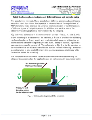
- 1. Applied Research & Photonics 470 Friendship Road, Suite 10 Harrisburg, PA 17111, USA Phone: +1-717-220-1003 http://arphotonics.net Email: info@arphotonics.net Paint thickness characterization of different layers and particle sizing Five panels were received. These panels have different primer and paint layers as well as clear over coats. The objective is to demonstrate the capabilities of ARP’s terahertz nano-scanner for accurate characterization of the thicknesses of different layers of the paint panels. In addition, the particle size of the additives was also graphically characterized by 3D imaging. Fig. 1 shows a schematic of the measurement system. The X-, Y-, and Z- axis allows scanning in 3 dimensions. In addition, a -axis is available for scanning conformal surfaces. Travel length and resolution of all axes are adjustable to accommodate different sample shapes and sizes. Samples in solid, liquid and gaseous forms may be measured. The schematic in Fig. 1 is for the samples to be scanned while the source and detection system remain stationary. However, a configuration is also available where the specimen remains stationary while the source moves for scanning. The standoff distance for both the reflected and transmitted beams may be adjusted to accommodate for application as an on line quality assurance tester. Fig. 1. Schematic diagram of the scanner. Page: 1 of 6
- 2. Applied Research & Photonics 470 Friendship Road, Suite 10 Harrisburg, PA 17111, USA Phone: +1-717-220-1003 http://arphotonics.net Email: info@arphotonics.net Fig. 2 shows the resolution of the scanner at a moderate speed. As seen from Fig. 2, the resolution is ~27 nm. A higher resolution may also be achieved, however, the current resolution is sufficient for accurate characterization of the current paint panels for different layers. For particle size characterization, resolution may be tuned down to a few nanometers. Fig. 2. Data showing the resolution of the scanning system. The noise floor is on the order of 103 counts, thus the signal is strong and clear. Paint layer thickness characterization In the following, the measured data for the individual panels are presented. The thickness modeling from the reflectance measurement has been demonstrated for one (Red panel) as an example. Similar analysis can be done for all panels. Fig. 3 shows a photograph of the sample “Red panel.” Layers 1, 2, 3, & 4 are described in Table 1. The supplied thicknesses were used as the calibration for calculating each layer’s measured thickness. However, a fine scale calibration Page: 2 of 6
- 3. Applied Research & Photonics 470 Friendship Road, Suite 10 Harrisburg, PA 17111, USA Phone: +1-717-220-1003 http://arphotonics.net Email: info@arphotonics.net of each layer of paints (or primer or overcoat, etc.) is important for a finer scale measurement. Such a scheme is is available in the commercial version of ARP’s terahertz scanner. Red Panel (contains mica flakes) Table 1. Red Panel Layer# Description Thick (µm) Cumulative (µm) 1 No label 0 0 2 Primer 15.24 15.24 3 Basecoat 16.37 31.61 4 Clear coat 64.35 95.96 4 3 2 1 102 mm 10 mm Fig. 3. Photograph of the Red Panel. Layers are marked 1, 2, 3 & 4 as described in the Table above. The arrow shows the scanning direction. Scan length is 92 mm as shown in the X scale (see Fig. 4). Page: 3 of 6
- 4. Applied Research & Photonics 470 Friendship Road, Suite 10 Harrisburg, PA 17111, USA Phone: +1-717-220-1003 http://arphotonics.net Email: info@arphotonics.net Fig. 4. Scanning traces (left Y-axis) and calculated thicknesses (right Yaxis) of different layers. The blue, red and green curves are the traces from different trials. They overlap on each other, indicating accurate reproducibility of the measurement system. The layer boundary is indicated by a sudden change in the reflectance (up and down spikes on the blue curve). The thickness was calculated based on the known thicknesses of different layers in Table 1. The spikes were excluded from thickness calculation. As seen from Fig. 4, all four layers exhibit different reflectance with clearly identifiable boundary for each layer. The final layer of paint being composed of all 4 layers, exhibit higher reflectance. Estimated average thickness of layer 4 is ~95 µm, while that of layer 3 is ~32 µm. This gives a thickness for the overcoat layer ~63 µm. Similarly, the thickness of the paint layer (layer 2) is ~16 µm. The observed fluctuation in the layer 4 thickness is not necessary indicative or measure of the paint layer roughness. This Page: 4 of 6
- 5. Applied Research & Photonics 470 Friendship Road, Suite 10 Harrisburg, PA 17111, USA Phone: +1-717-220-1003 http://arphotonics.net Email: info@arphotonics.net fluctuation may occur from several factors. However, most likely contributing factor being the surface roughness of the substrate on which the layers were deposited. As such the roughness of the substrate must be characterized before putting the primer and paint layers. Such calibration may be used as the reference for subsequent layer’s thickness measurements. Particle size characterization An attempt was made to characterize the particle size of mica flakes within the paint. Fig. 5 shows a 3D surface plot of a small area on the Red panel while Fig. 6 shows a contour plot of the same area. The surface texture in Fig. 5 is presumed due to the mica flake particles. In view of the smallest contours in Fig. 6, it may be surmised that there is size distribution of the mica particles embedded in the paint. The smallest particles may be estimated to be a few microns. A quantitative analysis may be conducted to determine the size distribution. Fig. 5. Surface plot of the Red Panel over 250 µm x 225 µm area Page: 5 of 6
- 6. Applied Research & Photonics 470 Friendship Road, Suite 10 Harrisburg, PA 17111, USA Phone: +1-717-220-1003 http://arphotonics.net Email: info@arphotonics.net Fig. 6. Contour plot of the same area as in Fig. 5. Smallest contour size may be assigned to the particle size after a size calibration is conducted. Figs. 7 through 14 respectively exhibit a photograph followed by scanning data of the rest of the 4 panels. Analyses similar to the red panel may be conducted for all of these panels. Conclusions It has been demonstrated that ARP’s terahertz nano-scanner may be used for non-destructive, non-invasive, and non-contact measurement of paint layer thicknesses and the embedded particle size estimation. The remote measurement system may be implemented for auto body paint quality inspection at the production line as well as for various paint related research and development. Contact For more information please contact: Anis Rahman, PhD Phone: 717-623-8201 Email: a.rahman@arphotonics.net Page: 6 of 6