Digital logic
•Télécharger en tant que PPTX, PDF•
1 j'aime•214 vues

Digital Logic - AND, OR, NOT, NAND, NOR Gates

Recommandé
Contenu connexe
Tendances
Tendances (20)
Similaire à Digital logic
Similaire à Digital logic (20)
Plus de Madhu Bala
Dernier
Dernier (20)
Digital logic
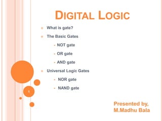
- 1. DIGITAL LOGIC What is gate? The Basic Gates NOT gate OR gate AND gate Universal Logic Gates NOR gate NAND gate 1 Presented by, M.Madhu Bala
- 2. GATES A digital circuit having one or more input signals but only one output signal is called a gate. Connecting the basic gates in different ways makes it possible to produce circuits. Gates are often called logic circuits. The basic gates can be used to produce any digital system. The three basic logic circuits are the inverter (NOT) the OR gate and the AND gate 2
- 3. THE INVERTER (NOT GATE) A NOT gate has one input signal and one output signal. The output Y of NOT gate is always complement of input A. In equation form Y= NOT A Y=A‘ Y=A There are only two possible voltage levels (low and high) associated with a digital circuit. This fits with the binary number system (0&1) This is often referred to as two-state operation. In the positive logic, the higher voltage level is assigned the binary value 1 (H=1) the lower voltage level is assigned the binary value 0 .(L=0) 3 A Y=A’ L H H L A Y=A’ 0 1 1 0 Logic Circuit of NOT gate Truth Table
- 4. THE INVERTER (NOT GATE) TTL NOT Gates Pinout diagram of a 7404 hex inverter This IC contains six inverters. After applying +5 V to pin 14 and grounding pin 7, you can connect any or all inverters to other Transistor–Transistor Logic(TTL) devices. 4
- 5. OR GATE An OR gate has two or more input signals but only one output signal. It is called an OR gate because the output voltage is high if any or all of the input voltages are high. In Boolean equation form Y = A OR B Y = A + B The '+' sign represents the logic operation OR The number of rows in a truth table equals 2n, where n is the number of inputs 5 Logic Circuit of OR gate A B Y=A+B 0 0 0 0 1 1 1 0 1 1 1 1 Truth Table
- 6. Three- input OR gate The inputs are A, B, and C. When all inputs are low, the output is low. If any input is high, the output will be high. Boolean Equation Form: Y = A+B+C 6 OR GATE (CONT..) A B C Y=A+B+C 0 0 0 0 0 0 1 1 0 1 0 1 0 1 1 1 1 0 0 1 1 0 1 1 1 1 0 1 1 1 1 1Logic Circuit of 3-input OR gate Truth Table
- 7. TTL OR Gates This digital IC contains four 2-input OR gates inside a 14- pin DIP. After connecting a supply voltage of +5 V to pin 14 and a ground to pin 7, you can connect one or more of the OR gates to other TTL devices. 7 OR GATE (CONT.)
- 8. Timing diagram for 2-input OR gate The input voltages drive pins 1 and 2 of a 7432. The output (pin 3) is low only when both inputs are low. The output is high the rest of the time. 8 OR GATE (CONT..)
- 9. The AND gate has a high output only when all inputs are high. otherwise the output will be low. AND gate also known as all-or-nothing gate. In Boolean equation form Y =A AND B Y=A.B Y=AB The '.' sign represents the logic AND operation. 9 AND GATE A B Y=AB 0 0 0 0 1 0 1 0 0 1 1 1Logic Circuit of AND gate Truth Table
- 10. Three- input AND gate The inputs are A, B, and C. When all inputs are high, the output is high. If even one input is low, the output is in the low state. In Boolean equation form: Y=A.B.C Y=ABC 10 AND GATE (CONT..) A B C Y=ABC 0 0 0 0 0 0 1 0 0 1 0 0 0 1 1 0 1 0 0 0 1 0 1 0 1 1 0 0 1 1 1 1 Logic Circuit of AND gate Truth Table
- 11. TTL AND Gates This digital IC contains four 2-input AND gates. After connecting a supply voltage of +5V to pin 14 and a ground to pin 7, you can connect one or more of the AND gates to other TTL devices. TTL AND gates are also available in triple 3-input and dual 4-input packages. 11 AND GATE (CONT..)
- 12. Timing diagram for a 2-input AND gate The input voltages drive pins 1 and 2 of a 7408. the output (pin 3) is high only when both inputs are high. The output is low the rest of the time. 12 AND GATE (CONT..)
- 13. The NAND & NOR gates are called universal gates because they can perform all the logical operations of basis gates like AND, OR, NOT. 13 Universal Logic Gate
- 14. The circuit of NOR gate is a circuit of OR gate followed by an inverter The output of NOR gate is Y=A+B NOR Gates also called a NOT-OR gate. All inputs must be low to get a high output. If any input is high, the output is low. 14 NOR GATE Logic Circuit of NOR Gates Abbreviated form Standard form IEEE form Truth Table A B Y=(A+B)’ 0 0 1 0 1 0 1 0 0 1 1 0
- 15. Pin- out Diagram of NOR gate 15 NOR GATE (CONT.)
- 16. Bubbled AND Gate Bubbled AND Gate inverters on the input lines of an AND gate. The output of bubbled AND gate and NOR gate are identical. Therefore, these two circuits are equivalent and thus interchangeable. The output of bubbled AND gate is represented as Y= A . B 16 NOR GATE (CONT.) Abbreviated form Standard form Truth Table A B A’ B’ Y=A’.B’ 0 0 1 1 1 0 1 1 0 0 1 0 0 1 0 1 1 0 0 0 Logic Circuit of Bubbled AND Gates
- 17. De Morgan's First Theorem NOR gate : Y=(A+B)’ bubbled AND gate : Y=A’B’ The outputs are equal for the same inputs, so that (A+B)’ = A’B’ The complement of a sum equals the product of the complements. This identity is known as De Morgan’s, first theorem. This can also be proved by comparing the truth tables of NOR and bubbled AND gates. Three input NOR gate and three input bubbled AND gate are identical and it can write, (A+ B + C)' = A'B'C' This equivalence can be extended to gates or circuits for larger number of inputs, too. 17 NOR GATE (CONT.)
- 18. NOT from NOR To get a NOT gate, tie inputs of NOR gate together so that there is only one input to the circuit. If input is 0, then both the inputs to NOR gate are 0 that gives output 1. Similarly, if input is 1, both the inputs to NOR gate are 1 that gives output 0. Therefore the output of circuit is complement of its input and thus gives NOT operation. 18 NOR GATE (CONT.)
- 19. OR from NOR To get a OR gate, two NOR gates are used. The first NOR gate performs usual NOR operation. The second NOR gate performs as NOT gate and inverts the NOR logic to OR 19 NOR GATE (CONT.) A+B
- 20. AND from NOR To get a AND gate, three NOR gates are used. The first and second NOR gate performs as NOT gate. NOT gates are replaced by NOR equivalent. Since NOR gate is NOT operation followed by OR we invert the output of example 2.3, shown in Fig. 2.9b to get output of this circuit. Thus output of circuit in Fig. 2.2 lc is high only when both the inputs are high and it functions like an AND gate. 20 NOR GATE (CONT.)
- 21. The circuit of NAND gate is a circuit of AND gate followed by an inverter The output of NAND gate is Y=AB "Y equals NOT A AND B" NAND Gates also called a NOT-AND gate. All inputs must be high to get a low output. If any input is low, the output is high. 21 NAND GATE Logic Circuit of NAND Gate Abbreviated form Standard form IEEE form Truth Table A B AB Y=AB 0 0 0 1 0 1 0 1 1 0 0 1 1 1 1 0
- 22. Pin- out Diagram of NAND gate 22 NAND GATE (CONT.)
- 23. Bubbled OR Gate Bubbled OR Gate inverters on the input lines of an OR gate. The output of bubbled OR gate and NAND gate are identical. Therefore, these two circuits are equivalent and thus interchangeable. The output of bubbled OR gate is represented as Y=A+B 23 NAND GATE (CONT.) A B A B Y=A+B 0 0 1 1 1 0 1 1 0 1 1 0 0 1 1 1 1 0 0 0 Abbreviated form Standard form Truth TableLogic Circuit of Bubbled OR Gate
- 24. De Morgan's Second Theorem NAND Gate :(AB)’ Bubbled OR Gate : Y=A’+B’ The outputs are equal for the same inputs, so that (AB)’ = A’+B’ The complement of a product equals the sum of the complements. This identity is known as De Morgan’s second theorem. This can also be proved by comparing the truth tables of NAND gate and bubbled OR gate. Three input NAND gate and three input bubbled OR gate are identical and it can write, (ABC)' = A’+B‘+C’ This equivalence can be extended to gates or circuits with any number of inputs. 24 NAND GATE (CONT.)
- 25. THANK YOU 25