SlideShare une entreprise Scribd logo
1  sur  104
Télécharger pour lire hors ligne
1
Ver. 1.0 2007. 06
Model Name Using Similar Mechanism NEW
CD
CD Mechanism Type CDM74KF-K6BD91UR-WOD//M
Section
Optical Pick-up Name KSM-213DCP/C2NP
Tape Deck
Model Name Using Similar Machanism HCD-GN1100D
Section
SERVICE MANUAL E Model
Australian Model
HCD-GTX88
Amplifier section
Brazil model only
The following are measured at
AC 127 V or 220 V, 50/60 Hz
Front/Surround speaker
RMS output power: 205 W + 205 W
(at 8 Ω, 1 kHz, 10% THD)
Subwoofer
RMS output power: 130 W + 130 W
(at 6 Ω, 100 Hz, 10% THD)
Other models
The following are measured at
Mexican model: AC 127 V, 60 Hz
Other models: AC 120, 220, 240 V, 50/60 Hz
Front/Surround speaker
Power Output (rated): 175 W + 175 W
(at 8 Ω, 1 kHz, 1% THD)
RMS output power (reference):
255 W + 255 W
(per channel at 8 Ω, 1 kHz,
10% THD)
Subwoofer
RMS output power (reference):
130 W + 130 W
(at 6 Ω, 100 Hz, 10% THD)
SPECIFICATIONS
Inputs
VIDEO (AUDIO IN) L/R:
Voltage 250 mV,
impedance 47 kilohms
AUDIO (AUDIO IN) L/R:
Voltage 450 mV,
impedance 47 kilohms
MIC: Sensitivity 1 mV,
impedance 10 kilohms
(USB) port: Type A
Outputs
PHONES: accepts headphones of
8 ohms or more
Disc player section
System Compact disc and digital
audio system
Laser Semiconductor laser
(λ=770 – 810 nm)
Emission duration:
continuous
Laser Output Max. 44.6 µW*
* This output is the value measured
at a distance of 200 mm from the
objective lens surface on the Optical
Pick-up Block with 7 mm aperture.
Sony Corporation
Personal Audio Division
Published by Sony Techno Create Corporation
9-887-753-01
2007F04-1
© 2007. 06
– Continued on next page –
CD DECK RECEIVER
• HCD-GTX88 is the tuner, deck,
CD and amplifier section in
MHC-GTX88.
2
HCD-GTX88
SAFETY-RELATED COMPONENT WARNING!!
COMPONENTS IDENTIFIED BY MARK 0 OR DOTTED LINE
WITH MARK 0 ON THE SCHEMATIC DIAGRAMS AND IN
THE PARTS LIST ARE CRITICAL TO SAFE OPERATION.
REPLACE THESE COMPONENTS WITH SONY PARTS WHOSE
PART NUMBERS APPEAR AS SHOWN IN THIS MANUAL OR
IN SUPPLEMENTS PUBLISHED BY SONY.
Frequency response 20 Hz – 20 kHz
Wave length 770 – 810 nm
Signal-to-noise ratio More than 90 dB
Dynamic range More than 88 dB
Tape deck section
Recording system 4-track 2-channel stereo
Frequency response 50 – 13,000 Hz (±3 dB),
using Sony TYPE I tape
Tuner section
FM stereo, FM/AM superheterodyne tuner
FM tuner section
Tuning range
Brazil model: 87.5 – 108.0 MHz
(100 kHz step)
Other models: 87.5 – 108.0 MHz
(50 kHz step)
Antenna FM lead antenna
Antenna terminals 75 ohm unbalanced
Intermediate frequency 10.7 MHz
AM tuner section
Tuning range
Latin American and Oceanian models:
530 – 1,710 kHz (with the
interval set at 10 kHz)
531 – 1,710 kHz (with the
interval set at 9 kHz)
Other models: 531 – 1,602 kHz (with the
interval set at 9 kHz)
530 – 1,610 kHz (with the
interval set at 10 kHz)
Antenna AM loop antenna
Antenna terminals External antenna terminal
Intermediate frequency 450 kHz
USB section
Supported bit rate MP3 (MPEG 1 Audio Layer 3):
32 – 320 kbps, VBR
Sampling frequencies MP3 (MPEG 1 Audio Layer 3):
32/44.1/48 kHz
Transfer speed Full-Speed
Supported USB device Mass Storage Class
Maximum current 500 mA
General
Power requirements
Mexican model: 127 V AC, 60 Hz
Brazil model: 127 V or 220 V AC, 50/60 Hz,
Adjustable with voltage
selector
Oceanian model: 230 – 240 V AC, 50/60 Hz
Argentina model: 220 V AC, 50/60 Hz
Other models: 120 V, 220 V or 230 – 240 V AC,
50/60 Hz, adjustable with
voltage selector
Power consumption 430 W
Dimensions (w/h/d) (Approx.)
281 × 361 × 417 mm
Mass (Approx.) 14.2 kg
Design and specifications are subject to change without
notice.
3
CAUTION
Use of controls or adjustments or performance of procedures
other than those specified herein may result in hazardous
radiation exposure.
HCD-GTX88
NOTES ON HANDLING THE OPTICAL PICK-UP BLOCK
OR BASE UNIT
The laser diode in the optical pick-up block may suffer electrostatic
breakdown because of the potential difference generated by the
charged electrostatic load, etc. on clothing and the human body.
During repair, pay attention to electrostatic break-down and also
use the procedure in the printed matter which is included in the
repair parts.
The flexible board is easily damaged and should be handled with
care.
Notes on Chip Component Replacement
• Never reuse a disconnected chip component.
• Notice that the minus side of a tantalum capacitor may be
damaged by heat.
Flexible Circuit Board Repairing
• Keep the temperature of soldering iron around 270°C during
repairing.
• Do not touch the soldering iron on the same conductor of the
circuit board (within 3 times).
• Be careful not to apply force on the conductor when soldering
or unsoldering.
UNLEADED SOLDER
Boards requiring use of unleaded solder are printed with the lead
free mark (LF) indicating the solder contains no lead.
(Caution: Some printed circuit boards may not come printed with
the lead free mark due to their particular size)
: LEAD FREE MARK
Unleaded solder has the following characteristics.
• Unleaded solder melts at a temperature about 40 °C higher than
ordinary solder.
Ordinary soldering irons can be used but the iron tip has to be
applied to the solder joint for a slightly longer time.
Soldering irons using a temperature regulator should be set to about
350 °C.
Caution: The printed pattern (copper foil) may peel away if the
heated tip is applied for too long, so be careful!
• Strong viscosity
Unleaded solder is more viscou-s (sticky, less prone to flow) than
ordinary solder so use caution not to let solder bridges occur such
as on IC pins, etc.
• Usable with ordinary solder
It is best to use only unleaded solder but unleaded solder may also
be added to ordinary solder.
This appliance is
claassified as a CLASS 1
LASER product. This
label is located on the
rear exterior.
NOTES ON LASER DIODE EMISSION CHECK
The laser beam on this model is concentrated so as to be focused on
the disc reflective surface by the objective lens in the optical pick-
up block. Therefore, when checking the laser diode emission,
observe from more than 30 cm away from the objective lens.
Laser component in this product is capable
of emitting radiation exceeding the limit for
Class 1.
4
HCD-GTX88
MODEL IDENTIFICATION
– MODEL NUMBER LABEL –
MODEL PARTS No.
GTX88: E2 3-113-126-0s
GTX88: E51 3-198-009-0s
GTX88: AUS 3-197-997-0s
GTX88: AR 3-198-001-0s
• Abbreviation
E2 : 120V AC area in E model
E51 : Chilean and Peruvian model
AR : Argentina model
AUS : Australian model
PART No.
5
TABLE OF CONTENTS
HCD-GTX88
1. GENERAL
Guide to parts and controls ...................................................... 6
2. DISASSEMBLY
2-1. Case (Top) ......................................................................... 13
2-2. Loading Panel.................................................................... 13
2-3. Tuner Pack ......................................................................... 14
2-4. CD Block Section.............................................................. 14
2-5. Front Panel Section ........................................................... 15
2-6. Tape Mechanism Deck, Mic Board,
USB Connector Board ....................................................... 15
2-7. Panel Board, Function Board, Jog Board .......................... 16
2-8. CD-SW Board ................................................................... 16
2-9. Cover (CDM) .................................................................... 17
2-10. Back Panel Section ............................................................ 17
2-11. Power Board Section ......................................................... 18
2-12. Main Board ....................................................................... 18
2-13. Subwoofer Board, Power Board........................................ 19
2-14. Power Transformer (T1200) .............................................. 19
2-15. BD91 Board ...................................................................... 20
2-16. Driver Board, SW Board, USB Board .............................. 20
2-17. Optical Pick-up ................................................................. 21
2-18. Sensor Board ..................................................................... 21
2-19. Motor (TB) Board ............................................................. 22
2-20. Motor (LD) Board ............................................................. 22
3. TEST MODE ..................................................................... 23
4. MECHANICAL ADJUSTMENTS ............................... 27
5. ELECTRICAL ADJUSTMENTS................................. 28
6. DIAGRAMS
6-1. Block Diagram — RF/Servo Section — ........................... 31
6-2. Block Diagram — Tape/Tuner Section — ........................ 32
6-3. Block Diagram — Main Section — .................................. 33
6-4. Block Diagram — USB Section — .................................. 34
6-5. Block Diagram — AMP/Subwoofer Section — ............... 35
6-6. Block Diagram — Display/Power Section — .................. 36
6-7. Circuit Boards Location .................................................... 37
6-8. Printed Wiring Board — BD91 Section — ....................... 40
6-9. Schematic Diagram — BD91 Section —.......................... 41
6-10. Printed Wiring Boards — Driver Section —..................... 42
6-11. Schematic Diagram — Driver Section — ......................... 43
6-12. Schematic Diagram — Main Section (1/4) — .................. 44
6-13. Schematic Diagram — Main Section (2/4) — .................. 45
6-14. Schematic Diagram — Main Section (3/4) — .................. 46
6-15. Schematic Diagram — Main Section (4/4) — .................. 47
6-16. Printed Wiring Board — Main Section — ........................ 48
6-17. Printed Wiring Board — USB Connector Section — ....... 49
6-18. Schematic Diagram — USB Connector Section — .......... 49
6-19. Printed Wiring Board — USB Section —......................... 50
6-20. Schematic Diagram — USB Section — ........................... 51
6-21. Printed Wiring Board — Effector Section — ................... 52
6-22. Schematic Diagram — Effector Section — ...................... 53
6-23. Printed Wiring Board — Panel Section —........................ 54
6-24. Schematic Diagram — Panel Section — .......................... 55
6-25. Printed Wiring Boards — Function Section —................. 56
6-26. Schematic Diagram — Function Section — ..................... 57
6-27. Printed Wiring Board — Power Amp Section — ............. 58
6-28. Schematic Diagram — Power Amp Section — ................ 59
6-29. Printed Wiring Board — Subwoofer Section — ............... 60
6-30. Schematic Diagram — Subwoofer Section —.................. 61
6-31. Printed Wiring Boards — Trans Section — ...................... 62
6-32. Schematic Diagram — Trans Section — .......................... 63
7. EXPLODED VIEWS
7-1. Main Section ..................................................................... 78
7-2. Front Panel Section (1)...................................................... 79
7-3. Front Panel Section (2)...................................................... 80
7-4. Front Panel Section (3)...................................................... 81
7-5. Chassis Section ................................................................. 82
7-6. CD Mechanism Section (1) ............................................... 83
7-7. CD Mechanism Section (2) ............................................... 84
8. ELECTRICAL PARTS LIST ........................................ 85
6
HCD-GTX88
SECTION 1
GENERAL This section is extracted
from instruction manual.
6GB
Guide to parts and controls
This manual mainly explains operations using the buttons on the unit, but the same
operations can also be performed using the buttons on the remote having the same or
similar names.
Unit
– Front view
– Top view
qdqfqgqh
1 2 3 4
5
6
qj
qk
ql
w;
wa
ws
wd
wf
7
8
9
q;
qa
qs
wkwj wgwh
7
HCD-GTX88
7GB
Guidetopartsandcontrols
1 FLANGER (pages 35, 43, 48)
DELAY (pages 35, 43, 48)
CHORUS (pages 36, 43, 48)
SOUND FLASH (page 35)
Press to create a party atmosphere.
B Display (pages 9, 38, 39, 48)
C SURROUND SPEAKER MODE
(MHC-GTX88 only) (page 34)
Press to select the sound system.
SURROUND
(MHC-GTX77/MHC-GTX66 only)
(page 34)
Press to select the surround effect.
D Disc tray (pages 9, 17, 44, 48)
E AMP MENU (page 38)
Press to change the spectrum
analyser display or to adjust the
brightness of the display.
F RETURN (pages 17, 25)
Press to return to the parent folder.
G NX (play/pause) (pages 17, 22,
24, 30, 44)
Press to start or pause playback.
x (stop) (pages 17, 23, 25, 28,
29, 30, 32, 44)
Press to stop playback or recording.
./> (go forward/go
backward) (pages 17, 20, 23, 25,
27, 31, 48)
Press to select a track.
TUNING +/– (pages 28, 29)
Press to tune in a radio station.
+/– (pages 17, 20, 23, 25, 27,
31)
Press to select a folder.
m/M (rewind/fast forward)
(page 30)
Press to fast forward or rewind.
H CD- SYNC/REC 1 (page 22)
Press to record from a disc onto the
connected optional USB device
(Digital music player or USB storage
media).
CD-TAPE SYNC (page 31)
TAPE REC PAUSE/START
(page 31)
Press to record onto a tape.
I PUSH OPEN/CLOSE Z (Deck B)
(page 30)
Press to insert or eject a tape.
Deck B (pages 30, 31, 37, 48)
J ENTER (pages 23, 29, 33, 48)
Press to enter the selection.
K ERASE (page 23)
Press to erase MP3 audio tracks or
folders on the connected optional
USB device (Digital music player or
USB storage media).
L MASTER VOLUME (pages 17,
24, 39, 43)
Turn to adjust the volume.
M MIC (jack) (pages 36, 43, 52)
Connect an optional microphone.
MIC LEVEL (pages 32, 36, 43)
Turn to adjust the microphone
volume.
USB
Continued l
8
HCD-GTX88
8GB
N REC/ERASE (indicator)
(pages 23, 25)
Lights up when recording from a disc
onto the connected optional USB
device (Digital music player or USB
storage media).
Lights up when erasing MP3 audio
tracks from the connected optional
USB device (Digital music player or
USB storage media).
O (USB) port (pages 22, 23,
24, 41, 52)
Connect an optional USB device
(Digital music player or USB storage
media).
P PHONES (jack) (pages 43, 52)
Connect the headphones.
Q Power illuminator (pages 35, 39)
R PRESET EQ (page 33)
Press to select a preset sound effect.
S Z PUSH OPEN/CLOSE (Deck A)
(page 30)
Press to insert or eject a tape.
Deck A (pages 30, 48)
T Function buttons:
CD (pages 14, 17, 22, 29, 31, 38)
TUNER/BAND (pages 29, 38)
TAPE A/B (pages 30, 38)
AUDIO (pages 38, 41)
VIDEO (pages 38, 41)
(pages 23, 24, 26, 38)
Press to select a function.
U "/1 (on/standby) (pages 13, 14,
29, 43, 48)
Press to turn the system on or off.
V GROOVE (page 33)
Press to reinforce the bass.
W IR Receptor (page 43)
X EQ BAND/MEMORY (page 33)
Press to select a frequency band
when adjusting the graphic
equalizer.
Y DISPLAY (pages 38, 39, 40)
Press to change the information in
the display.
Z OPERATION DIAL (pages 17,
25, 33, 35, 38)
Turn to select a track or folder.
Turn to select a setting.
wj ILLUMINATION (page 39)
Press to change the power
illuminator pattern.
wk DISC SKIP/EX-CHANGE
(pages 14, 17, 18, 20)
Press to skip a disc.
Press to exchange other discs during
playback.
Z OPEN/CLOSE (pages 14, 17,
44)
Press to load or eject a disc.
DISC 1 ~ 3 (pages 18, 20)
Press to select a disc.
Press to switch to CD function from
other function.
USB
9
HCD-GTX88
9GB
Guidetopartsandcontrols
– Display
A Lights up when the USB function is
selected (page 24).
B “MP3” lights up when an MP3 audio
track is recognized. “CD” lights up
when a disc is recognized.
C Indicates the type of MP3 audio track
information that displayed (page 39).
“ ” lights up when a track name is
displayed. “ ” lights up when an
artist name is displayed. “ ” lights
up when a folder name is displayed.
D Indicates the tuner band (page 28).
E Lights up when the MP3 audio track
contains ID3 tag information.
F Displays the current status and
information (page 39).
G Indicators for the TUNER function
(page 28).
H Lights up when the Play Timer or
Recording Timer is set (page 37).
I Lights up when the Sleep Timer is
activated (page 37).
J Lights up during recording (pages 22,
31).
K Indicators for the TAPE function
(page 30).
“ ” and “ ” lights up when the
system is turned on.
“ ” lights up when there is a tape in
the deck.
L Lights up when an optional USB
device (Digital music player or USB
storage media) is recognized
(page 22).
M Indicates the selected play mode
(pages 19, 26).
N Indicators for the disc tray (page 17).
“ ” lights up when the disc is
selected. “ ” lights up when there is
a disc on the disc tray. “1”, “2” and
“3” light up when the system is turned
on.
O Indicates the activated sound effect
(pages 33, 35).
Note
“LINK”, “MATRIX SUR 1” and
“MATRIX SUR 2” light up for
MHC-GTX88 only.
FM AM ID3 AUTO PRESET ST
MONO
MHz
kHz
TUNED
REC
PLAY
SLEEP
CD
USB
MP3 BOOSTER
SUR
FLANGER CHORUS DELAY
MATRIX SUR 12
LINK
Z GROOVE
SHUF TAPE USB
USB MEMORY
PGM
ALL 1 DISCS
REP 1
SYNC
A B1 2 3
qa q;qs
432 5 6 7 81
9qdqfqg
MP3
REC
A B
Continued l
10
HCD-GTX88
10GB
Subwoofer A (SS-WG88A)
1 SUBWOOFER ON/OFF
(page 13)
Press to turn the subwoofer on or off.
2 SUBWOOFER LEVEL (page 13)
Turn to adjust the subwoofer level.
Remote
1 "/1 (on/standby) (pages 13, 16,
43)
Press to turn the system on or off.
B CLOCK/TIMER SELECT
(page 38)
CLOCK/TIMER SET (pages 16,
37)
Press to set the clock and the timers.
C REPEAT/FM MODE (pages 21,
27, 29, 47)
Press to change the Repeat Play
setting.
Press to select the FM monaural or
stereo reception.
D USB (page 24)
Press to select the USB function.
CD (page 17)
Press to select the CD function.
TUNER/BAND (page 28)
Press to select the TUNER function.
Press to select FM or AM band.
FUNCTION (pages 30, 41)
Press to select a function.
2
1
q;
qa
qs
qd 3
4
5
2
6
7
9
8
qf
1qg
11
HCD-GTX88
11GB
Guidetopartsandcontrols
E ./> (go forward/go
backward) (pages 17, 20, 23, 25,
27, 31, 37, 48)
Press to select a track.
+/– (tuning) (pages 28, 29)
Press to tune in a radio station.
m/M (rewind/fast forward)
(pages 17, 25, 30)
Press to find a point in a track.
(play) (pages 17, 24, 30, 44)
X (pause) (pages 17, 30)
x (stop) (pages 17, 25, 28, 30,
32)
Press to start, pause or stop playback.
F ENTER (pages 16, 23, 28, 33,
37)
Press to enter the selection.
G DISC SKIP (pages 18, 20)
Press to skip a disc.
H +/– (pages 17, 20, 23, 25, 27,
31)
Press to select a folder.
I VOLUME +/–* (pages 17, 24, 39,
43)
Press to adjust the volume.
* The VOLUME + button has a tactile dot.
Use the tactile dot as a reference when
operating the system.
J EQ (page 33)
Press to select a preset sound effect.
K CLEAR (pages 21, 27)
Press to delete a pre-programmed
track.
L PLAY MODE/TUNING MODE
(pages 19, 26, 28, 29, 44)
Press to select the play mode of CD
or USB function.
Press to select the tuning mode.
qd TUNER MEMORY (page 28)
Press to preset a radio station.
qf DISPLAY (pages 38, 39, 40)
Press to change the information on
the display.
qg SLEEP (page 37)
Press to activate the Sleep Timer.
12
HCD-GTX88
SECTION 2
DISASSEMBLY
Note : Disassemble the unit in the order as shown below.
2-19. MOTOR (TB) BOARD
(Page 22)
2-20. MOTOR (LD) BOARD
(Page 22)
2-1. CASE (TOP)
(Page 13)
2-2. LOADING PANEL
(Page 13)
SET
2-3. TUNER PACK
(Page 14)
2-16. DRIVER BOARD,
SW BOARD,
USB BOARD
(Page 20)
2-15. BD91 BOARD
(Page 20)
2-17. OPTICAL PICK-UP
(Page 21)
2-4. CD BLOCK SECTION
(Page 14)
2-10. BACK PANEL SECTION
(Page 17)
2-5. FRONT PANEL SECTION
(Page 15)
2-18. SENSOR BOARD
(Page 21)
2-9. COVER (CDM)
(Page 17)
2-11. POWER BOARD SECTION
(Page 18)
2-13. SUBWOOFER BOARD,
POWER BOARD
(Page 19)
2-14. POWER TRANSFORMER
(T1200)
(Page 19)
2-12. MAIN BOARD
(Page 18)
2-6. TAPE MECHANISM DECK,
MIC BOARD,
USB CONNECTOR BOARD
(Page 15)
2-8. CD-SW BOARD
(Page 16)
2-7. PANEL BOARD,
FUNCTION BOARD,
JOG BOARD
(Page 16)
13
HCD-GTX88
2-2. LOADING PANEL
Note : Follow the disassembly procedure in the numerical order given.
2-1. CASE (TOP)
1 screw
(case 3 TP2)
6 screw
(case 3 TP2)
2 two screws
(case 3 TP2)
7 two screws
(case 3 TP2)
4
9
qs
3 two screws
(+BVTP 3 × 10)
8 two screws
(+BVTP 3 × 10) qa two screws
(+BVTP 3 × 10)
qd case (top)
5 panel (side-R)
0 panel (side-L)
3 loading panel
2 Pull-out the disc tray.
1 Turn the pulley to the direction of the arrow.
pulley
Front panel side
CD mechanism deck (CDM74KF)
14
HCD-GTX88
2-3. TUNER PACK
2-4. CD BLOCK SECTION
3 tuner pack
2 wire (flat type) (9 core)
(CN1)
1 two screws
(+BVTP 3 × 8)
1 screw
(+BVTP 3 × 8)
5 three screws
(+BVTP 3 × 12)
2 lug
3 tapping screw
4 tapping screw
6 wire (flat type) (13 core)
(CN701)
qs CD block section
7
9 wire (flat type) (21 core)
(CN5053)
0 CN903 (5P)
qa CN901 (2P)
8 wire (flat type) (27 core)
(CN5051)
15
HCD-GTX88
2-6. TAPE MECHANISM DECK, MIC BOARD, USB CONNECTOR BOARD
2-5. FRONT PANEL SECTION
0 front panel section
3
2 three screws
(+BVTP 3 × 8)1 three screws
(+BVTP 3 × 8)
4 wire (flat type) (17 core)
(CN508)
5 wire (flat type) (11 core)
(CN509)
7 CN503 (3P)
8 CN507 (8P)
9 CN903 (3P)
6 CN100 (4P)
1 three screws
(+BVTP 2.6 (3CR))
2 three screws
(+BVTP 2.6 (3CR))
5 two screws
(+BVTP 2.6 (3CR))
7 two screws
(+BVTP 2.6 (3CR))
9 two screws
(+BVTP 2.6 (3CR))
0 USB CONNECTOR board
bracket (MIC shield)
8 MIC board
6
3 tape mechanism deck
4 knob (MIC)
16
HCD-GTX88
2-7. PANEL BOARD, FUNCTION BOARD, JOG BOARD
2-8. CD-SW BOARD
2 two screws
(+BVTP 2.6 (3CR))
3 two screws
(+BVTP 2.6 (3CR))
8 five screws
(+BVTP 2.6 (3CR))
9 four screws
(+BVTP 2.6 (3CR))
0 six screws
(+BVTP 2.6 (3CR))
qj three screws
(+BVTP 2.6 (3CR))
4 PANEL board
qa PANEL board
qs knob (volume)
qd nut
qf holder (jog)
qg knob jog assy
qh gear (encoder)
qk JOG board
1 CN956 (2P) 6 CN905 (2P)
7 CN904 (3P)
5 wire (flat type) (25 core)
(CN900)
2
1 two screws
(+BVTP 2.6 (3CR))
3 two screws
(+BTTP (M2.6))
4 three screws
(+BTTP (M2.6))
5 CD-SW board
6 escucheon (CD)
17
HCD-GTX88
2-10. BACK PANEL SECTION
2-9. COVER (CDM)
1 two screws
(+BVTP 3 × 10)
3 cover (CDM)
CD mechanism deck
2 screw
(+BVTP 3 × 10)
5 four screws
(+BVTP 3 × 10)
7 two screws
(+BVTP 3 × 10)
8 three screws
(+BVTP 3 × 10)
6 two screws
(+BVTP 3 × 10)
4 wire (flat type) (17 core)
(CN1502)
1 CN1200 (3P)
2 CN1204 (4P)
3 CN1202 (2P)
9 CN580 (3P)
0 back panel section
18
HCD-GTX88
2-11. POWER BOARD SECTION
2-12. MAIN BOARD
2 two screws
(+BV3 (3-CR))
7 two screws
(+BV3 (3-CR))
8 screw
(+BV3 (3-CR))
9 screw
(+BV3 (3-CR))
3 DC fan(M892)
6 three screws
(+BVTP 3 × 10)
0 two screws
(+BVTP 3 × 10)
qa POWER board section
1 CN581 (3P)
4 CN1214 (6P)
5 CN1212 (7P)
1 screw
(+BVTP 3 × 10)
2 MAIN board
POWER board assy
CN600
CN601
CN700
19
HCD-GTX88
2-14. POWER TRANSFORMER (T1200)
2-13. SUBWOOFER BOARD, POWER BOARD
1 two screws
(transistor)
9 two screws
(transistor)
qd screw
(+BVTP 3 × 10)
qf bracket
qg POWER board
qs heat sink assy
6 two screws
(+BVTP 3 × 8)
7 holder
2 two screws
(+BVTP 3 × 10)
8 two screws
(+BVTP 3 × 10)0 two screws
(+BVTP 3 × 10)
qa
5 CN607 (5P)
4 SUBWOOFER board
3 screw
(+BV3 (3-CR))
2 two screws
(+BV3 (3-CR))
7 three screws
8 power transfomer (T1200)
TRANS board
6 three screws
3 DC fan(M892)
4 CN1214 (6P)
5 CN1212 (7P)
1 CN581 (3P)
20
HCD-GTX88
2-15. BD91 BOARD
2-16. DRIVER BOARD, SW BOARD, USB BOARD
3 BD91 board
2 Remove the four solders.
1 wire (flat type) (16 core)
(CN301)
2 CN703 (4P)
3 CN704 (2P)
5 DRIVER board
7 SW board
1 two screws
(+BVTT (M2.6))
6 screw
(+BVTT (M2.6))
8 two screws
(+BVTP2.6 (3CR))
9 USB board
4 wire (flat type) (5 core)
(CN702)
21
HCD-GTX88
2-17. OPTICAL PICK-UP
2-18. SENSOR BOARD
3 two coil springs
(insulator)5 two coil springs
(insulator)
4 two insulators
6 two insulators
7 optical pick-up
(BU-K6BD91UR)
1 two floating screws
(+PTPWH M2.6)
2 two floating screws
(+PTPWH M2.6)
2 tray
3 belt (table)
5 pulley (table)
8 screw
(+BTTP (M2.6))
0 SENSOR board
7 gear (geneva)
9 CN731
(3P)
1 floating screw
(+PTPWH M2.6)
6 floating screw
(+PTPWH M2.6)
4 floating screw
(+PTPWH M2.6)
22
HCD-GTX88
2-19. MOTOR (TB) BOARD
2-20. MOTOR (LD) BOARD
6 Remove the two solderings of motor.
8 MOTOR (TB) board
7 table motor assy (M741)
5 two screws
(+BTTP (M2.6))
4
1 stopper
2 stopper
table
3 wire (flat type) (5 core)
(CN742)
2 Remove the two solderings of motor.
4 MOTOR (LD) board
1 belt (loading)
5 loading motor assy (M751)
3 two screws
(+BTTP (M2.6))
23
HCD-GTX88
SECTION 3
TEST MODE
4. When the [MASTER VOLUME] knob is turned clockwise even
slightly, the sound volume increases to its maximum and a
message “VOLUME MAX” appears on the fluorescent indicator
tube.
5. When the [MASTER VOLUME] knob is turned counter-clockwise
even slightly, the sound volume decreases to its minimum and a
message “VOLUME MIN” appears on the fluorescent indicator
tube.
* Tape function
1. Insert a tape in dack B. The function is changed to VIDEO
automatically when the recording is started by pressing [CD-
TAPE SYNC] then press [TAPE REC PAUSE/START] button.
During recording theALC (Automatic Logic Control) is turned
on.
2. During recording, press m button will stop the recording
and the function is changed to TAPE B and rewind the tape in
Deck B until the recording start position and playback of the
tape in Deck B is started. If the [TAPE REC PAUSE/ START]
button is pressed for a pause and pressed again to resume
recording during recording time, when the tape is rewind, the
tape will be rewind until the position where the pause is applied.
* To release from MC Test mode
1. To release from this mode, press ?/1 button.
2. The cold reset is enforced at the same time.
[COLD RESET]
• The cold reset clears all data including preset data stored in the
RAM to initial conditions. Execute this mode when returning
the set to the customer.
Procedure:
1. Press ?/1 button to turn on the system.
2. Press x button, [ENTER] button and ?/1 button
simultaneously.
3. The message “COLD RESET” appears on the fluorescent
indicator tube. Then, the fluorescent indicator tube becomes
blank for while, and the set is reset.
[VACS ON/OFF]
• This mode is used to switch ON and OFF the VACS (Variable
Attenuation Control System).
Procedure:
1. Press ?/1 button to turn on the system.
2. Press x button and [ILLUMINATION] button simultaneously.
The message “VACS OFF” or “VACS ON” appears on the
fluorescent indicator tube.
[TUNER STEP CHANGE]
• The step interval of AM channels can be toggled between 9 kHz
and 10 kHz.
This mode is not available for Saudi Arabia model.
Procedure:
1. Press ?/1 button to turn on the system.
2. Press [TUNER/BAND] button repeatedly to select the “AM”.
3. Press ?/1 button to turn off the system.
4. Press [ENTER] button and ?/1 button simultaneously. The
system will turn on automatically. The message “AM 9K STEP”
or “AM 10K STEP” appears on the fluorescent indicator tube
and thus the channel step is changed.
[GC TEST MODE]
• This mode is used to check the fluorescent indicator tube, LEDs,
buttons, MASTER VOLUME knob, OPERATION DIAL knob,
model, destination, software version.
Procedure:
1. Press x button, [ENTER] button and [DISC 2] button
simultaneously.
2. All LEDs and segments in fluorescent indicator tube are lighted
up.
All LEDs are lighted up in red color except for NX LED
where the LED is lighted up in green color.
3. When you want to enter to the model version and destination
display mode, press [DISC 1] button. The model information
appears on the fluorescent indicator tube.
4. Each time [DISC 1] button is pressed, the display changes to
display software version and date of the software creation. The
sequence is MC version, GC version, SYS version, CD version,
CDDM version, CDMA version, CDMB version, BDA version,
BDB version, ST version, TC version, TA version, TM version,
MM1 version and MM2 version in this order, and returns to the
model version display.
5. Press [DISC 2] button, the key check mode is activated.
6. In the key check mode, the fluorescent indicator tube displays
“K 0 J0 V0”.
Turn the [OPERATIONAL DIAL] clockwise; “J” value increases
by one. Turn the [OPERATIONAL DIAL] counterclockwise; “J”
value decreases by one. Each time a button is pressed, “K” value
increases. Press other keys on main unit to check whether the
key is detected. However, once a button has been pressed, it is
no longer taken into account.
“V” value increases in the manner of 0, 1, 2, 3 ... if [MASTER
VOLUME] knob is turned clockwise, or it decreases in the manner
of 0, 9, 8, 7 ... if [MASTER VOLUME] knob is turned
counterclockwise.
7. When [DISC SKIP/EX-CHANGE] button is pressed after all LEDs
and segments in fluorescent indicator tube light up, alternate
segments in fluorescent indicator tube and LED would light up.
If you press [DISC SKIP/EX-CHANGE] button again, another half
of alternate segments in fluorescent indicator tube and LEDs
would light up. Pressing [DISC SKIP/EX-CHANGE] button again
would cause all LED and segments lights up.
8. To release from this mode, press three buttons in the same
manner as step 1, or disconnect the power cord.
[MC TEST MODE]
• This mode is used to check operations of the respective sections
of Amplifier, Tuner and Tape.
Procedure:
• To enter MC Test Mode
1. Press x button, [ENTER] button and [DISC 3] button
simultaneously.
2. The CD ring indicators and TAPE A and B indicators flash on
the fluorescent indicator tube. The function is changed to
VIDEO.
* Check of Amplifier
1. Press [EQ BAND/MEMORY] button repeatedly until a message
“GEQ MAX” appears on the fluorescent indicator tube. GEQ
increases to its maximum.
2. Press [EQ BAND/MEMORY] button repeatedly until a message
“GEQ MIN” appears on the fluorescent indicator tube. GEQ
decreases to its minimum.
3. Press [EQ BAND/MEMORY] button repeatedly until a message
“GEQ FLAT” appears on the fluorescent indicator tube. GEQ
is set to flat.
24
HCD-GTX88
[CD SERVICE MODE]
• This mode let you move the CD sled motor freely. Use this mode
when you want to clean the optical pick-up.
Procedure:
1. Press ?/1 button to turn on the system.
2. Select CD function.
3. Press x button, [ENTER] button and [OPEN/CLOSE] button
simultaneously.
4. The CD service mode is activated. The message “SERVICE
MODE” appears on the fluorescent indicator tube.
5. With the CD in stop status, press M to move the optical
pick-up to outside track, or turn m to move to inside track.
The message “SLED OUT” or “SLED IN” appears on the
fluorescent indicator tube.
6. To turn on or off the laser, press [FLANGER] button. The message
“LD ON” or “LD OFF” appears on the fluorescent indicator
tube.
7. To release from this mode, press ?/1 button to turn off the
system.
[CD AGING MODE]
• This mode can be used for operation check of CD section. If an
error occurs, the aging operation would stops and the status is
displayed. If there were no error occurs, the aging operation
would continue repeatedly.
Procedure:
1. Press ?/1 button to turn on the system.
2. Select CD function.
3. Load three discs on disc tray.
4. Press [PLAY MODE/TUNING MODE] button on the remote control
repeatedly to select the “ALL DISCS” mode, and press the
[REPEAT/FM MODE] button on the remode control repeatedly
to select repeat mode off.
5. Press x button, [ENTER] button and [DISC SKIP/EX-CHANGE]
button simultaneously.
6. Aging operation is started.
7. To release from this mode, press ?/1 button or disconnect the
power cord to turn the power OFF.
• Aging mode sequence:
DISC CHUCKING
TOC READING
PLAY FIRST TRACK FOR 2
SECONDS
OPEN THE DISC TRAY
DISC SKIP
CLOSE THE DISC TRAY
START
PLAY LAST TRACK FOR 2
SECONDS
EX-CHANGE OPEN/CLOSE
CHANGE THE NEXT DISC
25
HCD-GTX88
[CD ERROR CODE MODE]
• Display the CD error code when an error occurred.
Procedure:
1. Press x button, [ENTER] button and [DISC 1] button
simultaneously to enter the error code display mode.
2. The fluorescent indicator tube display the number of total error.
3. Each time m button and M button are turned, display
change as below.
%% : The process when trouble occurs
01 : Process ejecting DISC
02 : Process waiting for inserting DISC
03 : Process sending request to insert a disc to upper
layer.
04 : Process sending request to eject a disc to upper
layer.
05 : Process pulling a DISC in.
06 : Chucking process
07 : Re-chucking process
08 : Process cancelling chucking
&& : The operation when trouble occurs
00 : Waiting for operation.
10/11/12/13: During eject operation
20 : While pulling a disc in
30 : While cancelling chucking
40/41/42/43: During eject operation due to error.
0000 : Not used (Value is fixed to 0000).
• Display of BD error. It is shown with “D” and 11 digits
number.
DISPLAY OF
TOTAL ERROR
DISPLAY OF
MECHANICAL
ERRORS
BUTTONM m BUTTON
DISPLAY OF
NO DISC
ERRORS
BUTTONM m BUTTON
M
M
M
M
4. To clear the error record, operate the cold reset. (Refer to the
“MC COLD RESET”.)
5. To release from this mode, press the ?/1 button or disconnect
the power OFF.
• Display of total error
Em** : The number of times for CDM (mechanical) errors.
Ed** : The number of times for BD error (after chucking the
disc.).
• Display of CDM (mechanical) error. It is show with “M” and
11 digit number.
Em**Ed**
M*$$%%&&0–
000
M* : The number of history error for mechanical. (“0” is
latest one) (Turn > button to display next error.)
$$ : Mechanical errors occur in the operation.
FF : Mechanical error during normal operation.
Other: Mechanical error during initializing operation.
D*$$%%&&#–
#00
D* : The number of error history (“0” is latest one)
(Press > button to display next error.)
$$ : The detail of trouble
01 : Can not focus
02 : GFS error
03 : Start-up time over
04 : Continuously out of focus
05 : Q code is not input for certain time
06 : Tracking on is impossible
07 : Blank disc
%% : The process when trouble occurs
01 : While SHIP process is performed
02 : While POWER OFF is processed
03 : While INITIALIZE (POWER ON) is processed.
04 : While oscillation stops
05 : From stopping oscillation to start oscillation
06 : During stop
07 : During STOP operation
08 : While start-up is processed
09 : While TOC reading is processed
0a : During search operation
0b : During PLAY operation
0c : During pause operation
0d : During PLAY manual search operation
0e : During PAUSE manual search operation
&& : Processing operation when trouble occurs
Show each STEP mentioned in %% digits.
## : Disc speed when trouble occurs.
01 : x1 speed
02 : x2 speed (for models which support x2 speed)
04 : x4 speed
00 : Not used (value is fixed to 00).
26
HCD-GTX88
[CD REPEAT 5 LIMIT OFF MODE]
• The number of repeat for CD playback is 5 times when the re-
peat mode is “REPEAT ALL”. This mode enables CD to repeat
playback for limitless times.
Procedure:
1. Press ?/1 button to turn on the system.
2. Select CD function.
3. Press x button, [CD] button and [DISC 1] button simultaneously
to enter the CD repeat 5 limit off mode and the fluorescent
indicator tube displays “LIMIT OFF”.
• To release from this mode, operate the cold reset.
(Refer to the “MC COLD RESET”.)
[CD SHIP MODE (WITH MEMORY CLEAR)]
• This mode moves the optical pick-up to the position durable to
vibration and clears all data including preset data stored in the
RAM to initial conditions. Use this mode when returning the set
to the customer after repair.
Procedure:
1. Press ?/1 button to turn on the system.
2. Select CD function.
3. Press x button, [SOUND FLASH] button and ?/1 button
simultaneously. The system will turn off automatically.
4. After the “STANDBY” blinking display finishes, a message
“MECHA LOCK” is displayed on the fluorescent indicator tube
and the CD ship mode is set.
5. The Memory is clear after AC Power OFF.
[CD SHIP MODE (WITHOUT MEMORY CLEAR)]
• This mode moves the optical pick-up to the position durable to
vibration. Use this mode when returning the set to the customer
after repair.
Procedure:
1. Press ?/1 button to turn on the system.
2. Select CD function.
3. Press [CD] button and ?/1 button button simultaneously. The
system will turn off automatically.
4. After the “STANDBY” blinking display finishes, a message
“MECHA LOCK” is displayed on the fluorescent indicator tube
and the CD ship mode is set.
[CD/USB POWER MANAGE]
• This mode let you switch on or off power supply to the BU and
USB Micom during TUNER function.
• When CD and USB POWER is set to OFF, the power supply to
the BU and USB Micom is cut off during TUNER function. It
will increase the time taken to access CD and USB when function
change from TUNER to CD or USB but it will improve tuner
reception.
• When CD and USB POWER is set to ON, the power supply to
the BU and USB Micom is not cut off during TUNER function.
It will reduce the time taken to access CD or USB when function
change from TUNER to CD or USB but it will decrease tuner
reception performance.
Procedure:
1. Press ?/1 button to turn on the system.
2. Select CD section.
3. Press ?/1 button to turn off the system.
4. When demonstration appear, press x button and ?/1 button
simultaneously. The set will power on automatically.
5. The message “CD/USB POWER ON” or “CD/USB POWER
OFF” will be displayed on the fluorescent indicator tube.
[CD TRAY LOCK MODE]
• This mode let you lock the disc tray.When this mode is activated,
the disc tray will not open when [OPEN/CLOSE] button or [DISC
SKIP/EX-CHANGE] button is pressed. The message “LOCKED”
will be displayed on the fluorescent indicator tube.
Procedure:
1. Press ?/1 button to turn on the system.
2. Select CD function.
3. Press x button, [OPEN/CLOSE] button simultaneously and
hold down until “LOCKED” or “UNLOCKED” displayed on
the fluorescent indicator tube (around 5 seconds).
[TCM OFFLINE MODE]
• This mode is used to prevent the system from turning off auto-
matically when TCM is not connected. Therefore, measurements
can be done even when TCM is not connected during produc-
tion.
Procedure:
1. When the system is turned off, press [EQ BAND/MEMORY]
button, [TAPE A/B] button and ?/1 button simultaneously. The
system will turn on automatically.
2. The message “TCM OFFLINE” will be displayed on the
fluorescent indicator tube.
• To release from TCM Offline Mode, perform “COLD RESET”
or turn off the power supply.
[VACS DISPLAY]
• This mode is used to check the VACS level.
Procedure:
1. Press ?/1 button to turn on the system.
2. Press x button, [CHORUS] button and [DISC SKIP/EX-
CHANGE] button simultaneously.
3. TheVACS Level Display, the fluorescent indicator tube displays
“VATB F APC”. “V” represent VACS, A represent VACS level
which is triggered by signal level, “T” represent ThermalVACS
NEO, B representVACS level which is triggered by temperature,
“F” represent FAN is triggered by software to turn in to high
speed, “AP” represent APVACS (Abuse Protection VACS) and
“C” represent APVACS level which is triggered.
27
HCD-GTX88
[ERROR MESSAGE]
1. GC error message
• Display
Display on fluorescent indicator tube,
GC ERR01
When “GC ERR01” message appears, all LEDs lights up and
set becomes hang.
Set does not respond to any main unit keys or remote controller
keys.
• What to do
1. Please check the model resistor value and replace with correct
parts.
2. Plug in the set. The error message shall not be appear.
Precaution
1. Clean the following parts with a denatured alcohol-moistened
swab:
record/playback heads pinch rollers
erase head rubber belts
capstan idlers
2. Demagnetize the record/playback head with a head
demagnetizer.
3. Do not use a magnetized screwdriver for the adjustments.
4. After the adjustments, apply suitable locking compound to
the parts adjusted.
5. The adjustments should be performed with the rated power
supply voltage unless otherwise noted.
Torque Measurement
2.9m N • m to 6.9m N • m
FWD CQ-102C 30 to 70 g • cm
(0.42 – 0.97 oz • inch)
FWD
0.15m N • m to 0.59m N • m
back tension
CQ-102C 2 to 6 g • cm
(0.03 – 0.08 oz • inch)
2.9m N • m to 6.9m N • m
REV CQ-102RC 30 to 70 g • cm
(0.42 – 0.97 oz • inch)
0.15m N • m to 0.59m N • mREV
CQ-102RC 2 to 6 g • cmback tension
(0.03 – 0.08 oz • inch)
4.8m N • m to 16.7m N • m
FF/REW CQ-201B 49 to 170 g • cm
(0.68 – 2.36 oz • inch)
Mode Torque meter Meter reading
SECTION 4
MECHANICAL ADJUSTMENTS
28
HCD-GTX88
[FM Tune Level Check]
Procedure:
1. Turn the power on.
2. Input the following signal from Signal Generator to FM
antenna input directly.
* Carrier Freq: A = 87.5 MHz, B = 98 MHz, C = 108 MHz
Deviation : 75 kHz
Modulation : 1 kHz
ANT input : 35 dBu (EMF)
Note: Please use 75 ohm “coaxial cable” to connect SG and the set. You
cannot use video cable for checking.
Please use SG whose output impedance is 75 ohm.
3. Set to FM tuner function and tune A, B and C signals.
4. Confirm “TUNED” is lit on the display forA, B and C signals.
The mark of “TUNED” means “The selected station signal is
received in good condition.”
FM signal generator
OUT (75 Ω)
SET
SECTION 5
ELECTRICAL ADJUSTMENTS
1. Demagnetize the record/playback head with a head
demagnetizer.
2. Do not use a magnetized screwdriver for the adjustments.
3. After the adjustments, apply suitable locking compound to the
parts adjust.
4. The adjustments should be performed with the rated power
supply voltage unless otherwise noted.
5. The adjustments should be performed in the order given in
this service manual. (As a general rule, playback circuit
adjustment should be completed before performing recording
circuit adjustment.)
6. The adjustments should be performed for both L-CH and R-
CH.
7. Switches and controls should be set as follows unless otherwise
specified.
• Test Tape
[RECORD/PLAYBACK HEAD AZIMUTH
ADJUST-MENT]
DECK A DECK B
Note: Perform this adjustments for both decks
Procedure:
1. Mode: Playback
2. Turn the adjustment screw and check output peaks. If the peaks
do not match for L-CH and R-CH, turn the adjustment screw
so that outputs match within 1dB of peak.
Tape Signal Used for
P-4-A100 10 kHz, –10 dB Azimuth Adjustment
set
MAIN board
CN510
Pin 1 (L-CH)
Pin 3 (R-CH)
MAIN board
CN510
Pin 2 (GND)
+
–
level meter
test tape
P-4-A100
(10 kHz, –10 dB)
screw
position
L-CH
peak
within
1dB
output
level
L-CH
peak
R-CH
peak
within
1dB
screw
position
R-CH
peak
TUNER SECTION 0 dB = 1 µV DECK SECTION 0 dB = 0.775 V
29
HCD-GTX88
CD SECTION
[TEST DISC LIST]
Use the following test disc on test mode.
• CD: YEDS-18 (PART No. 3-702-101-01)
or
PATD-012 (PART No. 4-225-203-01)
Note:
1. CD Block is basically designed to operate without adjustment.
Therefore, check each item in order given.
2. Use YEDS-18 (3-702-101-01) unless otherwise indicated.
3. Use an oscilloscope with more than 10MW impedance.
4. Clean the object lens by an applicator with neutral detergent
when the signal level is low than specified value with the
following checks.
[S-CURVE CHECK]
Procedure :
1. Connect an oscilloscope to TP106 (FE) and TP124 (VC).
2. Turn the power on.
3. Load a disc (YEDS-18) and actuate the focus search. (In
consequence of open and close the disc tray, actuate the focus
search)
4. Confirm that the oscilloscope waveform (S-curve) is
symmetrical between A and B. And confirm peak to peak level
within 3 ± 0.5 Vp-p.
Note: • Try to measure several times to make sure than the ratio
of A : B or B : A is more than 10 : 7.
• Take sweep time as long as possible and light up the
brightness to obtain best waveform.
3. Mode: Playback
4. After the adjustments, apply suitable locking compound to
the pats adjusted.
Adjustment Location: Playback Head (Deck A).
Record/Playback/Erase Head (Deck B).
MAIN
board
CN510
test tape
P-4-A100
(10 kHz, –10 dB)
pin 3
oscilloscope
L-CH
R-CH
V H
waveform of oscilloscope
in phase 45° 90° 135° 180°
good wrong
pin 2
pin 1
L
R
forward
reverse
+
–
TP106(FE)
TP124(VC)
oscilloscope
BD91 board
symmetry
S-curve waveform
within 3 ±0.5Vp-p
A
B
30
HCD-GTX88
[RF LEVEL CHECK]
Procedure :
1. Connect an oscilloscope to TP123 (RFO) and TP124 (VC).
2. Turn the power on.
3. Load a disc (YEDS-18) and playback.
4. Confirm that oscilloscope waveform is clear and check if RF
signal level is correct or not.
Note: Clear RF signal waveform means that the shape “ ◊ ” can be
clearly distinguished at the center of the waveform.
Connecting Location: CD board
+
–
TP123(RFO)
TP124(VC)
oscilloscope
BD91 board
VOLT/DIV: 200 mV
TIME/DIV: 500 ns
RF signal waveform
level: 1.3 ± 0.3 Vp-p
IC401
– BD91 Board (SIDE B) –
TP124
(VC)
TP123
(RFO)
TP106
(FE)
IC101
1
1
14
1528
25
26
50
5175
76
100
31 31
HCD-GTX88
HCD-GTX88
6-1. BLOCK DIAGRAM — RF/SERVO SECTION —
(Page 34)
SECTION 6
DIAGRAMS
DETECTOR
97
95
94
96
98
100
FNI1
FPI1
FNI2
FPI2
TPI
TNI
LD0
MDI
CD RF AMP,
FOCUS/TRACKING ERROR AMP,
DIGITAL SIGNAL PROCESSOR,
DIGITAL SERVO PROCESSOR,
DIGITAL FILTER,D/A CONVERTER
IC101
OPTICAL PICK-UP
BLOCK
(KSM-213DCP)
2AXIS
DEVICE
FOCUS/
TRACKING
COIL
91
92
26
27
24
AUTOMATIC
POWER
CONTROL
Q301
LASER
DIODE
FOCUS COIL
DRIVE
18
17
20
TRACKING COIL
DRIVE
12
9
13
10
FOCUS/TRACKING COIL DRIVER,
SPINDLE, SLED MOTOR DRIVER
IC401
2
1
SPINDLE MOTOR
DRIVEMM
M401
(SPINDLE)
MM
M402
(SLED)
FMO
FOO
DND
TRO
23 XI
24 XO
VREF
FOO
B
C
D
F
E
LD
PD
FCS+
FCS–
SL–
SL+
SP+
SP–
TRK+
TRK–
VC
VREF
VREF11
PREF77
VRO84
SLED MOTOR
DRIVE
23
7
XRST1 24
SBSY19
BIAS
MUTE
MMUTE2
4I/O11
TRO
FMO
FOO
DMO
TRO
FMO
DMO
30
27
CD+1.5V REG
IC201
DVDD+3.3VCD+1.5V
LO
RO
CD LCH
CD RCH
47AOUT2(PO5) DATA
63BCK(PO8) CLK
51PIO3 GATE
49PIO1 ST REQ
65AIN(PI4) AIN
66BCKI(PI5) BCKIN
67LRCKI(PI6)
SELECT112
1B3
1Y
4C
3C
2C
1C
4
2Y 7
1A2
2A5
2B6
3A11
6
5
13
4O/I
3I/O
3O/I
2I/O
2O/I
1I/O
1O/I
10
23
22
21
6
39
3
5
38BUS0
9
8
39BUS1
3
4
40BUS2 (SO)
1
2
11
10
9
8
3
4
1
2
41BUS3 (SI)
48PIO1
LRCKIN
BUS3
BUS2
BUS1
BUS0
3Y 9
4Y 12
REQ
CCE
3B10
4A14
4B13
BUCK
VM+7V
20 IO0(/HSO)
USB
SECTIONB
MAIN
SECTIONA
• Signal Path
11
12
9
3
93CCE
BUS0
BUS1
BUS2
BUS3
SEL SW
CDCLK
CDCCE
MP3IREQ
42BUCK
37RST
54SBSY
4I/O 124C
3C
2C
1C
6
5
13
4O/I
3I/O
3O/I
2I/O
2O/I
1I/O
1O/I
21
•
22
X102
16.934MHz
S201
(LIMIT)
DVDD+3.3V
SYSTEM CONTROL
IC401 (1/6)
SELECT SWITCH
IC567
SELECT SWITCH
IC566
SELECT SWITCH
IC568
SELECT
SWITCH
Q602
A
: CD PLAY
: DIGITAL
: USB
(Page 33)
3232
HCD-GTX88
HCD-GTX88
6-2. BLOCK DIAGRAM — TAPE/TUNER SECTION —
(Page 33)
(Page 33)
(Page 33)
ST-L E
MAIN
SECTION
REC-OUT-L
REC-OUT-L
D
MAIN
SECTION
TAPE
MECHANISM
BLOCK
32
A TRIGGER DRIVE
Q340,343
R-CH
TU901
FM/AM TUNER UNIT
ANTENNA
ST-L
FM ANT
AM ANT
AM ANT
ST-R
ST-DIN/MC-DOUT
ST-DOUT
ST-CLK
ST-CE
FM 75
COAXIAL
CAP M+
BTRGM+
ATRGM+
AHALF
BHALF
B SHUT
A SHUT
REC(FWD)
CAPM-CONT
B-TRIG
A-TRIG
TC-RELAY
A-HALF
B-HALF
B-SHUT
A-SHUT
REC BIAS
PB-A/B
ALC
REC-MUTE
TC-MUTE
AM
EQ OUT1A
B
ST-DIN/MC-OUT
SY-DOUT/MC-DIN
ST-CLK
ST-CE
34
28 27 26
2421
55
57
58
59
60
42 3
90
89
91
52
56
51
54
53
E-1 45
E-2 44
E-3 43
86
84
85
87
13 11 15 14
PB OUT1TAI1
REC IN1
AIN1
BIN1
A/B
ALCON/OFF
RECMUTEON/OFF
MUTEON/OFF
DECK A/B SELECT,
PB/REC EQUALIZER AMP
IC301
SYSTEM CONTROL
(TAPE MECHANISM CONTROL)
IC401 (2/6)
REC-OUT1
EQ
TC-PB-L
TEST
CONNECTOR
CN510
R-CH R
L
C
MAIN
SECTION
PB
HEAD
DECK-A
DECK-B
BIAS OSC
Q370
BIAS
TRAP
MUTE CONTROL
SWITCH
Q377, 379
TC PB MUTE
CONTROL SWITCH
Q382.383
R-CH
R-CH
Q376
Q373,374
Q381
L – CH
R – CH
R-CH
BIAS+9V
REC/PB
HEAD
ERASE
HEAD Q378,380
T301
L – CH
R – CH
• R-CH is omitted due to same as L-CH.
A TRIGGER DRIVE
Q342,345
CAPSTAN MOTOR DRIVE
Q341,344
4
1
2
TABLE ADDRESS SENSOR
IC731
LD MOTOR DRIVER
IC701
TBL MOTOR DRIVER
IC712
M+9V
Q731
MOTOR
DRIVE
M751
(TABLE LOADING)
M
RE701
ROTARY ENCODER
DISC TRAY
ADDRESS DETECT
S751
OPEN/CLOSE
DETECT
LM-F
TBL SENS
FIN
RIN
48
OPENSW 41
LM-R 49
7
9
OUT2
OUT1
2
4
MOTOR
DRIVE
M741
(TABLE)
M
TM-F FIN
RIN
46
TM-R 47
7
9
OUT2
OUT1
2
4
: TAPE PLAY (DECK B)
: TAPE PLAY (DECK A)
: TUNER
: RECORD (DECK B)
• Signal Path
: AUDIO
33 33
HCD-GTX88
HCD-GTX88
6-3. BLOCK DIAGRAM — MAIN SECTION —
(Page 31)
(Page 35)
(Page 32)
(Page 35)
(Page 32)
(Page 36)
(Page 32)
(Page 35)J101
RCH
L
CD LCH
CD RCH
R
AUDIO
IN
CD RCH
11
10
9
3
RCH
MIXER
IC1500
MULTIPLEXER
IC1503
DIGITAL DELAY
IC1501
SIGNAL SELECTER
IC564
SURROUND VOLUME CONTROL
IC201
INPUT SELECT SWITCH,
GRAPHIC EQUALIZER CONTROL,
ELECTRICAL VOLUME
IC101
SIGNAL SELECTER
IC563
MIC AMP
IC1100
(1/2)
MIC AMP
IC1100
(2/2)
RV1150
MIC
LEVEL
LPF1IN
A
B
C
COM
CD
A-MUTE
SOURCE
SEL 2
SOURCE
SEL 1
CTRL
1
CTRL
3
DATA CLK Z
GROOVE
FREQ
LINE
MUTE
EFFECTOR
SYSTEM CONTROL
IC401 (3/6)
S0
S1
S2
SEL
9LPF2OUT
19SAOUT
A+9V
L+R
SPEANA
J1100 (2/2)
10LPF2IN
11OP2OUT
12OP2IN
LPF1OUT
CLOCK14
3
2
25 26 2771865 28 78 77 81 82 75 80 79 66
RCH
L
R
VIDEO
IN
MIXER
IC1505
BUFFER
Q1513
MUTE
Q250
CD MUTE
Q540
DBFB
SWITCH
Q101SELECT
SWITCH
Q596
SELECT
SWITCH
Q597
BUFFER
Q1509
EFFECTOR
SELECT
SWITCH
Q598
XRF/SERVO
SECTION
A
ST L
TC PB L
XTAPE/TUNER
SECTION
TAPE/TUNER
SECTION
E
X DISPLAY/POWER
SECTION
G
X AMP/SUBWOOFER
SECTION
I
REC OUT L X TAPE/TUNER
SECTION
D
X AMP/SUBWOOFER
SECTION
F
X AMP/SUBWOOFER
SECTION
H
XC
4 IMB1
DBFB F/B
SWITCH
Q608
SWITCH
Q591
3 INA1
6 IND1
14 LFE VOL IN
2 MIC
8RECB1
F–L18OUT1
24SWOUT
16BB A1
17BB B1
11TCA1
21DATA
22CLOCK
12TCB1
SW OUT34FL OUT
17DATA
18CLOCK
MUTE
Q180
D+4V REG
Q325
MUTE
Q607
LINE MUTE
Q544
1
5
3
10
Y0
Y1
Y
A
D101,102
J103
EXCEPT AUS MODEL
D-LIGHT
SYNC OUT
3
2
9
10
Y1
Y2
Y3
A
B
Y
5
4
J1100
(1/2)
MIC
Q1500
Q1508
Q1506
Q1502
RCH
M61529
DATACLK
M61530
7
13
5
3
: AUDIO
: CD PLAY
: TAPE PLAY (DECK A)
: TAPE PLAY (DECK B)
: MIC
: TUNER
• Signal Path
• R-CH is omitted due to same as L-CH.
• Abbreviation
AUS : Australian model
3434
HCD-GTX88
HCD-GTX88
6-4. BLOCK DIAGRAM — USB SECTION —
(Page 31)
77
78
3
45
VBUS+5V
USB CONTROL
IC901
VBUS
POWER ON/OFF
SWITCH
IC915
SYSTEM CONTROL
IC401 (4/6)
S-RAM
IC921
CN952
1
4
(USB)
VBUS
D–
D+
GND
OUT
P75/USBOC
P76/USBPON
D–
OE
A0
I
A2
A3
I
A6
A7
I
A10
A11
I
A15
WE
LB
UB
CE
D+
IN
FLG
EN 1
80
79
PF1/RXDODATA 85
PF2/SCLK0/CTSO/CLK/TB0OUT0CLK 86
PN5/HSS1/SCL1GATE 94
PN4/HSS0/SDA1A IN 93
PN3/HSCLKBCK IN 92
P83/CS3/WAIT/TA5OUTLRCKIN 71
P64/A20
P63/A19
P62/A18
P61/A17
USBRST
USB SERIAL TXDO
USB SERIAL RXDO
USB SERIAL RTSO
USB SERIAL CTSO
BUS3 58
BUS2 57
BUS1 56
BUS0 55
P66/A22CCE 60
P65/A21BUCK 59
PG3REQ 96
PG2ST REQ 97
P70/RD
P71/SRWR
18
I
25
•
28
I
35
64 41
1765
P72/SRLLB
P73/SRLUB
66 39
4067
P82/CS2 70 16
RESET
PC0/INT0
1 31
382
PF0/TXD0
PF4/RXD1/SPDI
84 34
3588
PF3/TXD1/SPD0 87
X1 75
X2 73
36
P00/D0
I
P07/D7
P10/D8
I
P17/D15
37
I
43
•
46
I
54
44
I
42
•
27
I
24
•
21
I
18
•
5
I
1
I/O0
I
I/O3
I/O4
I
I/O7
I/O8
I
I/O11
I/O12
I
I/O15
7
I
10
•
13
I
16
•
29
I
32
•
35
I
38
P41/A1
I
P47/A7
P50/A8
I
P60/A16
RF/SERVO
SECTION
B
X901
9kHz
• Signal Path
: USB
: DIGITAL
35 35
HCD-GTX88
HCD-GTX88
6-5. BLOCK DIAGRAM — AMP/SUBWOOFER SECTION —
(Page 33)
(Page 33)
(Page 36)
(Page 36)
(Page 33)
MUTING
Q604, 606, 610
F-R
DBFB F/B
F-L
67
STKMUTE
12
OVER LOAD
DETECT
Q668, 618
+ + +
MUTE
Q640, 641
MUTE
CONTROL
Q634,682,684
71
LINKRELAY
88
FANHISPEED
97
SWVOLLED
100
HPDET
95
SWVOLIN
RELAY DRIVE
Q644, 647
+VL
–VL
IN1
ST BY
+RE1
–RE1
+RE2
–RE2
+VCC
–VCC
SW OUT
+
-
-
+
FRONT SPEAKER
SUB WOOFER
OUT
L
R
PHONES
J1101
RY646
RY862
+
-
-
+
L
R
FAN MOTOR
DRIVE
Q579, 585 DC FAN
M891
M
M
FAN MOTOR
DRIVE
Q586–588
FAN CONTROL
SWITCH
Q584
FAN DETECT
Q580–582
DC FAN
M892
TH629
THERMAL
DETECT
Q628, 630
94
THERMALVACS
TB001
TM600
D624
D550
18 11
10
9
14 8
• SIGNAL PATH
POWER AMP
IC601
69
PROTECTOR
70
FRONTRELAY
68
HPMUTE
H
MAIN
SECTION
FMAIN
SECTION
MAIN
SECTION I
DISPLAY
/POWER
SECTION
K
DISPLAY/
POWER
SECTION
J
TH630
11
4
5
6
7
3
2
13
OCP CT
OUT
VL(AC)
1
VP2
4
3
STK MUTE
Q812
SUBWOOFER POWER AMP
IC800
SYSTEM CONTROL
IC401 (5/6)
OVER CURRENT
PROTECTOR
IC550
OVERLOAD
DETECT
Q850
AC OUT
DETECT
Q815
UNDER VOLTAGE
DETECT SWITCH
Q506
RELAY
DRIVE
Q814
OVERLOAD
DETECT
Q800
OVERLOAD
DETECT
SWITCH
Q648
RY665
FAN CONTROL
HI SPEED
SWITCH
Q581
SYSTEM
CONTROL
+9V
CN102
+
-
-
+
SURROUND SPEAKER
L
R
TM601
RELAY DRIVE
Q666
72
SWSPKRELAY
61
UNDERVOLTAGEDET
• R-CH is omitted due to same as L-CH.
: AUDIO
3636
HCD-GTX88
HCD-GTX88
6-6. BLOCK DIAGRAM — DISPLAY/POWER SECTION —
USB +5V
ND900
VACUUM
FLUORESCENT
DISPLAY
9,10,12–22,
24–41,43–47
1–6,87-100
P1–36G2–21
64–66
7,8,86
BF4
1
SPECTRUM
ANALYZER
IC902
67
6816
2
15 69
71
48
80
ALL BAND
BF3
BF1
IN2
IN1
VKK
LED SELECTOR
G1,22,23
G1,22,23
G2-21
13
17
73 VOLUMEMASTER
VOLUME
SPEANA
P1 – 36
VF1
VF2
D900
–VG
(–32V)
FUN CONTROL
X900
4MHz
83 XI
82 XO
52–59,
75,76,78,79
LED DRIVE
Q906–911, 913–916
920,921
D906, 908, 910, 913, 917,
921, 929, 923, 925, 927
D905, 907, 909, 912, 914,
916, 922, 924, 926.955
LED+9V
Q903
Q902
Q901
Q900
D904
(R)
D930
(G)
KEY2
|
KEY0
S901 – 914,
916 –933
60I2C DATA
61I2C CLK
77RESET
30 IIC-DATA
29 IIC-CLK
IIC-DATA
IIC-CLK
37 GC-RESET
74 POWER-KEY
73 DISPLAY-KEY
S934
S900
DISPLAY
33 STBY-LED/FAN CONTROL
4 SIRCS RESET
X402
5MHz
15 X-IN
13 X-OUT
X401
32.768kHz
10 XC-IN
11 XC-OUT
SYSTEM CONTROL
IC401 (6/6)
50STBY-RELAY
12RESET
20AC-CUT
D671
D402
D501,504
POWER
SWITCHING
LED DRIVE
Q904,905
RECT
D658
RECT
D656
+VL
VL(AC)
F1261 VL
VL
VH
VH
VP
VF
VF
GNDF1271
F1241
F1251
R1292
–VL
+VH
–VH
– 33V
REGULATOR
Q1264
POWER ON/OFF
RELAY DRIVE
Q1200
– VG
(-32V) D1292
RECT
VF1
VF2
ND900
VACUUM
FRUORESCENT
DISPLAY
RY1200
AC IN
T1200
POWER
TRANSFORMER
RESET
SWITCH
Q501
REMOTE CONTROL
SIGNAL RECEIVER
IC901
EVER +4V
D+3.3V
DISPLAY CONTROL,
KEY CONTROL
IC900
BUFFER
Q917, 918, 919
70 BF214
72 OPERATION DIALROTARY
ENCODER
ROTARY
ENCODER
OPERATION
DIAL
NO402
(FOR CHECK)
CN402
(3/3)
(FOR CHECK)
40USB-POWER
63OVER VOLTAGE DET
32CD POWER
USB POWER
CONTROL
SWITCH
Q590,603
RECT
D540
M +9V
VM +7V
LED +9V
A +9V
ST +9V
OVER VOLTAGE
DETECT SWITCH
Q550
AC3
AC3F1281
AUDIO +9V
BIAS +9V
UNREG
S1200
S1200
230 – 240V
|
220V
|
120V
VOLTAGE
SELECTOR
AUS,AR MODEL
E2,E51 MODEL
S936
S935
XMAIN
SECTION
G
XAMP/SUBWOOFER
SECTION K
XAMP/SUBWOOFER
SECTION
J
LEVEL
DETECT
IC402
USB+5V REG
IC565
+9V REG
IC560
+9V REG
IC561
DVDD+3.3V
REG
IC562
D592
D561,
562
D590,594
E2,E51
MODEL
D593
DVSS +3.3V
D +3.3V
AVDD +3.3V
DVDD +3.3V
USB POWER
CONTROL
SWITCH
Q604–606
CD POWER
CONTROL
SWITCH
Q560,561
USB+9V REG
IC570
D+4V REG
IC569
• Abbreviation
AR : Argentina model
AUS : Australian model
E2 : 120V AC area in E model
E51 : Chilean and Peruvian model
(Page 33)
(Page 35)
(Page 35)
37
HCD-GTX88
6-7. CIRCUIT BOARDS LOCATION
MOTOR (LD) board
SENSOR board
SW board
MOTOR (TB) board
DRIVER board
MAIN board
MIC board
JOG board
FUNCTION board
PANEL board
BD91 board
USB board
USB CONNECTOR board
POWER board
TRANS board
PRIMARY board
CD-SW board
TUNER PACK
EFFECTOR board
SWITCHING POWER
SUBWOOFER board
38
HCD-GTX88
• Note For Printed Wiring Boards And Schematic Diagrams
Note on Printed Wiring Board:
• X : parts extracted from the component side.
• Y : parts extracted from the conductor side.
• : Pattern from the side which enables seeing.
(The other layer’s patterns are not indicated.)
Caution:
Pattern face side: Parts on the pattern face side seen from
(Conductor Side) the pattern face are indicated.
Parts face side: Parts on the parts face side seen from
(Component Side) the parts face are indicated.
• Indication of transistor.
• A : B+ Line.
• B : B– Line.
• Voltage and waveforms are dc with respect to ground
under no-signal (detuned) conditions.
• BD91 and Driver sections.
no mark : CD PLAY
• Except BD91 and Driver sections.
no mark : FM
( ) : CD PLAY
< > : TAPE PLAY
[ ] : TAPE REC
∗ : Impossible to measure
• Voltages are taken with a VOM (Input impedance 10 MΩ).
Voltage variations may be noted due to normal produc-
tion tolerances.
• Waveforms are taken with a oscilloscope.
Voltage variations may be noted due to normal produc-
tion tolerances.
• Circled numbers refer to waveforms.
• Signal path.
F : AUDIO
f : TUNER
E : TAPE PLAY (DECK A)
d : TAPE PLAY (DECK B)
G : TAPE REC (DECK B)
N : MIC
J : CD PLAY
c : DIGITAL
I : USB
• Abbreviation
AR : Argentina model
AUS : Australian model
E2 : 120V AC area in E model
E51 : Chilean and Peruvian model
Note: The components identified by mark 0 or dotted line
with mark 0 are critical for safety.
Replace only with part number specified.
UNLEADED SOLDER
Boards requiring use of unleaded solder are printed with the lead
free mark (LF) indicating the solder contains no lead.
(Caution: Some printed circuit boards may not come printed with
the lead free mark due to their particular size)
: LEAD FREE MARK
Unleaded solder has the following characteristics.
• Unleaded solder melts at a temperature about 40 °C higher than
ordinary solder.
Ordinary soldering irons can be used but the iron tip has to be
applied to the solder joint for a slightly longer time.
Soldering irons using a temperature regulator should be set to about
350 °C.
Caution: The printed pattern (copper foil) may peel away if the
heated tip is applied for too long, so be careful!
• Strong viscosity
Unleaded solder is more viscou-s (sticky, less prone to flow) than
ordinary solder so use caution not to let solder bridges occur such
as on IC pins, etc.
• Usable with ordinary solder
It is best to use only unleaded solder but unleaded solder may also
be added to ordinary solder.
C
B
These are omitted.
E
Q
B
These are omitted.
C E
Q
B
These are omitted.
C E
Q
Note on Schematic Diagram:
• All capacitors are in µF unless otherwise noted. (p: pF)
50 WV or less are not indicated except for electrolytics
and tantalums.
• All resistors are in Ω and 1
/4 W or less unless otherwise
specified.
• 2 : nonflammable resistor.
• C : panel designation.
39 39
HCD-GTX88
HCD-GTX88
• Waveforms
— BD91 BOARD — (CD PLAY)
— USB BOARD —
— MAIN BOARD —
— PANEL BOARD —
1.4 Vp-p
9 MHz
1 IC901 ug
1 V/DIV, 0.1 µsec/DIV
(X1)
3.1 Vp-p
1V/DIV, 0.2 µsec/DIV
4MHz
1 IC900 is XO
1 Vp-p
32.768 kHz
1 IC401 q; (XC-IN)
0.5 V/DIV, 0.1 µsec/DIV
1.5 Vp-p
5 MHz
2 IC401 qg (X IN)
1 V/DIV, 0.1 µsec/DIV
1 IC101 5 (FEI)
2 IC101 6 (TEI)
100 mV/DIV, 0.2 msec/DIV
50 mV/DIV, 0.1 µsec/DIV
3 IC101 wf (XO)
100 mV/DIV, 5 msec/DIV
1 V/DIV, 0.1 µsec/DIV
2.4 Vp-p
4 IC101 og(FNI1(A))
Approx.
150 mVp-p
16.934 MHz
Approx.
200 mVp-p
Approx.
200 mVp-p
4040
HCD-GTX88
HCD-GTX88
6-8. PRINTED WIRING BOARD — BD91 SECTION — • Refer to page 37 for Circuit Boards Location. : Uses unleaded solder.
(Page 48)
1
A
B
C
D
E
F
G
H
I
2 3 4 5 6 7 8 9 10 11 12 13 14
MAIN
BOARD
CN5051
A
R216
R214
R213
R155
C128
C106
C201
R304
R302
C309
C205
C207
C307
X102
R201
R303
C133
R111
R112
C115
R211
Q301
R301
C204
C202
C206
C306
R212
C401
C405
C130
IC201
X102
R119
R121
R114
C153
R118
R415
C112
C108
M401
(SPINDLE)
M402
(SLED)
C428
R150
R149
R148
R154
R153
C148
C110
C109
C301
C303
C302
C104
R110
C116
C404
R203
R204
R205
R206
R207
R208
R209
R210
R219
R223
R222
R147 R221
R218
R146 R145
C150
C403
R202
C151
C105
C147
C146
C145
C152
C118
C117
C144
C101
C125
TP124
(VC)
TP123 (RFO)
TP106
(FE)
C143
C120
R144
R157
C142
C141C140
C100
C107
R408
R156
C124
IC401
C127
C126
CN301
OPTICAL PICK-UP BLOCK
R101
C119
C102
IC101
C103
R405
C113
R102
R402
R105
R106
C132
C138
C137
R135
R134
R136
R128
R129
R143
R142
R139
C136
C149
C139
R140
R151
C122
C123
R220
R104
R224
R109 R108
CN202
R414
S201
(LIMIT)
M
M
1-872-620- (12)
12
1-872-620- (12)
12
1
3 4
5
41 41
HCD-GTX88
HCD-GTX88
(Page 45)
• Refer to page 39 for Waveforms.
• Refer to page 64 IC Block Diagrams.
6-9. SCHEMATIC DIAGRAM — BD91 SECTION — • Refer to page 70 for IC Pin Description of IC101.
IC B/D
IC B/D
Q301
R304
R303
IC201
C202
R140
R144
R110
R101
R157
R156
R114
C201 R201
R202
R211
R203
R204
R205
R206
R207
R208
R209
R210
R212
R213
R214
R216
TP205
TP211
TP212
TP213
TP214
TP215
TP216
TP217
TP218
TP219
TP208
TP209
TP204
TP203
TP202
TP201
TP221
TP222
TP108
TP109
TP110
TP111
TP112
TP113
TP226
TP225
TP224
TP210
TP220
TP206
TP207
TP119
TP117
TP118
TP121
TP116
TP115
TP114
R301
R111
TP104
TP223
TP103
TP101
TP102
R151
TP315
R223
R222
R221
R220
R219
R218
TP124
R145
R146
R147
R148
R149
R150
TP125
TP228
TP227R224
R109
R143
R139
C106
C401R415
R129
R142
R153
R154
R155
CN202
TP305
TP304
TP301
TP302
TP303
TP306
TP307
TP313
TP308
TP310
TP311
TP309
C307
C309
C301
C100
C140
C141
C142
C105
C143 C144
C146
C145C148
C147
C149
C104
C150
C118
C117
C120
C119
C102
C127
C126
C103
C113
C101
C132
C128 C130
C110
C133
C153
C151
C152
C205
C204
C403C404
C405
C115
C116
R112
C206
C109
C207
R121
TP120
TP122
TP123
C139
TP312
C302
C303
TP314
C306
R302
C137 C138
R118 C108
R119
C112
R134
R135R136
C136
R130
R128
C107
IC101
R104
R105 R106
R102
TP107
TP106
TP105
C122
C123
C125
C124
R405
R402
R408R414
TP407
TP408
TP409
TP410
X102
S201
M401
M402
CN301
IC401
R108
4242
HCD-GTX88
HCD-GTX88
6-10. PRINTED WIRING BOARDS — DRIVER SECTION — • Refer to page 37 for Circuit Boards Location. : Uses unleaded solder.
1
A
B
C
D
E
F
G
H
2 3 4 5 6 7 8 9 10 11 12 13 14
(OPEN/CLOSE DETECT)
(DISC TRAY ADDRESS DETECT)
1
9
1
9
1
4
1
2
1 2
CN751
S751
IC731
CN731
CN741
CN742
CN721
MAIN
BOARD
CN511
B
C715
C731
C735
C736
R701
R711
R731
R721
R722
R723
R736
R732
R733
R734
D701
D711
C751
IC712IC701
CN704
C737
R713
R712
C741
R702
JW702
JW703
JW704
JW705
JW706
JW707
JW708
JW711
CN703
CN702 CN705
R751
C752
JW712
JW701
JW709
JW710
JW713
JW714
CN701
Q731
B E
(Page 48)
43 43
HCD-GTX88
HCD-GTX88
6-11. SCHEMATIC DIAGRAM — DRIVER SECTION — • Refer to page 64 for IC Block Diagrams.
(Page 44)
IC B/D
IC B/D
MAIN
BOARD
(1/4)
CN511
B
390
R751
C752CN705
CN704CN721
CN751
C751
IC701
IC712
R701
R713
R711
R723 R721R722
C735C736C737
R736
R733
R731
C731
Q731
C741
CN703
IC731
CN731 CN741
CN742
C715
R702
R712
R732R734
D711
M751
M741
S751
CN701
D701
CN702
CN711
RE701
4444
HCD-GTX88
HCD-GTX88
• Refer to page 39 for Waveforms.
• Refer to page 64 IC Block Diagrams.
6-12. SCHEMATIC DIAGRAM — MAIN SECTION (1/4) — • Refer to page 72 for IC Pin Description of IC401.
(Page 57)
(Page 63)
(Page 46) (Page 47)
(Page 45)
(Page 45)
(Page 43)
1312
B
754 11
E
10
I
H
D
9
G
6
A
14
F
2
J
C
31 8
IC B/D
3.2
0
3.7
3.7
4 15 1515
6.2
3.2
0.1
15 3.3
1.9
1.3
1.3
3.2
2.5
3.2
0.2
-0.2
3.1
3.4
3.3
3.2
3.2
3.2
3.3
3.2
3.3
3.3
3.2
3.2
3.4
3.4
3.4
0
0
0(3.2)
0(3.2)
0
0
3.2
0.1
3.3
3.4
3.3
3.1
3.1
2.8
0.8
3.4[0]
3.4[ ]
3.4< >
2.9
3.2
0.1
0
0
0
0
0
3.4<0>
0<3.2>
0
0[3.2]
0[3.2]
3.3
3.3
0[3.3]
3.3<0>
0.1
3.3
3.4
0(3.3)
3.3
3.2
2.7
3.4
3.2
3.2
3.2
3.4
3.4
3.2
3.2
3.2
0
0
9.1
9.1
9.1
0
0
0 9.1
9.1
9.1
0
9.1
0<3.2>
[3.2]
0.9<9.1>
[9.1]
9.1<0.1>[0.1]
9.1<8.3>[8.3]
0(3.2)
3.2
3.2(-6.8)
3.3
3.2
-6.6
0.1
1.3
3.4
0<3.4>[3.4]
3.2
0
0
0
0
0
0
0
3.7
0
3.2
3.3
3.3
1.5
1.8
3.2
1.3
0.6
0
3.2(0)
0
3.3
3.3
3.3
0(3.3)
3.3
2
(AUS)
(EXCEPT AUS)
3
(E2,E51)
(AUS)
2 2
(AR)
E2,E51
MODEL
AUS,AR
MODEL
(EXCEPT E2)
(E2)
1
1
1
E2
MODEL
MAIN BOARD
1
2
3
4
5
6
7
8
9
10
11
12
13
13P
CN511
OPEN SW
D+3.3V
TBL ADD SW
E-3
E-2
E-1
TM-F
TM-R
LMF
LMR
MGND
MGND
M+9V
123456789101112131415161718192021222324252627282930
31
32
33
34
35
36
37
38
39
40
41
42
43
44
45
46
47
48
49
50
51 52 53 54 55 56 57 58 59 60 61 62 63 64 65 66 67 68 69 70 71 72 73 74 75 76 77 78 79 80
81
82
83
84
85
86
87
88
89
90
91
92
93
94
95
96
97
98
99
100
IC401
M30622MGP-A57FPU0
XRST
MMUTE
CDCCE
SIRCS
CDCLK
MP3IREQ
SOURCESEL1
BYTE
CNVss
XC-IN
XC-OUT
RESET
X-OUT
VSS
X-IN
VCC
NMI
SOURCESEL2
SBSY
AC-CUT
BUS3
BUS2
BUS1
BUS0
EFFECTOR-S0
EFFECTOR-S1
EFFECTOR-S2
EFFECTORSEL
IIC-CLK
IIC-DATA
USBRST
CD-POWER
STBY LED/ FAN CONTROL
USB SERIAL CTS0
USB SERIAL TxD0
USB SERIAL RxD0
GC RESET
USB SERIAL RTS0
SEL_SW
USB PWR
OPEN-SW
TBL-SENSE
E-3
E-2
E-1
TMF
TMR
LMF
LMR
STBY RELAY
ATRIG
A-HALF
CAPM+
BTRIG
RECBIAS
TC-RELAY
PB-AB
ALC
RECMUTE
TCMUTE
UNDERVOLTAGEDET
VCC
OVERVOLTAGEDET
VSS
CDUSBMUTE
LINEMUTE
STKMUTE
HPMUTE
PORTECTOR
FRONTRELAY
LINKRELAY
SW-SPK-RELAY
DISPLAY-KEY
POWER-KEY
ZGROOVEFREQ
NOUSE
CTRL3
CTRL1M61530-DATA
M61530-CLK
M61529-DATA
M61529-CLK
NO USE
ST-CE
ST-DIN/MC-DOUT
ST-CLK
ST-DOUT/MC-DIN
FAN HI SPEED
A SHUT
B SHUT
B-HALF
MODEL-IN
DEST-IN
THERMAL VACS
SW VOL IN
AVSS
SW-VOL-LED
VREF
AVCC
HP DET
1
2
3
4
5
6
7
8
9
10
11
11P
CN509
ATRGM+
A SHUT
AHALF
CAPM+
REC(FWD)
TCM MGND
TC DGND
B SHUT
BHALF
NC
BTRGM+
10kR273
22kR272
4.7kR294
3.3kR297
4.7kR296
47kR293
3.3kR295
2SB1132-T100-QR
Q340
2SB1132-T100-QR
Q341
2SB1132-T100-QR
Q342
2.2k
R343
2.2k
R347
2.2k
R340
2.2k
R342
3.3k
R345
3.3k
R349
3.3k
R341
4700p
C341
4700p
C340
1k
R502
0
R503
220
R501
50V
22
C501
0.1
C503 TP502
100
R430
100R429
100R428
100R421
100R422
100R423
100R424
100R425
100R426
100R427
100R419
100R400
100R401
100R402
100R403
100R404
100R405
100R406
100R40710k
R409
330k
R411
0R413
10kR417
220R418
100kR412
1kR420
32.768kHzX401
22pC411
22pC410
6.3V2200C416
0.1
C412
0.1C417
100R432
100R433
100R436
100R438
100R439
100R440
100
R441
100R442
100R443
100R444
100R445
100R446
100R448
100R449
100R435
100R478
100R477
100R47510k
R574
10k
R573
100R468
100R469
100R470
100R472
100R473
100R474
10V
100
C462
0.1
C464
10kR463
10kR500
0.1C499
0.1
C497
50V
10
C498
4.7k
R592
R593
1.5kR492
R493
100R490
100R489
100R488
100R486
100R485
100R484
1kR497
RT1P137P-TP-1
Q560
2.7k
R560
2.7k
R562
2.7k
R563
R561
1k
0.1
C567
6.3V1000
C568
I O
G
TA78033LS
IC562
0.1
C539
R581
15k
R531
1k
1
2
3
4
4P
CN100
MIC GND
MIC SIG
A+9V
HP DET
0.1
C149
1
2
3
4
5
6
7
8
9
10
10P
CN402
D-GND
TXD1
RTS1
NC
MCU VCC
CLK1
RXD1
CN VSS
RESET
GND
1
2
3
4
4P
NO402
D-GND
D+3.3V
11C-CLK
11C-DATA
10k
R508
10k
R509
1
2
3
3P
NO401
STBY RLY
D-GND
EVER+4V0.1
C405
0.1
C502
JR131
TP501
6.3V470
C584
1
2
3
4
5
6
7
8
9
9P
CN506
ST-L
ST+9V
ST-R
GND
TUNED
ST-CE
ST-DIN
ST-CLK
ST-DOUT
150k
R548
150k
R542
2.2k
R547
22k
R546
22k
R540
MC2836
D402
MC2836
D585
100R491
10kR586
10k
R537
100R447
100R471
100R467
R495
1k
100R431
100R434
MA111-TX
D340
MA111-TX
D342
MA111-TX
D504
MA111-TX
D501
MA111-TX
D502
IO
G
TA7804LS
IC569
0.1
C614
MA111-TX
D503
MA111-TX
D593
10EDB40-TB3
D592
10EDB40-TB3
D594
10EDB40-TB3
D590
10k
R663
1k
R660
22k
R661
10k
R662
C608
0.1
JW570
JW561
JW568
10k
R541
10k
R672
2.2k
R673
10k
R344
10k
R348
10k
R346
2SB1690TL
Q604
100R487
R582
R532
10kR587
50V4.7
C545
50V4.7
C544
5.6k
R510
50V10
C511
RT1N430C-TP-1
Q506
RT1P241C-TP-1
Q544
RT1P241C-TP-1
Q540
RT1N141C-TP-1
Q344
RT1N141C-TP-1
Q345
RT1N141C-TP-1
Q343
RT1N141C-TP-1
Q606
RT1N141C-TP-1
Q561
Q605
2SC2712-YG-TE85L
RT1N241C-TP-1
Q501
RESET SWITCH
RT1P241C-TP-1
Q583
STANDBY LED/FAN CONTROL
SWITCH
1M
R595
50V4.7
C540
50V4.7
C541
4.7k
R529
4.7k
R530
A1
A2
A5
A6
A7
A8
A9
A10
A11
A12
A14
A15
A16
A3
A4
A13
B2
B1
A17
E2
E3
E4
E5
E6
E7
E8
E9
E10
E1
5MHz
X402
5 4
321
BD4929G-TR
IC402
54
51
41
42
43
44
45
46
68
66
58
57
56
55
54
53
65
82
12
9
32
33
34
31
73
74
80
79
81
66
65
47
49
48
47
46
45
44
43
42
41
48
49
91
90
89
59
52
51
70
71
72
67
69
38
35
28
27
26
25
39
24
23
22
21
5
3
2
1
4
7
18
95
87
86
85
84
85
86
87
77
78
75
37
32 32
53
34
34
36
19
6
60
88
31
31
40
40
3301
30
29
29
33
33
94
97
9
84
40
32
12
89
90
91
52
29
30
DVDD+3.3V REG
IC562
D+4V REG
IC569
LEVEL DETECT
IC402
SYSTEM CONTROL
IC401
(1/4)
2 1
TAPE
MECHANISM
DECK
FM/AM
TUNER
PACK
B
DRIVER
BOARD
CN701
TEST
PIN
PIN
TEST
Q341,344
CAPSTAN MOTOR DRIVE
Q342,345
B TRIGGER DRIVE
Q340,343
A TRIGGER DRIVE
CD MUTE
Q540
LINE MUTE
Q544
UNDER VOLTAGE DETECT SWITCH
Q506
CD POWER CONTROL SWITCH
Q560,561
USB POWER CONTROL SWITCH
Q604-606
ANTENNA
FM 75Ω
COAXIAL
AM
TU901
BOARD
MAIN
(2/4)
1
BOARD
MIC
CN902G
BOARD
PRIMARY
CN1200
J
BOARD
MAIN
(2/4)
2
MAIN BOARD (4/4)
4
MAIN BOARD (3/4)
3
R493
1.5k
4.7k
R593
1k
4.7k
680
0
R532,582
680
3
2
11
2
3
45 45
HCD-GTX88
HCD-GTX88
6-13. SCHEMATIC DIAGRAM — MAIN SECTION (2/4) — • Refer to page 64 for IC Block Diagrams.
(Page 51)
(Page 46) (Page 47)
(Page 41) (Page 53)
(Page 44)
(Page 44)
12
K
3 4
A
6
D
9
J
F
E
2
C
51
G
I
138
B
157 141110
H
16
1BOARD
(1/4)
MAIN
2BOARD
(1/4)
MAIN
USB BOARD
D
CN907
BD91 BOARD
A
CN202
EFFECTOR BOARD
E
CN1502
5
MAIN BOARD (3/4)
6
MAIN BOARD (4/4)
IC B/D IC B/D IC B/D
IC B/D
IC B/D
IC B/D
IC B/D
3.2 3.2 3.2 0 0 0 0
0 0 0 0 3.2 3.2 0 0.1 0 0.1 0 0
3.2 0 0 0 0 0 0.1 3.2 0.1 3.3 3.2 0.1 3.3 3.2
3.2 0 0 0 0 0 0
0 0
0.60.6
3.2
3.2
(0)
00(9)
9 4.5 4.5 4.5 4.5 4.5 0(9) 0
4.5 4.5 4.5 4.5 4.5
9 4.4 4.5 4.4 4.5 4.4 0
4.5 4.4 4.5 4.5 4.5
0
3.2
4.5 4.5 4.5 4.5 4.5 4.5 4.5 4.5 4.5 4.5 4.5 4.5 4.5 4.5 4.5 4.5 4.5 4.5 4.5 0
4.5 4.5 4.5 4.5 4.5 4.5 4.5 4.5 4.5 4.5 4.5 4.5 4.5 4.5 4.5 4.5 4.5 4.5 4.2 9 0
4.5
0
0
4.54.5
4.1
0
4.5
0
4.1
3.2
04.5
4.5
4.6 4.6 4.6 4.6 4.6 4.6 4.6 4.6 4.6 4.6 4.6 4.6
4.6 4.6 4.6 4.6 4.6 4.6 4.6 4.6 4.6 4.6 9 0 0 4.6
3.2
0
100k
RT1N141C-TP-1
G
L1
R1
L2
R2
J101
220p
C263
220p
C260
220p
C261
220p
C262
0
R261
0
R262
42 41 37383940
1 2 3 4 5
343536
6 7 8 9
30313233
10 11 12 13
29 28 27
14 15 16
26 25
17 18
24 23 22
19 20 21
M61530FP-D60G
IC201
FRLPFOUT
FRLPFIN
SLEXTIN
SLVOLIN
SLLPFOUT
SLLFPIN
SREXTIN
SRVOLIN
SRLPFOUT
SRLPFIN
CVOLIN
CLFPOUT
CLPFIN
LFEVOLIN
SWIN
VCC
DATA
CLOCK
GND
TEST
AGC
SWLPFOUT
SWLPFIN
SWOUT
COUT
SROUT
SRBB2
SRBB1
SLOUT
SLBB2
SLBB1
FROUT
FRIN
FLOUT
REFOUT
REFIN
LLPFIN
LLPFOUT
RLPFOUT
RLPFIN
FLLPFIN
FLLPFOUT
R229
6.8k
6.8k
R228
0.1
C231
0.1C220
10V100C222
10V
100
C223
0.1C221
12k
R221
100k
R220
C230
0.1
50V1
C207
220pC206
0.1C205
220pC203
1kR204
1kR205
10V220C204
0
R203
50V
10
C202
10V
1000
C535
0.1
C520
42 41 37383940
1 2 3 4 5
343536
6 7 8 9
30313233
10 11 12 13
29 28 27
14 15 16
26 25
17 18
24 23 22
19 20 21
M61529FP-D60G
IC101
REF
MIC
INA1
INB1
INC1
IND1
RECA1/Nex1
RECB1
TMI1
TMO1
TCA1
TCB1
TCC1
TOUT1
VILIN1
BB_A1
BB_B1
OUT1
SAOUT
VCC
DATACLOCK
GND
SWOUT
OUT2
BB_B2
BB_A2
VOLIN2
TOUT2
TCC2
TCB2
TCA2
TMO2
TMI2
RECB2
RECA2/INex2
IND2
INC2
INB2
IINA2
SUR2/DPL2
SUR1/DPL1
10k
R122
10k
R156
10k
R155
50V
10
C161
C160
0.015
10kR152
50V
1
C159
0.022C157
0.022C1562.2k
R151
0.068
C140
50V10C153
50V
10
C154
50V10C155
10k
R140
1k
R154
100R166
220R157
R257
1.8k
R250
1.8k
2SD2114KT146
Q251
2SD2114KT146
Q250
10V
100
C100
50V
10
C150
50V
10
C103
50V
10
C104
50V10
C105
100
R116
220
R107
2.2kR101
100
R150
0.1
C115
50V10
C111
0.22C112
0.27C113
C110
0.015
10k
R121
100
R119
10k
R106
560
R103
47k
R105
50V1
C109
0
FB150
0.022C106
0.022C10710kR102
50V10C130
2.2k
R130
2.2k
R131
100k
R133
50V
0.47
C131
0.1
C536
TP213 TP212 TP211 TP210 TP209 TP208 TP207 TP206
TP205TP204TP203TP202TP201
10EDB40-TB3
D561
10EDB40-TB3
D562
50V
C281
10
50V
C280
10
JR129
0
0.1
C240
0.1C241
10V
220
C116
10V470C585
0.1C586
4.7kR602
4.7kR603
10V470C587
0.1C588
0.1
C534
50V
10
C596
50V10C597
50V
10
C600
50V
10
C601
1M
R132
16 15 14 13 12 11 10 9
87654321
TC74VHC157FT(EKJ)
IC568
SELECT
1A
1B
1Y
2A
2B
2Y
GND3Y
3B
3A
4Y
4B
4A
/ST
VCC
JW563
1
2
3
4
5
6
7
8
9
10
11
12
13
14
15
16
17
18
19
20
21
22
23
24
25
26
27
27P
CN5051
AVDD(3.3V)
R-OUT
DACGND
L-OUT
AGND
/RST
BUS0
BUS1
BUS2
BUS3
BUCK
/CCE
REQ
SBSY
DGND
D-OUT
DVDD(3.3V)
VM(7V)
MGND
M-MUTE
LRCKIN
BCKIN
AIN
ST_REQ
GATE
CLK
DATA
0.1
C603
0.1
C604
0.1
C605
10kR621
10k
R620
10k
R622
10k
R623
10k
R624
10k
R625
10kR626
10k
R627
Q602
SELECT SWITCH
RT1N141C-TP-1
10k
R628
0.1
C609
33kR632
33kR630
1kR629
1kR631
10k
R640
10k
R641
10k
R642
16 15 14 13 12 11 10 9
87654321
BU4052BCF-E2
IC563
Y0
Y2
Y
Y3
Y1
INH
VEE
VSSA
B
X3
X0
X
X1
X2
VDD
16 15 14 13 12 11 10 9
87654321
BU4052BCF-E2
IC564
Y0
Y2
Y
Y3
Y1
INH
VEE
VSSB
A
X3
X0
X
X1
X2
VDD
R255
10k
R251
10k
560
R153
10k
R656
1
2
3
4
5
6
7
8
9
10
11
12
13
14
15
16
17
18
19
20
21
21P
CN5053
DATA
CLOCK
D0
D1
USB-S0
USB-S1
BCK
A-IN
GATE
REQ
ST-REQ
USB-RST
LRCK
DVSS
DVSS3.3V
BUS0
BUS1
BUS2
BUS3
BUCK
CCE
14 13 12 11 10 9 8
7654321
TC74HC4066AFT(EL)
IC567
1I/O
1O/I
2O/I
2I/O
2C
3C
GND3I/O
3O/I
4O/I
4I/O
4C
3C
VCC
14 13 12 11 10 9 8
7654321
TC74HC4066AFT(EL)
IC566
1I/O
1O/I
2O/I
2I/O
2C
3C
GND3I/O
3O/I
4O/I
4I/O
4C
1C
VCC
JW580
JW272
0
FB260
0
FB261
0
FB263
0
FB262
0FB507
0
FB509
0
FB512
6.8kR613
6.8kR612
820kR605
820kR606
820kR604
820kR608
820kR609
820kR607
1kR667
1kR668
S
2SK3378ENTL
Q608
S
2SK3378ENTL
Q610
1
2
3
4
5
6
7
8
9
10
11
12
13
14
15
16
17
17P
CN512
+9V
DGND
CTRL1
SELECTOR
AGND
INPUTL
AGND
INPUTR
AGND
OUTPUTR
AGND
OUTPUTL
AGND
S0
S1
S2
CTRL3
JW266
1k
R104
C108
0.022
C158
0.022
0.022
C615
C625
0.01
Q101
2SC2712-YG-TE85L
RT1N141C-TP-1
Q591
RT1N141C-TP-1
Q597 Q596
RT1N141C-TP-1
Q598
Q151
2SC2712-YG-TE85L
JW576
470kR616
470kR617
470kR614
470kR615
470kR669
470kR670
100kR643
100kR644
100kR649
100kR648100kR650
100kR654
3.3k
R267
3.3k
R266
3.3k
R265
3.3k
R264
2.7k
R270
2.7k
R271
1.8k
R269
1.8k
R268
R679
50V
3.3
C102
50V3.3C152
50V
3.3
C251
50V
3.3
C250
50V4.7C595
50V4.7
C594
50V4.7
C590
50V
4.7
C589
47k
R252
47k
R256
0.01
C264
JW260
C2420.1
C5
C4
C3
C2
C1
A16
A15
A14
A12
A11
A10
A9
A8
A7
A6
A5
A2
A1
A3
A4
A13
A17
F11
F10
F9
F8
F7
F6
F5
F4
F3
F2
F1
F12
0.22C163
0.22C162
LRCKIN
AIN
DATA
CLOCK
GATE
ST_REQ
DATA
CLOCK
AIN
GATE
ST_REQ
BCKIN
BCKIN
6
24
23
19
1
78
25
26
27
35
36
38
31
34
79
80
81
75
LRCKIN
77
18
7
28
82
22
21
39
5
3
2
TV IN
IC563
SIGNAL SELECTER
IC564
SIGNAL SELECTER
IC101
INPUT SELECT SWITCH,
IC201
SURROUND VOLUME CONTROL
IC568
SIGNAL SELECTER
IC567
SIGNAL SELECTER
IC566
SIGNAL SELECTER
MAIN BOARD (2/4)
GRAPHIC EQUALIZER CONTROL,
ELECTRICAL VOLUME
Q250,251
MUTE
Q596,597
SELECT SWITCH
Q598
EFFECTOR SELECT SWITCH
Q151
DBFB SWITCH
Q101
DBFB SWITCH
L
R
L
R
AUDIO
IN
VIDEO
IN
AUDIO
VIDEO
J101
4646
HCD-GTX88
HCD-GTX88
6-14. SCHEMATIC DIAGRAM — MAIN SECTION (3/4) — • Refer to page 67 for IC Block Diagrams.
(Page 44) (Page 45)
(Page 47)
1
D
2
H
F
E
3 104 9
A
875
C
B
G
6
MAIN BOARD (1/4)
3 5
MAIN BOARD (2/4)
(4/4)
BOARD
MAIN
7
IC B/D
0.6
0
4.4
0
0
0
0.6
1.3
8.4
9
0[3.3]
3.1<0>
3.3
0
3.2
0.6
2.9
2.9
4.5
4.5
4.5
0
4.4
0.6
2.9
2.9
4.5
4.5
4.5
0
4.5
-0.9<-0.2>[0.7]
-0.9<-0.2>[0.7]
0
0
0.7[-8.7]
0.7[-8.7]
0
0
0 0.7[-8.6]
0.7[-8.6]
0
-0.9
<-0.2>
[8.9]
9
9[0]
9[0]
0[3.2]
4.8[0]
0[3.2]4.8[0]
0[9]
9
8.2[9]
8.9
[-8.7]
90.1[8.9]
0[3.2]
9[0]
9[6.8]
0
[0.2]
0.1
[-0.2]
0.1
[8.2]
0.01
C370
4700p
C371
10V
47
C374
0.01
C377
6800p
C379
1000p
C372
1000p
C373
3.3k
R370
4.7k
R371
4.7k
R374
47
R377
10k
R378
10
R379
2SD596-T1DV4
Q370
33
R386
47k
R395
4.7k
R394
RT1P137P-TP-1
Q378
100uH
L372
R373
0
6.8k
R380
10k
R391
2.2k
R397
R376
0
6.8k
R388
10k
R392
2.2k
R393
120p
C378
330p
C383
330p
C384
120p
C380
27mH
L370
27mH
L371
2SA1162-YG-TE85L
Q377
2.2k
R381
2.2k
R382
2.2k
R383
2.2k
R384
2.2k
R385
2.2k
R387
10k
R399
10k
R390
10k
R396
680p
C375
680p
C376
1 2 3 4 5 6 7 8 9 10
11
12
13
14
15
16
17
18
19
20
21222324252627282930
31
32
33
34
35
36
37
38
39
40
HA12237F
IC301
PB-NF2
(R)
PB-EQ(R)
EQOUT(R)
TA1(R)
PB-OUT(R)
NC
RECIN(R)
ALC(R)
NC
RECOUT(R)
ALCON/OFF
HIGH/NORMAL
A/B
MUTE ON/OFF
REC MUTE OFF/ON
VCC
ALC DET 1M
GND
I REF
TEST
RECOUT(L)
NC
ALC(L)
RECIN(L)
NC
PBOUT(L)
TA1(L)
EQOUT(L)
PB-EQ(L)
PB-NF2(L)
PB-NF1(L)
A IN(L)
RIP
B IN(L)
REC-RETN
GND
B IN(R)
NC
A IN(R)
PB-NF1(R)
16V
47
C359
50V10
C310
16V
47
C309
0.012
C301
0.1C303
2200p
C314
50V
10
C304
50V1
C305
50V
10
C311
50V
2.2
C306
3.3kR301
R302
3.3k
10k
R303
2.2k
R319
2.2k
R304
10k
R337
22k
R339
47k
R305
1
2
3
4
5
6
7
8
8P
CN507
GND
E-HOT
R-REC
GND
R-PB
L-REC
GND
L-PB
1
2
3
3P
CN503
R-PB
GND
L-PB
1200p
C381
1200p
C382
TP325 TP318
0.012C351
0.1C353
10C35450V
50V1C355
50V
2.2
C356
2200p
C364
3.3kR351
R352
3.3k10k
R353
2.2k
R369
10k
R357
2.2k
R354
47k
R355
TP309TP311
22k
R389
50V10
C361
TP338
TP320
100R312
0R311
100R310
4.7kR309
100R308
1M
R307
22k
R306
10V470
C308
50V
10
C307
50V10C312
1
2
3
3P
CN510
L
GND
R
6
2
1
3
5
4
T301
TRANSFORMER
BIAS OSCILLATION
0JR114
0.022
C385
0.022
C386
JW584
10k
R356
10k
R336
18k
R375
18k
R372
Q374
2SD2704K-T146
Q373
2SD2704K-T146
Q372
2SD2704K-T146
Q371
2SD2704K-T146
Q375
2SD2704K-T146
Q376
2SD2704K-T146
RT1N141C-TP-1
Q379
RT1N141C-TP-1
Q381
RT1N141C-TP-1
Q383
RT1P141C-TP-1
Q382
RT1N141C-TP-1
Q380
C1
C2
C3
C4
C5
D1
D3
B1
B2
60
59
55
56
57
58
MAIN BOARD (3/4)
DECK A/B SELECT,
IC301
HP901
PB HEAD
(DECK A)
PB
(L-CH)
PB
(R-CH)
HRPE901
REC/PB/ERASE
HEAD
(DECK B)
REC/PB
(L-CH)
REC/PB
(R-CH)
ERASE
PB/REC EQUALIZER AMP
Q371-376
MUIE
Q377,379,381
MUTE CONTROL SWITCH
Q382,383
TC PB MUTE CONTROL SWITCH
Q370
BIAS OSC
Q378,380
REC BIAS CONTROL SWITCH
TEST
PIN
47 47
HCD-GTX88
HCD-GTX88
6-15. SCHEMATIC DIAGRAM — MAIN SECTION (4/4) — • Refer to page 67 for IC Block Diagrams.
(Page 55)
(Page 44)
(Page 59)
(Page 63)
(Page 45)
(Page 46)
(Page 61)
(Page 59)
(Page 51)
114 126
H
A
8
F
103 14
E
G
C
J
D
132
B
1 5 7
I
9
CN600
S
POWER
BOARD
CN906
F
PANEL
BOARD
CN1214
K
TRANS
BOARD
(3/4)
7
MAIN
BOARD
MAIN BOARD (1/4)
4 6
MAIN BOARD (2/4)
BOARD
I
SUBWOOFER
CN700
BOARD
H
POWER
CN601
BOARD
C
USB
CN901
IC B/D
IC B/D IC B/D
16.3
7
0
0.7
12.6
13.2
16.5
16.5
9.1
9.1
16.5
0
3.4
16.5
0
3.4
0.4
16.5
9
0
9
5.2
0.2
16.5
16.5
0
3.2
-0.9
13.3
0.7
0
7
0.7
0.1
13.3
16.5 12.6
0
-6.7
-6.7
0
7.6
4
4.6
-6.7
0
E2,E51 MODEL
EXCEPT AUS MODEL
‘
‘
1
2
3
4
5
6
7
8
9
10
11
12
13
14
15
16
17
17P
CN508
GC RESET
11C-CLK
11C-DATA
SIRCS
KEY INT DISPLAY
KEYINTPOWER
POWERLED
GCDGND
LED+9V
LEDGND
NOUSE
EVER +4V
VF(2)
VF(1)
VG
SPEANEGND
SPEANA
0
R1112SC5053T100Q
Q325
680
R325
CN102
SW-LED
SWVOL
DGND
+9V
1
R108
R659 100
2SD2114KT146
Q180
2SD2114KT146
Q181
47k
R182
47k
R183
1k
R184
1k
R185
50V
4.7
C180
50V
4.7
C181
0.1
C580
2SD2525(TP)
Q585
1k
R575
1k
R578
HZU2.0BTRF
D584
0.1
C583
0.1
C582
1k
R588
1
2
3
4
5
6
7
8
8P
CN502
L-IN
PREGND
R-IN
DCDETECT
OVERLOADDETECT
THERMALVACS
STKMUTE
HPMUTE
1.8k
R553
56k
R551
25V
1000
C553
50V
2.2
C552
16V100C550
0.1
C551
123
456
RT8H015C-T112-1
IC550
1
2
3
4
5
6
7
8
9
10
11
12
13
13P
CN501
FRONTRELAY
LINKRELAY
ACCUTDETECT
A+9V
FANDET
FR RY PROTECT
DBFB FB
POWER-GND
POWER-GND
DGND
UNREG
-B
-B
25V
4700
C566
0.01
C561
0.01
C560
10V
470
C563
0.1
C564
16V
100
C562
0.1
C565
JW566
VCC
GND
OUT
BA09T
IC560
VCC
GND
OUT
BA09T
IC561
TP947
JW567
0
R112
R326
1k
0.1
C581
5P
J103
L+R
D+4V
IIC DATA
IIC CLK
DGND
1
2
3
3P
CN580
FAN +
FAN -
1
3
4
5
6
7
7P
NO503
DGND
-VG
VF(1)
VF(2)
AC3
AC3
CLP01 CLP02 CLP03 CLP04 CLP05 CLP06 CLP07
1 2 3 4
IC565
PQ05RD21J00H
VIN
VOUT
GND
VC
10k
R610
10k
R611
0.1C592
1
2
2P
NO504
USB +5V
GND
D595
MC2837
R637 100
10k
R577
1k
R181
1k
R180
MA111-TX
D101
MA111-TX
D102
MA111-TX
D550
D591
RB501V-40TE-17
Q607
2SD2114KT146
50V
2.2
C620
1k
R666
1
C621
47k
R664
2.2k
R665
1
2
3
4
5
6
7
8
8P
CN513
SWOUT
SWA-GND
SWRY
STKMUTE
UNREG
UNREG
OVERLOAD
DCDETECT
UDZW-TE17-6.8B
D583
UDZW-TE17-4.7B
D325
D540
RECT
D5SBA60
10k
R187
10k
R186
UDZW-TE17-6.2B
D581
C59110V470
C574
100
16V
0.1
C573
JL001 JL002 JL003 JL004
1 2 3 4
IC570
PQ09RD21J00H
RT1N430C-TP-1
Q550
D551
MA111-TX
RT1N141C-TP-1
Q603
RT1N141C-TP-1
Q590 Q580
2SC2712-YG-TE85L
Q581
2SC2712-YG-TE85L
RT1N430C-TP-1
Q584
Q582
2SC2712-YG-TE85L
Q587
2SD2525
1
2
3
CN581
3P
FAN +
FAN -
JW522
JW572
2.2k
R594
2.2k
R591
10k
R597
10k
R596
4.7k
R590
4.7k
R584
D582
UDZW-TE17-13B
Q588
2SC2712-YG-TE85L2SC2712-YG-TE85L
Q586
R589
100k
JW185
JW577
JW585
D3
D1
E10
E9
E8
E7
E6
E5
E4
E3
E2
E1
F1
F2
F3
F4
F6
F7
F8
F9
F10
F11
F6
F12
EPT560
(CHASSIS)
EPT561
(CHASSIS)
70
71
40
33
88
95
97
67
72
69
68
67
94
37
29
30
4
73
74
3301
TC BIAS GND
GCDGND
MGND
AGND
LIGHTINGGND
CENTERGND
POWERGND
RPOTECTORGND
FANGND
REGULATORGND
SWDGND
LEDGND
DGND
MCDGND
USBGND
AA
SUBTRANSGND
SPEANAGND
MAIN BOARD (4/4)
+9V REG
IC561
IC560
+9V REG
IC570
USB+9VREG
IC565
USB+5VREG
PROTECTOR
IC550
FAN +
DCFAN
M892
VIN
VOUT
GND
VC
DCFAN
M891
FAN +
Q587
FAN DRIVE
Q586,588
FANDETECT
Q590,603
USBPOWERCONTROLSWITCH
Q584
FANCONTROLSWITCH
Q580,582
FANDETECT
Q581
FAN HI SPEED CONTROL SWITCH
Q585
FAN DRIVE
MUTE
Q180,181
D+4VSWITCH
Q325
OVERVOLTAGE
Q550
DETECTSWITCH
CONTROL
SYSTEM
MUTE
Q607
CN102
SYNCOUT
D-LIGHT
J103
1
2
3
1
2
3
4848
HCD-GTX88
HCD-GTX88
6-16. PRINTED WIRING BOARD — MAIN SECTION — • Refer to page 37 for Circuit Boards Location. : Uses unleaded solder.
Ref. No. Location
D101 H-11
D102 H-10
D325 G-11
D340 E-2
D342 D-3
D402 D-5
D501 C-4
D502 B-4
D503 C-4
D504 C-4
D540 H-7
D550 G-10
D551 G-10
D561 F-8
D562 F-8
D581 G-10
D582 E-4
D583 G-10
D584 G-10
D585 C-4
D590 D-6
D591 G-6
D592 F-8
D593 F-8
D594 E-6
D595 H-3
IC101 D-8
IC201 D-10
IC301 F-4
IC401 C-3
IC402 B-4
IC550 G-10
IC560 G-7
IC561 F-7
IC562 D-6
IC563 B-10
IC564 C-9
IC565 G-6
IC566 C-6
IC567 C-6
IC568 C-7
IC569 G-8
IC570 F-8
Q101 C-7
Q151 C-7
Q180 H-8
Q181 H-8
Q250 C-8
Q251 B-8
• Semiconductor Location
Q325 H-11
Q340 E-2
Q341 D-3
Q342 D-3
Q343 D-2
Q344 D-3
Q345 D-2
Q370 H-4
Q371 G-3
Q372 G-3
Q373 G-4
Q374 G-3
Q375 G-4
Q376 G-4
Q377 G-4
Q378 H-4
Q379 G-4
Q380 H-4
Q381 G-4
Q382 G-4
Q383 G-4
Q501 B-4
Q506 D-2
Q540 E-4
Q544 E-4
Q550 G-10
Q560 C-6
Q561 C-6
Q580 G-10
Q581 G-11
Q582 G-10
Q583 B-2
Q584 F-10
Q585 F-10
Q586 E-5
Q587 E-4
Q588 E-5
Q590 F-6
Q591 D-8
Q596 B-10
Q597 B-10
Q598 C-9
Q602 C-6
Q603 F-6
Q604 F-8
Q605 G-8
Q606 G-8
Q607 D-5
Q608 C-8
Q610 D-9
Ref. No. Location
1
A
B
C
D
E
F
G
H
I
2 3 4 5 6 7 8 9 10 11 12
1
1
3
3
4 5
3
1 4
1
1
10
31 30
50
51
80 81
100
1
2
26
2720
2112
1
1 3
4
1
4
1
7
3
1
2
113 18
13
1 9
82
1
21
31
20
40
30 11
10
1
8
1
2
16
17
1
210
11
B
E
1 3
1
2 12
13
2
1
16
17
1 8
1
3
1
2
3
4
5
1 3
46
1 8
916
42
121
22
BE
BE
BE
42
121
22
R400
JW370
JW564
JW758
R401
JW371
JW565
JW759
JW566
R402
JW372
JW567
R403
JW373
JW568
R404
JW374
R405
CLP01
JW375
R406
CLP02
JW376
R407
CLP03
JW377
JR363
CLP04
JW378
JR364
JW760
JW185
D561
R409
CLP05
JW379
JW761
D562
CLP06
JR366
JW762
CLP07
JR367
JW763
JW570
JW764
JW765
JW766
R602
JW572
R603
JW767
R604
JW380
JW768
R411
R605
JW381
JW769
JW576
R412
R606
JW577
R413
R607
JW383
R220
R608
JW384
JW578
R221
NO401
R609
JW385
NO402
JW386
R417
NO403
JW387
IC550
R418
JW388
JW770
R419
JW771
R228
R610
JW580
JW774
R229
R611
JW775
CN402
R612
JW776
R613
JW777
JW584
R420
R614
JW390
JW778
R421
R615
JW391
JW585
JW779
R422
R616
JW392
JW586
R423
R617
JW393
JW587
R424
JW394
JW588
R425
JW589
R426
JW396
R427
JW397
IC560
R428
HS560
JW398
D581
IC561
R429
HS561
D582
IC562
HS562
JW782
D583
IC563
HS563
JW783
D584
R620
IC564
JW590
HS564
JW784
HS565
1
1313
4
14
D585
R621
IC565
JW591
JW785
R622
IC566
JW592
JW786
R623
IC567
JW593
JW787
R430
R624
IC568
JW594
JW788
R431
R625
IC569
JW595
JW789
R432
C202
R626
JW596
R433
C203
R627
JW597
R434
C204
R628
JW598
R435
C205
R629
JW599
R436
C206
C207
R438
D590
JW790
IC570
R439
D591
JW791
D592
JW792
D593
R630
D594
R631
D595
R632
R440
R441
C405
JL001
R442
JL002R443
R637
JL003
FB260
R250
R444
JL004
FB261
R251
R445
FB262
R252
R446
FB263
R447
R448
C600
R255
R449
C601
R256
R257
C603
C410
C604
R640
C411X401
C605
R641
C412
X402
R642
R643
C220
C608
R644
C221
C609
C222
C416
C223
C417 R648
R261
TP309
R649
R262
R264
R265
TP501
R266
TP502
R267
R268
C614
R650
R269
TP311
C615
C230
R654
C231
R656
R463
R270
TP318
R271
R659
R272
R273
R467
C620
R468
C621
R469
R660
TP320
R661
C625
R662
R663
R664
R470
C240
R665
TP325
C241
R471
R666
R472
C242
R667
R473
R668
R474
R669
R475
R477
R478
E2,E51
MODEL
AUS,AR
MODEL
R670
R672
R673
C250
C251
R484
TP338
JW200
R485
JW201
R486
JW202
R293
R487
R294
R488
R295
R489
Q101
R296
R297
R490
C260
JW400
C261
R491
JW401
R492
C262
JW402
R493
C263
JW403
C264
JW404
R495
JW405
R497
JW407
JW408
JW409
JW600
JW601
C462
D402
JW602
JW603
C464
JW410
JW604
Q501
JW411
JW605
JW412
JW606
JW413
JW607
JW414
JW608
JR400
JW415
JW609Q506
JW416
JW417
EPT560
JW418
EPT561
JW419
JW610
CN5051
JW611
JW612
CN5053
JW613
C280
JW420
JW614
JR600
C281
IC201
JW421
JW615
JW422
JW616
JW423
JW617
JW424
JW618
JW619
JW426
TP947
JW427
JW428
Q325
JW429
JW620
IC401
JW621
IC402
JW622
JW623
JW430
JW624
JW431
JW625
JW432
JW626
JW433
JW627
JW434
JW628
JW435
JW629
JW436
JW437
JW438
JW439
JW630
JW631
JW632
JW633
JW440
JW634
JW441
JW635
JW442
JW636
C497
JW443
JW637
C498
Q340
E C B
E C B E C B
JW444
JW638
C499
Q341
JW445
JW639
Q342
JW446
Q343
JW447
Q344
JW448
Q151
Q345
JW449
JW640
JW641
JW642
JW643
Q540
JW450
JW644
JW451
JW645
JW452
JW646
JW453
JW647
JW260
Q544
JW454
JW648
JW455
JW649
JW456
JW457
JW458
R101
JW459
JW266
R102
R103
R104
JW650
R105
JW651
R106
JW652
R107
JW653
Q550
R108
JW460
JW654
JW461
JW655
JW462
JW656
JW463
JW657
JW464
JW658
R301
JW465
JW659
JW272
R302
JW466
FB507
R303
JW467
R304
JW468
R111
FB509
R305
JW469
R112
R306
R307
R308
JW660
R309
JW661
R116
JW662
JW663
Q560
R500
JW470
JW664
Q561
R119
R501
JW665
FB512
R502
JW666
JW472
R503
JW473
JW667
Q370
R310
CN100
JW474
JW668
Q371
R311
JW475
JW669
Q372
R312
CN102
JW476
Q373
JW477
Q180
Q374
R508
JW478
Q181
Q375
R121
R509
JW479
Q376
R122
Q377
Q378
E C B
JW670
Q379
R319
JW671
JW672
JW673
JW480
JW674
R510
JW481
JW675
JW482
JW676
JW483
JW677
Q380
JW484
JW678
Q381
JW485
JW679
Q382
JW486
Q383
NO503JW487
L370
R130
NO504
JW488
L371
R131
R325
JW489
L372
R132
R326
R133
JW680
CN501
JW681
CN502
JW682
CN503
JW683
Q580
JW490
JW684
Q581
JW491
JW685
Q582
CN506
JW492
JW686
Q583
CN507
JW493
JW687
Q584
CN508
C100
JW494
JW688
Q585
CN509
JW495
JW689
Q586
C102
JW496
Q587
C103
JW497
Q588
FB150
R140
C104
JW498
R529
C105
JW499
R336
C106
R337
C107
CN510
C108
JW690
R339
CN511
C109
JW691
JW692
CN512
CN513
JW693
R530
Q590
JW694
R531
C301
Q591
JW695
R532
JW696
C303
JW697
R340
C110
C304
JW698
R341
C111
C305
JW699
R342
C112
C306
Q596
R343
C113
C307
R537
Q597
R150
R344
C308
Q598
R151
R345
C115
C309
R152
R346
C116
R153
R347
R154
R348
R155
R349
C501
R156
C502
R157
C503
R540
C310
C311
TP201
R541
R542
C312
TP202
TP203
C314
TP204
R351
TP205
R352
R546
TP206
R353
R547
TP207
R354
R548
TP208
R355
TP209
R356 R357
C511
R166
TP210
R551
TP211
TP212
R553
TP213
C130
C131
C520
R369
R560
R561
R562
R563
R370
C140
R371
R372R373
R180
R374
R181
R375
R182
R376
R183
R377
R184
R378
R185
R379
C149
R186
R187
C340
C534
C341
C535
C536
R573
R380
R574
C150
R381
R575C539
R382
C152
R383
R577
C153
R384
R578
C154
R385
C155
R386
C156
R387
C157
R388
C158
C540
R389
C159
C541
C544
R581
C351
C545
R582
C353
R584
R390
C160
C354
JW300
R391
C161
C355
D101
E C B
JW301
R392
C356
D102
C162
JW302
R586
R393
C163
JW303
R587
R394
R588
JW304
R395
R589
C359
JW305
R396
JW306
R397
JW307
C550
JW308
R399
C551
JW309
C552
C553
R590
JW500
C361
R591
R592
R593
JW503
R594
C364
JW310
JW504
R595
JW311
R596
JW312
JW506
R597
JW313
JW507
JW314
JW508
JR300
JW315
JW509
JR301
JW316
JW317
CN580
C560
JW318
JW700
JR304
CN581
C561
D501
JW319
JW701
JR305
C562
D502
JW702
C563
D503
JW703
JR307
C370
C564
D504
JR114
JW510
JW704
C371
C565
JW511
JW705
JR309
C372
C566
Q602
JW512
JW706
C373
C567
Q603
JW513
JW707
Q604
C180
C374
C568
JW320
JW514
JW708
Q605
C181
C375
IC101
JW321
JW515
JW709
Q606
C376
JW322
JW516
Q607
C377
JW323
E2
MODEL
JW517
C378
JW324
JW518
JR310
Q608
C379
JW325
JW519
JW326
JW327
JR313
JW328
JW710
JR314
JW329
JW711
JW712
JR316
JW713
JR317
C573
C380
JR318
Q610
C574
C381
IC301
JW521
JW715
JR319
C382
JW522
JW716
C383
JW523
JW717
C384
JW330
JW718
JW524
C385
JR129
D325
T301
JW331
JW525
JW719
C386
JW332
JW526
JW333
JW527
JW334
JW528
JR320
JW335
JW529
JW336
JR322
JW337
JR323
C580
JW338
JW720
C581
JR131
JW339
JW721
C582
JW722
C583
JW723
C584
JW530
JW724
C585
JW531
JW725
JR329
C586
JW532JW726
C587
JW533
JW727
C588
JW340
JW534
JW728
C589
JW341
JW535
JW729
JW536
JW343
JW537
JW344
JW538
JR330
JW345
JW539
JW346
JW347
JR333
C590
JW348
JW730
C591
JW349
JW731
JR335
C592
JW732
JR336
JW733
JR337
D340
C594
JW540
JW734
JR338
J101
C595
JW541
JW735
JR339
D342
C596
JW542
JW736
J103
C597
JW543
JW737
JW544JW738
JW351
JW545
JW739
JW352
JW546
JW353
JW547
Q250
JW354
JW548
Q251
JW355
JW549
JW356
JR342
JW357
D540
JW358
JW740
JR344
JW359
JW741
JR345
JW742
JW743
JR347
JW550
JW744
JW551
JW745
JR349
JW552
JW553
JW747
JW360
JW554
JW748
JW361
JW555
JW749
JW362
JW556
JW363
JW557
JW364
JW558
JW365
JW559
JR351
JW366
R203
JW367
JR353
D550
R204
JW368
JW750
JR354
D551
R205
JW369
JW751
JW752
JW753
JW754
JR358
JW561
JW755
JR359
JW562
JW756
JW563
JW757
MAIN BOARD
1-872-263- (11)
11
BE
11 7 7
8 814 14
1 8
916
18
9 16
AUDIO
IN
AUDIO
R
–2
–1
–4
–3
L
J101
D-LIGHT
SYNC OUT
J103
(CHASSIS)(CHASSIS)
DRIVER BOARD CN701
TRANS BOARD CN1214
USB
BOARD
CN907
BD91
BOARD
CN202
PANEL
BOARD
CN906
USB BOARD CN901 POWER BOARD CN601POWER BOARD CN600
SUBWOOFER
BOARD
CN700
ERASE
HRPE901
REC/PB/ERASE
HEAD
(DECK B)
REC/PB
(R-CH)
HP901
PB HEAD
(DECK A)
PB
(L-CH)
PB
(R-CH)
REC/PB
(L-CH)
CN503
CN507
TU901
FM/AM
TUNER PACK
M892
DC FAN
TAPE
MECHANISM
DECK
CN102
SYSTEM
CONTROL
M891
DC FAN
PRIMARY
BOARD
CN1200
MIC
BOARD
N0902
EFFECTOR
BOARD
CN1502
F
B
C HK S
D G
I
J
A
E
VIDEO
IN
VIDEO
R
L
X402
E2,E51
MODEL
1 3
E2,E51
MODEL
EXCEPT AUS MODEL
(Page 52)
(Page 40)(Page 56)(Page 50)
(Page 42)
(Page 54)
(Page 62)
(Page 60)
(Page 50) (Page 62) (Page 58) (Page 58)
49 49
HCD-GTX88
HCD-GTX88
(Page 55)
(Page 51)
(Page 50)
(Page 54)
6-17. PRINTED WIRING BOARD — USB CONNECTOR SECTION —
• Refer to page 37 for Circuit Boards Location. : Uses unleaded solder.
6-18. SCHEMATIC DIAGRAM — USB CONNECTOR SECTION —
1
A
B
C
D
E
F
G
H
I
2 3 4 5 6 7
L
M
USB BOARD CN903
PANEL
BOARD
CN956
5 1
2
1
14
D955
REC/ERASE EP951
JW1091
JW1092
TP981
TP982 TP985
TP986
TP987
TP988
TP989
TP990
R932
NO953
NO958
CN952
CN952
(USB)
R591
C967
C968
1-872-684- (12)
12
USB CONNECTOR
BOARD
(CHASSIS)
1
A
3
B
42
TP989
TP990
TP988
TP981
10
C968
TP985
TP982 TP987
TP986
D955
SELU2610C-STP6
10V
220
C967
1
2
3
4
5
5P
NO953
VBUS
D-
D+
GND
SHIELD0
R591
0
R932
4P
CN952
1
VBUS
2
D-
3
D+
4
GND
1
2
2P
NO958
USB LED
SEL A
EP951
(CHASSIS)
USB CONNECTOR BOARD
BOARD
PANEL
M CN956
BOARD
USB
L CN903
REC/ERASE
(USB)
CN952
5050
HCD-GTX88
HCD-GTX88
6-19. PRINTED WIRING BOARD — USB SECTION — • Refer to page 37 for Circuit Boards Location. : Uses unleaded solder.
(Page 48)
(Page 48)
(Page 49)
1
A
B
C
D
E
F
2 3 4 5 6 7 8 9 10 11 12 13 14
1
54
3
1 7
1
2
1
21
1
22 23
44
15
125
26
50
51 75
76
100
C917
IC915
R985
R977
CN907
X901
C901
C903C902 C904
C905
C906
C907
C908
C909
C910
C912
C913C915C916
C921
C919
C922
R937
R901
R938
R913
R915
R919
R928
R932
R934
R986
CN904
R922
CN901
R981
R983
R978
R979
R982
R984
R976
B4
JR902
D901
D902
FB901
FB902
IC901
IC921
RB921
RB922
RB923RB924
CN903
C914
R950
R902
R903
R904
R905
R906
R907
R916
R917
R920
R921
R923
R924
R925
R926
R933
R941
R942R943
R944
C920
R945
R947
C930
R973
R972
R971
R970
R975
R974
W901
1-872-405- (12)
12
1-872-405- (12)
12
MAIN
BOARD
NO504
C
USB CONNECTOR BOARD
NO953
L
MAIN
BOARD
CN5053
D
Ref. No. Location
D901 D-13
D902 D-13
IC901 C-12
IC915 B-2
IC921 C-10
• Semiconductor
Location
51 51
HCD-GTX88
HCD-GTX88
• Refer to page 39 for Waveforms.
• Refer to page 68 IC Block Diagrams.
6-20. SCHEMATIC DIAGRAM — USB SECTION — • Refer to page 75 for IC Pin Description of IC901.
(Page 47)
(Page 49)
(Page 45)
IC B/D
TP903
TP904
TP906 TP907
TP908
TP909
TP910
TP911
TP912
TP913
TP914
TP915
TP917
TP952
TP953
TP954
TP955
TP956
TP957
TP958
TP959
TP960
TP961
TP962
TP963
TP918
TP919
TP920
TP921
TP991
TP992
JR902
C903C902C904
R901
R902
R903
R904
R905
R906
R907
R915
R916
R917
R920 R921
R925R926
R941
R942
R943
R944
R970
R971
R972
R973
R974
R975
R937
R938
R976
R977
R978
R979
R981
R982
R983
R984
R932
TP902
TP905
TP901
R934
CN904
C901
C915
C914 C913
C920
C912 C910 C909
C916
C908
C905
C906
C907
C922 C921
R913
R919
X901
R933
R928
FB901
FB902
C917C930
C919
R923
R924
TP916
R922D902
D901
CN903
CN901
RB922
RB921
RB924
RB923
CN907
W901
IC915
R986
R985
R945
R947
R950
IC921
IC901
5252
HCD-GTX88
HCD-GTX88
6-21. PRINTED WIRING BOARD — EFFECTOR SECTION — • Refer to page 37 for Circuit Boards Location. : Uses unleaded solder.
(Page 48)
1
A
B
C
D
E
F
G
H
I
2 3 4 5 6 7 8 9 10 11
1
89
16
1
45
8
1
89
16
1
45
8
Q1508
Q1509
Q1513
R1516
R1598
R1585R1586
R1584
C1529
IC1503
R1535
R1537
R1534
Q1502
R1592
R1538
R1522
R1520
R1519
Q1500
R1532
R1531
C1520
C1518
R1546
R1512
C1517
IC1500
IC1501
C1513
R1508
R1529
C1509
R1528
R1526
C1521
C1527
R1510
C1522
R1514
R1515
R1533
R1530
R1505
C1538
Q1506
R1594
R1589
R1570
R1590
R1566
R1567
R1569
JR1601
R1573
C1548
R1572
R1571
IC1505
R1582
R1581
R1591
R1580
R1595
R1579
R1574
R1575
C1555R1576
R1565
R1568
C1568
D1502
Q1507
R1547
R1504
C1572
R1500
R1501
17
16
1 2
R1527
R1507
R1502
R1536
C1571R1602
R1603
R1600
R1601
R1604
R1605
R1606
R1607
C1600
JR1503
JR1502JR1600
JR1501
R1525
JW1500
JW1507
JW1520
JW1524
JW1525
JW1526
JW1528
JW1529
JW1533
JW1537
JW1542
JW1544
JW1545
JW1547
JW1548
JW1549JW1550
JW1551
JW1557
JW1558
JW1508
JW1560
JW1527
JW1555
JW1552
JW1561
JW1531
JW1532
JW1511
JW1510
JW1538
JW1539
JW1505
JW1553
JW1540
JW1514
JW1513
JW1517
JW1512
JW1503
JW1502
JW1504
CN1502
JW1530
C1542
C1526
C1544
EP1500
C1530
EP1501
JW1522
JW1534
JW1515
JW1546
C1506
C1507
L1500
JW1521
JW1559
JW1523
JW1519
JW1556
JW1570
JW1571
JW1518
JW1599
C1524
C1525
C1559
C1554
C1552
C1546
C1545
C1584
C1561
C1562
C1528
C1515
C1560
JW1541
C1512 C1519
JW1562
JW1536
JW1535
1-868-596- (15)
13
MAIN
BOARD
CN512
E
(CHASSIS) (CHASSIS)
R1511
C1602
C1576
C1601
C1569
Ref. No. Location
D1502 C-8
IC1500 F-4
IC1501 H-4
IC1503 F-2
IC1505 G-7
Q1500 G-2
Q1502 H-2
Q1506 H-7
Q1507 C-8
Q1508 E-7
Q1509 B-1
Q1513 B-4
• Semiconductor
Location
53 53
HCD-GTX88
HCD-GTX88
6-22. SCHEMATIC DIAGRAM — EFFECTOR SECTION — • Refer to page 68 for IC Block Diagrams.
(Page 45)
MAIN
BOARD
(2/4)
CN512
E
2.8
IC1505(2/2)
IC1501
C1513
C1517
R1512R1511
C1520
R1546
C1518
C1521
R1514 R1515
C1527
R1510
C1522
C1519
C1529
R1565
R1566 C1554
R1567
R1568
R1570 C1546
R1569
C1545
C1548
R1571 R1572
C1552
R1589
C1555
C1559
C1560
R1500
R1504
R1525
R1502
R1501
C1572C1568
R1547
C1584 C1571
JR1601
C1576
R1582
R1579
C1561
R1580
R1581 C1562
R1532
R1531
R1530
R1533
R1584
R1585
R1586
R1529
C1509
R1505 C1507
C1506R1526
C1512
R1590
C1542
R1520
R1519
R1522
R1538
R1592
C1526
C1530
C1515
C1524
C1525
R1576
R1574
R1575
R1573
D1502
R1527
CN1502
JW1513
R1508
JW1510
JW1511
JW
JW
IC1503
R1534
R1536
R1537
R1535
C1544
R1591
Q1506
Q1502
Q1508
Q1507
IC1505(1/2)
R1528
NJM4565M
M65850FP-E1
0.1
0.0015
18k18k
330p
18k
0.068
330p
18k 18k
0.068
18k
0.0015
1
50V
0.01
2.2k
2.2k
R1607
22k
10
50V
22k
22k
R1594
18k
R1595
18k
100k 10
50V
100k
10
50V 47p
100k 1k
10
50V
33
47p
10
50V
10
50V
100
100
100
100
100
0.10.1
10k
100 0.1
R1600
27k
R1598
JR1501
0
0
JR1503
JR1502
0
10k
R1507
100
L1500
10uH
R1516
10k
C1600
0.1
0
JW
C1601
JW
C1602
JW
100k
100k
10
50V22k
22k 10
50V
820
470
330
1.2k
0
0
0
100k
1p
10k 0.068
0.06810k
10
50V
BP
47k
R1604
22k R1605
22k
R1606
22k
0.0047
0
39k
0
27k
0
0.1
0.033
47
10V
C1528
47
50V
0.22
50V
0.22
50V
3.3k
100k
1k
3.3k
UDZW-TE17-6.2B
100
17P
Q1513
RT1N141C-TP-1
BUFFER
Q1509
RT1N141C-TP-1
BUFFER
10k
TC74LVX4051FT
1.8k
3.9k
47k
2.7k
10V
0.0047
47k
2SK3378ENTL
SWITCH
2SK3378ENTL
SWITCH
Q1500
2SK3378ENTL
SWITCH
2SK3378ENTL
SWITCH
2SC5053T100Q
B+ SWITCH
R1602
27k
NJM4565M
100k
S0
S1
S2
S2
S1
S0
MIXER
DIGITAL DELAY
IC1500
NJM4565M
MIXER R MIXER L
MULTIPLEXER
R1601
100k
JR1600
0
C1569
JW
R1603
100k
5454
HCD-GTX88
HCD-GTX88
6-23. PRINTED WIRING BOARD — PANEL SECTION — • Refer to page 37 for Circuit Boards Location. : Uses unleaded solder.
(Page 48)
(Page 56) (Page 49)
1
A
B
C
D
E
F
G
H
2 3 4 5 6 7 8 9 10 11 12 13 14
2
16
17
JW957
JW976
ND900
CN900
CN906
X900
C924
C926
C927
C928
C932
C935
CN956
CN957
JW901
JW910
C965
C966
IC901
C984
JW944
JW945
JW946
JW947
JW970
JW903
JW978
JW979
JW981
JW966
JW950
JW907
JW943
JW919
JW920
JW912
JW913
JW921
JW928
JW926
JW933
JW934
JW932
JW938
JW908
JW949
JW952
JW930
JW942
JW935
JW960
JW953
JW955
JW940
JW905
JW962
JW958
JW917
JW975
JW954
JW904
JW965
JW967
JW968
JW948
JW939
JW973
JW974
JW961
JW937
JW969
JW902
JW963
JW915
JW956
JW951
JW909
JW929
JW927
JW924
JW922
JW985
JW986
JW984
JW987
JW983
JW982
JW925
JW911
JW923
JW931
JW914
JW980
64
70 6
65 7 1
1 3
1
8
2
1
24
25 Q900
Q901
Q902
Q903
Q917
Q918 Q919
Q920
R1012
R1013
R1014
R929
R930
R931
R933R934
R935
R937
R938
R939
C900
C901
C902
C903
C904
R940
C905
C906
R942
C907
R943
C908
R944
C909
R945
R946
R948
R949
C910
C911
C912
C913
C914
C915
R951
C916
R952
C917
R953
C918
C919
C920
C921
C922
R1072
C923
R1073
R1074
C925
R1075
R962
R1076
R963
R966
R967
R968
R969
C930
C931
C933
C934
R970
R971
C936
R972
C937
R973
C938
R974
C939
R976
R977
R979
C940C941
C942
C944
R981
C946
R982
R983
C951
C952
C953
C954
C956
C957
C958
C959
D900
C960
C961
C962
C963
C964
C974
C979
IC900
C985
IC902
JR900
JR901
D902
D903D901
JR903
2 1
BOARDPANEL
N
FUNCTION
BOARD
CN950
F
MAIN
BOARD
CN508
M
USB CONNECTOR
BOARD
NO958
JW964
1
R975
E
1
100
3031
8180
50
51
11 20
110
E
E
E
EEE
E
12
(12)1-872-593-
Ref. No. Location
D900 D-4
D901 F-11
D902 C-5
D903 F-11
IC900 F-8
IC901 B-14
IC902 F-3
• Semiconductor Location
Q900 G-12
Q901 F-12
Q902 G-12
Q903 F-12
Q917 E-11
Q918 E-11
Q919 E-11
Q920 B-3
Ref. No. Location
Sony  hcd-gtx88
Sony  hcd-gtx88
Sony  hcd-gtx88
Sony  hcd-gtx88
Sony  hcd-gtx88
Sony  hcd-gtx88
Sony  hcd-gtx88
Sony  hcd-gtx88
Sony  hcd-gtx88
Sony  hcd-gtx88
Sony  hcd-gtx88
Sony  hcd-gtx88
Sony  hcd-gtx88
Sony  hcd-gtx88
Sony  hcd-gtx88
Sony  hcd-gtx88
Sony  hcd-gtx88
Sony  hcd-gtx88
Sony  hcd-gtx88
Sony  hcd-gtx88
Sony  hcd-gtx88
Sony  hcd-gtx88
Sony  hcd-gtx88
Sony  hcd-gtx88
Sony  hcd-gtx88
Sony  hcd-gtx88
Sony  hcd-gtx88
Sony  hcd-gtx88
Sony  hcd-gtx88
Sony  hcd-gtx88
Sony  hcd-gtx88
Sony  hcd-gtx88
Sony  hcd-gtx88
Sony  hcd-gtx88
Sony  hcd-gtx88
Sony  hcd-gtx88
Sony  hcd-gtx88
Sony  hcd-gtx88
Sony  hcd-gtx88
Sony  hcd-gtx88
Sony  hcd-gtx88
Sony  hcd-gtx88
Sony  hcd-gtx88
Sony  hcd-gtx88
Sony  hcd-gtx88
Sony  hcd-gtx88
Sony  hcd-gtx88
Sony  hcd-gtx88
Sony  hcd-gtx88
Sony  hcd-gtx88

Contenu connexe

Tendances

EMBEDDED SYSTEM
EMBEDDED  SYSTEMEMBEDDED  SYSTEM
EMBEDDED SYSTEMAIRTEL
 
DSP architecture
DSP architectureDSP architecture
DSP architecturejstripinis
 
Third Year Project Report
Third Year Project Report  Third Year Project Report
Third Year Project Report Kyle Birtwell
 
Implémentation d’une solution de supervision de température et d’humidité pou...
Implémentation d’une solution de supervision de température et d’humidité pou...Implémentation d’une solution de supervision de température et d’humidité pou...
Implémentation d’une solution de supervision de température et d’humidité pou...Mohammed Lymame
 
Heart sound analysis
Heart sound analysisHeart sound analysis
Heart sound analysisrangaraju123
 
Catalogue pfe 2018 2019
Catalogue pfe 2018 2019Catalogue pfe 2018 2019
Catalogue pfe 2018 2019TELNETTunisie
 
Alphorm.com Formation Réseaux Cisco 2/2 : Maîtriser la sécurité
Alphorm.com Formation Réseaux Cisco 2/2 : Maîtriser la sécuritéAlphorm.com Formation Réseaux Cisco 2/2 : Maîtriser la sécurité
Alphorm.com Formation Réseaux Cisco 2/2 : Maîtriser la sécuritéAlphorm
 
Mise en place d'une solution du supérvision réseau
Mise en place d'une solution du supérvision réseauMise en place d'une solution du supérvision réseau
Mise en place d'une solution du supérvision réseauRabeb Boumaiza
 
Conception et développement d'une marketplace basée sur l'architecture micros...
Conception et développement d'une marketplace basée sur l'architecture micros...Conception et développement d'une marketplace basée sur l'architecture micros...
Conception et développement d'une marketplace basée sur l'architecture micros...Adem Amen Allah Thabti
 
MEMOIRE DE FIN DE CYCLE Pour l’obtention du : Master 2 en SIR (REALISATION D...
MEMOIRE DE FIN DE CYCLE Pour l’obtention du : Master 2  en SIR (REALISATION D...MEMOIRE DE FIN DE CYCLE Pour l’obtention du : Master 2  en SIR (REALISATION D...
MEMOIRE DE FIN DE CYCLE Pour l’obtention du : Master 2 en SIR (REALISATION D...Olympe Tchibozo
 
Concept et réalisation d’un système de communication unifiée multi-sites
Concept et réalisation d’un système de communication unifiée multi-sitesConcept et réalisation d’un système de communication unifiée multi-sites
Concept et réalisation d’un système de communication unifiée multi-sitesAmadou Dia
 
Rapport de projet de fin d'études - SIEMENS 2016
Rapport de projet de fin d'études - SIEMENS 2016Rapport de projet de fin d'études - SIEMENS 2016
Rapport de projet de fin d'études - SIEMENS 2016Soufiane KALLIDA
 
PLC applications .pdf
PLC applications .pdfPLC applications .pdf
PLC applications .pdfmohamedm56
 
Finalità del nuovo Regolamento proposto dalla CE per contenere la deforestazi...
Finalità del nuovo Regolamento proposto dalla CE per contenere la deforestazi...Finalità del nuovo Regolamento proposto dalla CE per contenere la deforestazi...
Finalità del nuovo Regolamento proposto dalla CE per contenere la deforestazi...Etifor srl
 
electronics seminar ppt
electronics seminar pptelectronics seminar ppt
electronics seminar pptVibhu Mishra
 
INTERNSHIP REPORT (Repaired).docx
INTERNSHIP REPORT (Repaired).docxINTERNSHIP REPORT (Repaired).docx
INTERNSHIP REPORT (Repaired).docxPaulosMekuria
 

Tendances (20)

ROBOT à base d'Android - Rapport PFE
ROBOT à base d'Android - Rapport PFEROBOT à base d'Android - Rapport PFE
ROBOT à base d'Android - Rapport PFE
 
EMBEDDED SYSTEM
EMBEDDED  SYSTEMEMBEDDED  SYSTEM
EMBEDDED SYSTEM
 
DSP architecture
DSP architectureDSP architecture
DSP architecture
 
Third Year Project Report
Third Year Project Report  Third Year Project Report
Third Year Project Report
 
Implémentation d’une solution de supervision de température et d’humidité pou...
Implémentation d’une solution de supervision de température et d’humidité pou...Implémentation d’une solution de supervision de température et d’humidité pou...
Implémentation d’une solution de supervision de température et d’humidité pou...
 
Heart sound analysis
Heart sound analysisHeart sound analysis
Heart sound analysis
 
Catalogue pfe 2018 2019
Catalogue pfe 2018 2019Catalogue pfe 2018 2019
Catalogue pfe 2018 2019
 
Alphorm.com Formation Réseaux Cisco 2/2 : Maîtriser la sécurité
Alphorm.com Formation Réseaux Cisco 2/2 : Maîtriser la sécuritéAlphorm.com Formation Réseaux Cisco 2/2 : Maîtriser la sécurité
Alphorm.com Formation Réseaux Cisco 2/2 : Maîtriser la sécurité
 
Mise en place d'une solution du supérvision réseau
Mise en place d'une solution du supérvision réseauMise en place d'une solution du supérvision réseau
Mise en place d'une solution du supérvision réseau
 
Conception et développement d'une marketplace basée sur l'architecture micros...
Conception et développement d'une marketplace basée sur l'architecture micros...Conception et développement d'une marketplace basée sur l'architecture micros...
Conception et développement d'une marketplace basée sur l'architecture micros...
 
Electromagnetic flowmeter - Proline Promag D 400
Electromagnetic flowmeter - Proline Promag D 400Electromagnetic flowmeter - Proline Promag D 400
Electromagnetic flowmeter - Proline Promag D 400
 
MEMOIRE DE FIN DE CYCLE Pour l’obtention du : Master 2 en SIR (REALISATION D...
MEMOIRE DE FIN DE CYCLE Pour l’obtention du : Master 2  en SIR (REALISATION D...MEMOIRE DE FIN DE CYCLE Pour l’obtention du : Master 2  en SIR (REALISATION D...
MEMOIRE DE FIN DE CYCLE Pour l’obtention du : Master 2 en SIR (REALISATION D...
 
Concept et réalisation d’un système de communication unifiée multi-sites
Concept et réalisation d’un système de communication unifiée multi-sitesConcept et réalisation d’un système de communication unifiée multi-sites
Concept et réalisation d’un système de communication unifiée multi-sites
 
Rapport de projet de fin d'études - SIEMENS 2016
Rapport de projet de fin d'études - SIEMENS 2016Rapport de projet de fin d'études - SIEMENS 2016
Rapport de projet de fin d'études - SIEMENS 2016
 
PLC applications .pdf
PLC applications .pdfPLC applications .pdf
PLC applications .pdf
 
plc scada
 plc scada plc scada
plc scada
 
Finalità del nuovo Regolamento proposto dalla CE per contenere la deforestazi...
Finalità del nuovo Regolamento proposto dalla CE per contenere la deforestazi...Finalità del nuovo Regolamento proposto dalla CE per contenere la deforestazi...
Finalità del nuovo Regolamento proposto dalla CE per contenere la deforestazi...
 
electronics seminar ppt
electronics seminar pptelectronics seminar ppt
electronics seminar ppt
 
INTERNSHIP REPORT (Repaired).docx
INTERNSHIP REPORT (Repaired).docxINTERNSHIP REPORT (Repaired).docx
INTERNSHIP REPORT (Repaired).docx
 
Central solara v2
Central solara v2Central solara v2
Central solara v2
 

Similaire à Sony hcd-gtx88

Sony hcd gtr6-hcd-gtr6b_hcd-gtr7_hcd-gtr8_hcd-gtr8b_ver.1.1
Sony hcd gtr6-hcd-gtr6b_hcd-gtr7_hcd-gtr8_hcd-gtr8b_ver.1.1Sony hcd gtr6-hcd-gtr6b_hcd-gtr7_hcd-gtr8_hcd-gtr8b_ver.1.1
Sony hcd gtr6-hcd-gtr6b_hcd-gtr7_hcd-gtr8_hcd-gtr8b_ver.1.1Juan Ballon
 
hfe_sony_dvp-s9_service_en.pdf
hfe_sony_dvp-s9_service_en.pdfhfe_sony_dvp-s9_service_en.pdf
hfe_sony_dvp-s9_service_en.pdfssuseraec097
 
Panasonic SA-AK450P SA-AK450PC - Manual de servicio
Panasonic SA-AK450P SA-AK450PC - Manual de servicioPanasonic SA-AK450P SA-AK450PC - Manual de servicio
Panasonic SA-AK450P SA-AK450PC - Manual de servicioAnonimo Goncen
 
Service Manual - Sony STR-K660P
Service Manual - Sony STR-K660PService Manual - Sony STR-K660P
Service Manual - Sony STR-K660PDharma Initiative
 
SONY DSC-S60, S80, S90, ST80 SERVICE MANUAL LEVEL 2 VER 1.4 2007.10 (9-876-86...
SONY DSC-S60, S80, S90, ST80 SERVICE MANUAL LEVEL 2 VER 1.4 2007.10 (9-876-86...SONY DSC-S60, S80, S90, ST80 SERVICE MANUAL LEVEL 2 VER 1.4 2007.10 (9-876-86...
SONY DSC-S60, S80, S90, ST80 SERVICE MANUAL LEVEL 2 VER 1.4 2007.10 (9-876-86...ssuser3cda4f
 
Manual osciloscopio GDS-800
Manual osciloscopio GDS-800Manual osciloscopio GDS-800
Manual osciloscopio GDS-800Armando Uribe Jr
 
Tv panasonic tc 21 fj30la
Tv panasonic tc 21 fj30laTv panasonic tc 21 fj30la
Tv panasonic tc 21 fj30laugoianniciello
 
Manual de serviço TV SHARP LED/LCD diversos modelos linha LC.
Manual de serviço TV SHARP LED/LCD diversos modelos linha LC.Manual de serviço TV SHARP LED/LCD diversos modelos linha LC.
Manual de serviço TV SHARP LED/LCD diversos modelos linha LC.Portal Eletrônica
 
Original High Current NPN Transistor BC639 639 TO-92 New ON Semiconductor
Original High Current NPN Transistor BC639 639 TO-92 New ON SemiconductorOriginal High Current NPN Transistor BC639 639 TO-92 New ON Semiconductor
Original High Current NPN Transistor BC639 639 TO-92 New ON SemiconductorAUTHELECTRONIC
 
LM358 dual operational amplifier
LM358 dual operational amplifierLM358 dual operational amplifier
LM358 dual operational amplifierEasonchenng
 
Original PNP Transistor A1020-Y A1020 1020 2SA1020 TO-92 New ON semiconductor
Original PNP Transistor A1020-Y A1020 1020 2SA1020 TO-92 New ON semiconductorOriginal PNP Transistor A1020-Y A1020 1020 2SA1020 TO-92 New ON semiconductor
Original PNP Transistor A1020-Y A1020 1020 2SA1020 TO-92 New ON semiconductorAUTHELECTRONIC
 
Sony hcd gn1200d-sm
Sony hcd gn1200d-smSony hcd gn1200d-sm
Sony hcd gn1200d-smMalik Arif
 
Panasonic Dmr ex99v Ex99veb Ex99veg Service Manual And Repair Guide
Panasonic Dmr ex99v Ex99veb Ex99veg Service Manual And Repair GuidePanasonic Dmr ex99v Ex99veb Ex99veg Service Manual And Repair Guide
Panasonic Dmr ex99v Ex99veb Ex99veg Service Manual And Repair GuideSantySingh5
 
Manual de serviço TV LCD/LED PANASONIC TC-L47 E5B chassis LA35.
Manual de serviço TV LCD/LED PANASONIC TC-L47 E5B chassis LA35.Manual de serviço TV LCD/LED PANASONIC TC-L47 E5B chassis LA35.
Manual de serviço TV LCD/LED PANASONIC TC-L47 E5B chassis LA35.Portal Eletrônica
 

Similaire à Sony hcd-gtx88 (20)

Sony hcd eh10
Sony hcd eh10Sony hcd eh10
Sony hcd eh10
 
Sony hcd gtr6-hcd-gtr6b_hcd-gtr7_hcd-gtr8_hcd-gtr8b_ver.1.1
Sony hcd gtr6-hcd-gtr6b_hcd-gtr7_hcd-gtr8_hcd-gtr8b_ver.1.1Sony hcd gtr6-hcd-gtr6b_hcd-gtr7_hcd-gtr8_hcd-gtr8b_ver.1.1
Sony hcd gtr6-hcd-gtr6b_hcd-gtr7_hcd-gtr8_hcd-gtr8b_ver.1.1
 
hfe_sony_dvp-s9_service_en.pdf
hfe_sony_dvp-s9_service_en.pdfhfe_sony_dvp-s9_service_en.pdf
hfe_sony_dvp-s9_service_en.pdf
 
Panasonic SA-AK450P SA-AK450PC - Manual de servicio
Panasonic SA-AK450P SA-AK450PC - Manual de servicioPanasonic SA-AK450P SA-AK450PC - Manual de servicio
Panasonic SA-AK450P SA-AK450PC - Manual de servicio
 
Lg+1512 s
Lg+1512 sLg+1512 s
Lg+1512 s
 
Service Manual - Sony STR-K660P
Service Manual - Sony STR-K660PService Manual - Sony STR-K660P
Service Manual - Sony STR-K660P
 
SONY DSC-S60, S80, S90, ST80 SERVICE MANUAL LEVEL 2 VER 1.4 2007.10 (9-876-86...
SONY DSC-S60, S80, S90, ST80 SERVICE MANUAL LEVEL 2 VER 1.4 2007.10 (9-876-86...SONY DSC-S60, S80, S90, ST80 SERVICE MANUAL LEVEL 2 VER 1.4 2007.10 (9-876-86...
SONY DSC-S60, S80, S90, ST80 SERVICE MANUAL LEVEL 2 VER 1.4 2007.10 (9-876-86...
 
Manual osciloscopio GDS-800
Manual osciloscopio GDS-800Manual osciloscopio GDS-800
Manual osciloscopio GDS-800
 
Tv panasonic tc 21 fj30la
Tv panasonic tc 21 fj30laTv panasonic tc 21 fj30la
Tv panasonic tc 21 fj30la
 
42 lg30r
42 lg30r42 lg30r
42 lg30r
 
t v color Panasonic Tc 20 29-g12p
t v color Panasonic Tc 20 29-g12pt v color Panasonic Tc 20 29-g12p
t v color Panasonic Tc 20 29-g12p
 
Manual de serviço TV SHARP LED/LCD diversos modelos linha LC.
Manual de serviço TV SHARP LED/LCD diversos modelos linha LC.Manual de serviço TV SHARP LED/LCD diversos modelos linha LC.
Manual de serviço TV SHARP LED/LCD diversos modelos linha LC.
 
Panasonic tcl39 em6b
Panasonic tcl39 em6bPanasonic tcl39 em6b
Panasonic tcl39 em6b
 
Original High Current NPN Transistor BC639 639 TO-92 New ON Semiconductor
Original High Current NPN Transistor BC639 639 TO-92 New ON SemiconductorOriginal High Current NPN Transistor BC639 639 TO-92 New ON Semiconductor
Original High Current NPN Transistor BC639 639 TO-92 New ON Semiconductor
 
LM358 dual operational amplifier
LM358 dual operational amplifierLM358 dual operational amplifier
LM358 dual operational amplifier
 
Original PNP Transistor A1020-Y A1020 1020 2SA1020 TO-92 New ON semiconductor
Original PNP Transistor A1020-Y A1020 1020 2SA1020 TO-92 New ON semiconductorOriginal PNP Transistor A1020-Y A1020 1020 2SA1020 TO-92 New ON semiconductor
Original PNP Transistor A1020-Y A1020 1020 2SA1020 TO-92 New ON semiconductor
 
Sony hcd gn1200d-sm
Sony hcd gn1200d-smSony hcd gn1200d-sm
Sony hcd gn1200d-sm
 
Panasonic Dmr ex99v Ex99veb Ex99veg Service Manual And Repair Guide
Panasonic Dmr ex99v Ex99veb Ex99veg Service Manual And Repair GuidePanasonic Dmr ex99v Ex99veb Ex99veg Service Manual And Repair Guide
Panasonic Dmr ex99v Ex99veb Ex99veg Service Manual And Repair Guide
 
JVC AX-V8000
JVC AX-V8000JVC AX-V8000
JVC AX-V8000
 
Manual de serviço TV LCD/LED PANASONIC TC-L47 E5B chassis LA35.
Manual de serviço TV LCD/LED PANASONIC TC-L47 E5B chassis LA35.Manual de serviço TV LCD/LED PANASONIC TC-L47 E5B chassis LA35.
Manual de serviço TV LCD/LED PANASONIC TC-L47 E5B chassis LA35.
 

Dernier

Top Rated Call Girls In chittoor 📱 {7001035870} VIP Escorts chittoor
Top Rated Call Girls In chittoor 📱 {7001035870} VIP Escorts chittoorTop Rated Call Girls In chittoor 📱 {7001035870} VIP Escorts chittoor
Top Rated Call Girls In chittoor 📱 {7001035870} VIP Escorts chittoordharasingh5698
 
Call Girls In Bangalore ☎ 7737669865 🥵 Book Your One night Stand
Call Girls In Bangalore ☎ 7737669865 🥵 Book Your One night StandCall Girls In Bangalore ☎ 7737669865 🥵 Book Your One night Stand
Call Girls In Bangalore ☎ 7737669865 🥵 Book Your One night Standamitlee9823
 
XXXXXXXXXXXXXXXXXXXXXXXXXXXXXXXXXXXXXXXXXXXXXXXXXXXX
XXXXXXXXXXXXXXXXXXXXXXXXXXXXXXXXXXXXXXXXXXXXXXXXXXXXXXXXXXXXXXXXXXXXXXXXXXXXXXXXXXXXXXXXXXXXXXXXXXXXXXXX
XXXXXXXXXXXXXXXXXXXXXXXXXXXXXXXXXXXXXXXXXXXXXXXXXXXXssuser89054b
 
Introduction to Serverless with AWS Lambda
Introduction to Serverless with AWS LambdaIntroduction to Serverless with AWS Lambda
Introduction to Serverless with AWS LambdaOmar Fathy
 
2016EF22_0 solar project report rooftop projects
2016EF22_0 solar project report rooftop projects2016EF22_0 solar project report rooftop projects
2016EF22_0 solar project report rooftop projectssmsksolar
 
Double Revolving field theory-how the rotor develops torque
Double Revolving field theory-how the rotor develops torqueDouble Revolving field theory-how the rotor develops torque
Double Revolving field theory-how the rotor develops torqueBhangaleSonal
 
FULL ENJOY Call Girls In Mahipalpur Delhi Contact Us 8377877756
FULL ENJOY Call Girls In Mahipalpur Delhi Contact Us 8377877756FULL ENJOY Call Girls In Mahipalpur Delhi Contact Us 8377877756
FULL ENJOY Call Girls In Mahipalpur Delhi Contact Us 8377877756dollysharma2066
 
DC MACHINE-Motoring and generation, Armature circuit equation
DC MACHINE-Motoring and generation, Armature circuit equationDC MACHINE-Motoring and generation, Armature circuit equation
DC MACHINE-Motoring and generation, Armature circuit equationBhangaleSonal
 
Call Girls Wakad Call Me 7737669865 Budget Friendly No Advance Booking
Call Girls Wakad Call Me 7737669865 Budget Friendly No Advance BookingCall Girls Wakad Call Me 7737669865 Budget Friendly No Advance Booking
Call Girls Wakad Call Me 7737669865 Budget Friendly No Advance Bookingroncy bisnoi
 
Unit 1 - Soil Classification and Compaction.pdf
Unit 1 - Soil Classification and Compaction.pdfUnit 1 - Soil Classification and Compaction.pdf
Unit 1 - Soil Classification and Compaction.pdfRagavanV2
 
Employee leave management system project.
Employee leave management system project.Employee leave management system project.
Employee leave management system project.Kamal Acharya
 
Unleashing the Power of the SORA AI lastest leap
Unleashing the Power of the SORA AI lastest leapUnleashing the Power of the SORA AI lastest leap
Unleashing the Power of the SORA AI lastest leapRishantSharmaFr
 
COST-EFFETIVE and Energy Efficient BUILDINGS ptx
COST-EFFETIVE  and Energy Efficient BUILDINGS ptxCOST-EFFETIVE  and Energy Efficient BUILDINGS ptx
COST-EFFETIVE and Energy Efficient BUILDINGS ptxJIT KUMAR GUPTA
 
VIP Model Call Girls Kothrud ( Pune ) Call ON 8005736733 Starting From 5K to ...
VIP Model Call Girls Kothrud ( Pune ) Call ON 8005736733 Starting From 5K to ...VIP Model Call Girls Kothrud ( Pune ) Call ON 8005736733 Starting From 5K to ...
VIP Model Call Girls Kothrud ( Pune ) Call ON 8005736733 Starting From 5K to ...SUHANI PANDEY
 
A Study of Urban Area Plan for Pabna Municipality
A Study of Urban Area Plan for Pabna MunicipalityA Study of Urban Area Plan for Pabna Municipality
A Study of Urban Area Plan for Pabna MunicipalityMorshed Ahmed Rahath
 
Minimum and Maximum Modes of microprocessor 8086
Minimum and Maximum Modes of microprocessor 8086Minimum and Maximum Modes of microprocessor 8086
Minimum and Maximum Modes of microprocessor 8086anil_gaur
 
chapter 5.pptx: drainage and irrigation engineering
chapter 5.pptx: drainage and irrigation engineeringchapter 5.pptx: drainage and irrigation engineering
chapter 5.pptx: drainage and irrigation engineeringmulugeta48
 
notes on Evolution Of Analytic Scalability.ppt
notes on Evolution Of Analytic Scalability.pptnotes on Evolution Of Analytic Scalability.ppt
notes on Evolution Of Analytic Scalability.pptMsecMca
 

Dernier (20)

Top Rated Call Girls In chittoor 📱 {7001035870} VIP Escorts chittoor
Top Rated Call Girls In chittoor 📱 {7001035870} VIP Escorts chittoorTop Rated Call Girls In chittoor 📱 {7001035870} VIP Escorts chittoor
Top Rated Call Girls In chittoor 📱 {7001035870} VIP Escorts chittoor
 
FEA Based Level 3 Assessment of Deformed Tanks with Fluid Induced Loads
FEA Based Level 3 Assessment of Deformed Tanks with Fluid Induced LoadsFEA Based Level 3 Assessment of Deformed Tanks with Fluid Induced Loads
FEA Based Level 3 Assessment of Deformed Tanks with Fluid Induced Loads
 
Call Girls In Bangalore ☎ 7737669865 🥵 Book Your One night Stand
Call Girls In Bangalore ☎ 7737669865 🥵 Book Your One night StandCall Girls In Bangalore ☎ 7737669865 🥵 Book Your One night Stand
Call Girls In Bangalore ☎ 7737669865 🥵 Book Your One night Stand
 
XXXXXXXXXXXXXXXXXXXXXXXXXXXXXXXXXXXXXXXXXXXXXXXXXXXX
XXXXXXXXXXXXXXXXXXXXXXXXXXXXXXXXXXXXXXXXXXXXXXXXXXXXXXXXXXXXXXXXXXXXXXXXXXXXXXXXXXXXXXXXXXXXXXXXXXXXXXXX
XXXXXXXXXXXXXXXXXXXXXXXXXXXXXXXXXXXXXXXXXXXXXXXXXXXX
 
Introduction to Serverless with AWS Lambda
Introduction to Serverless with AWS LambdaIntroduction to Serverless with AWS Lambda
Introduction to Serverless with AWS Lambda
 
2016EF22_0 solar project report rooftop projects
2016EF22_0 solar project report rooftop projects2016EF22_0 solar project report rooftop projects
2016EF22_0 solar project report rooftop projects
 
Double Revolving field theory-how the rotor develops torque
Double Revolving field theory-how the rotor develops torqueDouble Revolving field theory-how the rotor develops torque
Double Revolving field theory-how the rotor develops torque
 
FULL ENJOY Call Girls In Mahipalpur Delhi Contact Us 8377877756
FULL ENJOY Call Girls In Mahipalpur Delhi Contact Us 8377877756FULL ENJOY Call Girls In Mahipalpur Delhi Contact Us 8377877756
FULL ENJOY Call Girls In Mahipalpur Delhi Contact Us 8377877756
 
DC MACHINE-Motoring and generation, Armature circuit equation
DC MACHINE-Motoring and generation, Armature circuit equationDC MACHINE-Motoring and generation, Armature circuit equation
DC MACHINE-Motoring and generation, Armature circuit equation
 
Call Girls Wakad Call Me 7737669865 Budget Friendly No Advance Booking
Call Girls Wakad Call Me 7737669865 Budget Friendly No Advance BookingCall Girls Wakad Call Me 7737669865 Budget Friendly No Advance Booking
Call Girls Wakad Call Me 7737669865 Budget Friendly No Advance Booking
 
Unit 1 - Soil Classification and Compaction.pdf
Unit 1 - Soil Classification and Compaction.pdfUnit 1 - Soil Classification and Compaction.pdf
Unit 1 - Soil Classification and Compaction.pdf
 
Employee leave management system project.
Employee leave management system project.Employee leave management system project.
Employee leave management system project.
 
Call Girls in Ramesh Nagar Delhi 💯 Call Us 🔝9953056974 🔝 Escort Service
Call Girls in Ramesh Nagar Delhi 💯 Call Us 🔝9953056974 🔝 Escort ServiceCall Girls in Ramesh Nagar Delhi 💯 Call Us 🔝9953056974 🔝 Escort Service
Call Girls in Ramesh Nagar Delhi 💯 Call Us 🔝9953056974 🔝 Escort Service
 
Unleashing the Power of the SORA AI lastest leap
Unleashing the Power of the SORA AI lastest leapUnleashing the Power of the SORA AI lastest leap
Unleashing the Power of the SORA AI lastest leap
 
COST-EFFETIVE and Energy Efficient BUILDINGS ptx
COST-EFFETIVE  and Energy Efficient BUILDINGS ptxCOST-EFFETIVE  and Energy Efficient BUILDINGS ptx
COST-EFFETIVE and Energy Efficient BUILDINGS ptx
 
VIP Model Call Girls Kothrud ( Pune ) Call ON 8005736733 Starting From 5K to ...
VIP Model Call Girls Kothrud ( Pune ) Call ON 8005736733 Starting From 5K to ...VIP Model Call Girls Kothrud ( Pune ) Call ON 8005736733 Starting From 5K to ...
VIP Model Call Girls Kothrud ( Pune ) Call ON 8005736733 Starting From 5K to ...
 
A Study of Urban Area Plan for Pabna Municipality
A Study of Urban Area Plan for Pabna MunicipalityA Study of Urban Area Plan for Pabna Municipality
A Study of Urban Area Plan for Pabna Municipality
 
Minimum and Maximum Modes of microprocessor 8086
Minimum and Maximum Modes of microprocessor 8086Minimum and Maximum Modes of microprocessor 8086
Minimum and Maximum Modes of microprocessor 8086
 
chapter 5.pptx: drainage and irrigation engineering
chapter 5.pptx: drainage and irrigation engineeringchapter 5.pptx: drainage and irrigation engineering
chapter 5.pptx: drainage and irrigation engineering
 
notes on Evolution Of Analytic Scalability.ppt
notes on Evolution Of Analytic Scalability.pptnotes on Evolution Of Analytic Scalability.ppt
notes on Evolution Of Analytic Scalability.ppt
 

Sony hcd-gtx88

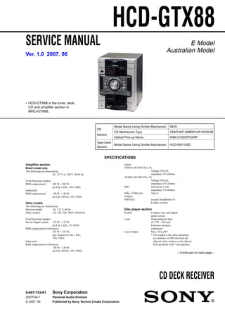
  • 1. 1 Ver. 1.0 2007. 06 Model Name Using Similar Mechanism NEW CD CD Mechanism Type CDM74KF-K6BD91UR-WOD//M Section Optical Pick-up Name KSM-213DCP/C2NP Tape Deck Model Name Using Similar Machanism HCD-GN1100D Section SERVICE MANUAL E Model Australian Model HCD-GTX88 Amplifier section Brazil model only The following are measured at AC 127 V or 220 V, 50/60 Hz Front/Surround speaker RMS output power: 205 W + 205 W (at 8 Ω, 1 kHz, 10% THD) Subwoofer RMS output power: 130 W + 130 W (at 6 Ω, 100 Hz, 10% THD) Other models The following are measured at Mexican model: AC 127 V, 60 Hz Other models: AC 120, 220, 240 V, 50/60 Hz Front/Surround speaker Power Output (rated): 175 W + 175 W (at 8 Ω, 1 kHz, 1% THD) RMS output power (reference): 255 W + 255 W (per channel at 8 Ω, 1 kHz, 10% THD) Subwoofer RMS output power (reference): 130 W + 130 W (at 6 Ω, 100 Hz, 10% THD) SPECIFICATIONS Inputs VIDEO (AUDIO IN) L/R: Voltage 250 mV, impedance 47 kilohms AUDIO (AUDIO IN) L/R: Voltage 450 mV, impedance 47 kilohms MIC: Sensitivity 1 mV, impedance 10 kilohms (USB) port: Type A Outputs PHONES: accepts headphones of 8 ohms or more Disc player section System Compact disc and digital audio system Laser Semiconductor laser (λ=770 – 810 nm) Emission duration: continuous Laser Output Max. 44.6 µW* * This output is the value measured at a distance of 200 mm from the objective lens surface on the Optical Pick-up Block with 7 mm aperture. Sony Corporation Personal Audio Division Published by Sony Techno Create Corporation 9-887-753-01 2007F04-1 © 2007. 06 – Continued on next page – CD DECK RECEIVER • HCD-GTX88 is the tuner, deck, CD and amplifier section in MHC-GTX88.
  • 2. 2 HCD-GTX88 SAFETY-RELATED COMPONENT WARNING!! COMPONENTS IDENTIFIED BY MARK 0 OR DOTTED LINE WITH MARK 0 ON THE SCHEMATIC DIAGRAMS AND IN THE PARTS LIST ARE CRITICAL TO SAFE OPERATION. REPLACE THESE COMPONENTS WITH SONY PARTS WHOSE PART NUMBERS APPEAR AS SHOWN IN THIS MANUAL OR IN SUPPLEMENTS PUBLISHED BY SONY. Frequency response 20 Hz – 20 kHz Wave length 770 – 810 nm Signal-to-noise ratio More than 90 dB Dynamic range More than 88 dB Tape deck section Recording system 4-track 2-channel stereo Frequency response 50 – 13,000 Hz (±3 dB), using Sony TYPE I tape Tuner section FM stereo, FM/AM superheterodyne tuner FM tuner section Tuning range Brazil model: 87.5 – 108.0 MHz (100 kHz step) Other models: 87.5 – 108.0 MHz (50 kHz step) Antenna FM lead antenna Antenna terminals 75 ohm unbalanced Intermediate frequency 10.7 MHz AM tuner section Tuning range Latin American and Oceanian models: 530 – 1,710 kHz (with the interval set at 10 kHz) 531 – 1,710 kHz (with the interval set at 9 kHz) Other models: 531 – 1,602 kHz (with the interval set at 9 kHz) 530 – 1,610 kHz (with the interval set at 10 kHz) Antenna AM loop antenna Antenna terminals External antenna terminal Intermediate frequency 450 kHz USB section Supported bit rate MP3 (MPEG 1 Audio Layer 3): 32 – 320 kbps, VBR Sampling frequencies MP3 (MPEG 1 Audio Layer 3): 32/44.1/48 kHz Transfer speed Full-Speed Supported USB device Mass Storage Class Maximum current 500 mA General Power requirements Mexican model: 127 V AC, 60 Hz Brazil model: 127 V or 220 V AC, 50/60 Hz, Adjustable with voltage selector Oceanian model: 230 – 240 V AC, 50/60 Hz Argentina model: 220 V AC, 50/60 Hz Other models: 120 V, 220 V or 230 – 240 V AC, 50/60 Hz, adjustable with voltage selector Power consumption 430 W Dimensions (w/h/d) (Approx.) 281 × 361 × 417 mm Mass (Approx.) 14.2 kg Design and specifications are subject to change without notice.
  • 3. 3 CAUTION Use of controls or adjustments or performance of procedures other than those specified herein may result in hazardous radiation exposure. HCD-GTX88 NOTES ON HANDLING THE OPTICAL PICK-UP BLOCK OR BASE UNIT The laser diode in the optical pick-up block may suffer electrostatic breakdown because of the potential difference generated by the charged electrostatic load, etc. on clothing and the human body. During repair, pay attention to electrostatic break-down and also use the procedure in the printed matter which is included in the repair parts. The flexible board is easily damaged and should be handled with care. Notes on Chip Component Replacement • Never reuse a disconnected chip component. • Notice that the minus side of a tantalum capacitor may be damaged by heat. Flexible Circuit Board Repairing • Keep the temperature of soldering iron around 270°C during repairing. • Do not touch the soldering iron on the same conductor of the circuit board (within 3 times). • Be careful not to apply force on the conductor when soldering or unsoldering. UNLEADED SOLDER Boards requiring use of unleaded solder are printed with the lead free mark (LF) indicating the solder contains no lead. (Caution: Some printed circuit boards may not come printed with the lead free mark due to their particular size) : LEAD FREE MARK Unleaded solder has the following characteristics. • Unleaded solder melts at a temperature about 40 °C higher than ordinary solder. Ordinary soldering irons can be used but the iron tip has to be applied to the solder joint for a slightly longer time. Soldering irons using a temperature regulator should be set to about 350 °C. Caution: The printed pattern (copper foil) may peel away if the heated tip is applied for too long, so be careful! • Strong viscosity Unleaded solder is more viscou-s (sticky, less prone to flow) than ordinary solder so use caution not to let solder bridges occur such as on IC pins, etc. • Usable with ordinary solder It is best to use only unleaded solder but unleaded solder may also be added to ordinary solder. This appliance is claassified as a CLASS 1 LASER product. This label is located on the rear exterior. NOTES ON LASER DIODE EMISSION CHECK The laser beam on this model is concentrated so as to be focused on the disc reflective surface by the objective lens in the optical pick- up block. Therefore, when checking the laser diode emission, observe from more than 30 cm away from the objective lens. Laser component in this product is capable of emitting radiation exceeding the limit for Class 1.
  • 4. 4 HCD-GTX88 MODEL IDENTIFICATION – MODEL NUMBER LABEL – MODEL PARTS No. GTX88: E2 3-113-126-0s GTX88: E51 3-198-009-0s GTX88: AUS 3-197-997-0s GTX88: AR 3-198-001-0s • Abbreviation E2 : 120V AC area in E model E51 : Chilean and Peruvian model AR : Argentina model AUS : Australian model PART No.
  • 5. 5 TABLE OF CONTENTS HCD-GTX88 1. GENERAL Guide to parts and controls ...................................................... 6 2. DISASSEMBLY 2-1. Case (Top) ......................................................................... 13 2-2. Loading Panel.................................................................... 13 2-3. Tuner Pack ......................................................................... 14 2-4. CD Block Section.............................................................. 14 2-5. Front Panel Section ........................................................... 15 2-6. Tape Mechanism Deck, Mic Board, USB Connector Board ....................................................... 15 2-7. Panel Board, Function Board, Jog Board .......................... 16 2-8. CD-SW Board ................................................................... 16 2-9. Cover (CDM) .................................................................... 17 2-10. Back Panel Section ............................................................ 17 2-11. Power Board Section ......................................................... 18 2-12. Main Board ....................................................................... 18 2-13. Subwoofer Board, Power Board........................................ 19 2-14. Power Transformer (T1200) .............................................. 19 2-15. BD91 Board ...................................................................... 20 2-16. Driver Board, SW Board, USB Board .............................. 20 2-17. Optical Pick-up ................................................................. 21 2-18. Sensor Board ..................................................................... 21 2-19. Motor (TB) Board ............................................................. 22 2-20. Motor (LD) Board ............................................................. 22 3. TEST MODE ..................................................................... 23 4. MECHANICAL ADJUSTMENTS ............................... 27 5. ELECTRICAL ADJUSTMENTS................................. 28 6. DIAGRAMS 6-1. Block Diagram — RF/Servo Section — ........................... 31 6-2. Block Diagram — Tape/Tuner Section — ........................ 32 6-3. Block Diagram — Main Section — .................................. 33 6-4. Block Diagram — USB Section — .................................. 34 6-5. Block Diagram — AMP/Subwoofer Section — ............... 35 6-6. Block Diagram — Display/Power Section — .................. 36 6-7. Circuit Boards Location .................................................... 37 6-8. Printed Wiring Board — BD91 Section — ....................... 40 6-9. Schematic Diagram — BD91 Section —.......................... 41 6-10. Printed Wiring Boards — Driver Section —..................... 42 6-11. Schematic Diagram — Driver Section — ......................... 43 6-12. Schematic Diagram — Main Section (1/4) — .................. 44 6-13. Schematic Diagram — Main Section (2/4) — .................. 45 6-14. Schematic Diagram — Main Section (3/4) — .................. 46 6-15. Schematic Diagram — Main Section (4/4) — .................. 47 6-16. Printed Wiring Board — Main Section — ........................ 48 6-17. Printed Wiring Board — USB Connector Section — ....... 49 6-18. Schematic Diagram — USB Connector Section — .......... 49 6-19. Printed Wiring Board — USB Section —......................... 50 6-20. Schematic Diagram — USB Section — ........................... 51 6-21. Printed Wiring Board — Effector Section — ................... 52 6-22. Schematic Diagram — Effector Section — ...................... 53 6-23. Printed Wiring Board — Panel Section —........................ 54 6-24. Schematic Diagram — Panel Section — .......................... 55 6-25. Printed Wiring Boards — Function Section —................. 56 6-26. Schematic Diagram — Function Section — ..................... 57 6-27. Printed Wiring Board — Power Amp Section — ............. 58 6-28. Schematic Diagram — Power Amp Section — ................ 59 6-29. Printed Wiring Board — Subwoofer Section — ............... 60 6-30. Schematic Diagram — Subwoofer Section —.................. 61 6-31. Printed Wiring Boards — Trans Section — ...................... 62 6-32. Schematic Diagram — Trans Section — .......................... 63 7. EXPLODED VIEWS 7-1. Main Section ..................................................................... 78 7-2. Front Panel Section (1)...................................................... 79 7-3. Front Panel Section (2)...................................................... 80 7-4. Front Panel Section (3)...................................................... 81 7-5. Chassis Section ................................................................. 82 7-6. CD Mechanism Section (1) ............................................... 83 7-7. CD Mechanism Section (2) ............................................... 84 8. ELECTRICAL PARTS LIST ........................................ 85
  • 6. 6 HCD-GTX88 SECTION 1 GENERAL This section is extracted from instruction manual. 6GB Guide to parts and controls This manual mainly explains operations using the buttons on the unit, but the same operations can also be performed using the buttons on the remote having the same or similar names. Unit – Front view – Top view qdqfqgqh 1 2 3 4 5 6 qj qk ql w; wa ws wd wf 7 8 9 q; qa qs wkwj wgwh
  • 7. 7 HCD-GTX88 7GB Guidetopartsandcontrols 1 FLANGER (pages 35, 43, 48) DELAY (pages 35, 43, 48) CHORUS (pages 36, 43, 48) SOUND FLASH (page 35) Press to create a party atmosphere. B Display (pages 9, 38, 39, 48) C SURROUND SPEAKER MODE (MHC-GTX88 only) (page 34) Press to select the sound system. SURROUND (MHC-GTX77/MHC-GTX66 only) (page 34) Press to select the surround effect. D Disc tray (pages 9, 17, 44, 48) E AMP MENU (page 38) Press to change the spectrum analyser display or to adjust the brightness of the display. F RETURN (pages 17, 25) Press to return to the parent folder. G NX (play/pause) (pages 17, 22, 24, 30, 44) Press to start or pause playback. x (stop) (pages 17, 23, 25, 28, 29, 30, 32, 44) Press to stop playback or recording. ./> (go forward/go backward) (pages 17, 20, 23, 25, 27, 31, 48) Press to select a track. TUNING +/– (pages 28, 29) Press to tune in a radio station. +/– (pages 17, 20, 23, 25, 27, 31) Press to select a folder. m/M (rewind/fast forward) (page 30) Press to fast forward or rewind. H CD- SYNC/REC 1 (page 22) Press to record from a disc onto the connected optional USB device (Digital music player or USB storage media). CD-TAPE SYNC (page 31) TAPE REC PAUSE/START (page 31) Press to record onto a tape. I PUSH OPEN/CLOSE Z (Deck B) (page 30) Press to insert or eject a tape. Deck B (pages 30, 31, 37, 48) J ENTER (pages 23, 29, 33, 48) Press to enter the selection. K ERASE (page 23) Press to erase MP3 audio tracks or folders on the connected optional USB device (Digital music player or USB storage media). L MASTER VOLUME (pages 17, 24, 39, 43) Turn to adjust the volume. M MIC (jack) (pages 36, 43, 52) Connect an optional microphone. MIC LEVEL (pages 32, 36, 43) Turn to adjust the microphone volume. USB Continued l
  • 8. 8 HCD-GTX88 8GB N REC/ERASE (indicator) (pages 23, 25) Lights up when recording from a disc onto the connected optional USB device (Digital music player or USB storage media). Lights up when erasing MP3 audio tracks from the connected optional USB device (Digital music player or USB storage media). O (USB) port (pages 22, 23, 24, 41, 52) Connect an optional USB device (Digital music player or USB storage media). P PHONES (jack) (pages 43, 52) Connect the headphones. Q Power illuminator (pages 35, 39) R PRESET EQ (page 33) Press to select a preset sound effect. S Z PUSH OPEN/CLOSE (Deck A) (page 30) Press to insert or eject a tape. Deck A (pages 30, 48) T Function buttons: CD (pages 14, 17, 22, 29, 31, 38) TUNER/BAND (pages 29, 38) TAPE A/B (pages 30, 38) AUDIO (pages 38, 41) VIDEO (pages 38, 41) (pages 23, 24, 26, 38) Press to select a function. U "/1 (on/standby) (pages 13, 14, 29, 43, 48) Press to turn the system on or off. V GROOVE (page 33) Press to reinforce the bass. W IR Receptor (page 43) X EQ BAND/MEMORY (page 33) Press to select a frequency band when adjusting the graphic equalizer. Y DISPLAY (pages 38, 39, 40) Press to change the information in the display. Z OPERATION DIAL (pages 17, 25, 33, 35, 38) Turn to select a track or folder. Turn to select a setting. wj ILLUMINATION (page 39) Press to change the power illuminator pattern. wk DISC SKIP/EX-CHANGE (pages 14, 17, 18, 20) Press to skip a disc. Press to exchange other discs during playback. Z OPEN/CLOSE (pages 14, 17, 44) Press to load or eject a disc. DISC 1 ~ 3 (pages 18, 20) Press to select a disc. Press to switch to CD function from other function. USB
  • 9. 9 HCD-GTX88 9GB Guidetopartsandcontrols – Display A Lights up when the USB function is selected (page 24). B “MP3” lights up when an MP3 audio track is recognized. “CD” lights up when a disc is recognized. C Indicates the type of MP3 audio track information that displayed (page 39). “ ” lights up when a track name is displayed. “ ” lights up when an artist name is displayed. “ ” lights up when a folder name is displayed. D Indicates the tuner band (page 28). E Lights up when the MP3 audio track contains ID3 tag information. F Displays the current status and information (page 39). G Indicators for the TUNER function (page 28). H Lights up when the Play Timer or Recording Timer is set (page 37). I Lights up when the Sleep Timer is activated (page 37). J Lights up during recording (pages 22, 31). K Indicators for the TAPE function (page 30). “ ” and “ ” lights up when the system is turned on. “ ” lights up when there is a tape in the deck. L Lights up when an optional USB device (Digital music player or USB storage media) is recognized (page 22). M Indicates the selected play mode (pages 19, 26). N Indicators for the disc tray (page 17). “ ” lights up when the disc is selected. “ ” lights up when there is a disc on the disc tray. “1”, “2” and “3” light up when the system is turned on. O Indicates the activated sound effect (pages 33, 35). Note “LINK”, “MATRIX SUR 1” and “MATRIX SUR 2” light up for MHC-GTX88 only. FM AM ID3 AUTO PRESET ST MONO MHz kHz TUNED REC PLAY SLEEP CD USB MP3 BOOSTER SUR FLANGER CHORUS DELAY MATRIX SUR 12 LINK Z GROOVE SHUF TAPE USB USB MEMORY PGM ALL 1 DISCS REP 1 SYNC A B1 2 3 qa q;qs 432 5 6 7 81 9qdqfqg MP3 REC A B Continued l
  • 10. 10 HCD-GTX88 10GB Subwoofer A (SS-WG88A) 1 SUBWOOFER ON/OFF (page 13) Press to turn the subwoofer on or off. 2 SUBWOOFER LEVEL (page 13) Turn to adjust the subwoofer level. Remote 1 "/1 (on/standby) (pages 13, 16, 43) Press to turn the system on or off. B CLOCK/TIMER SELECT (page 38) CLOCK/TIMER SET (pages 16, 37) Press to set the clock and the timers. C REPEAT/FM MODE (pages 21, 27, 29, 47) Press to change the Repeat Play setting. Press to select the FM monaural or stereo reception. D USB (page 24) Press to select the USB function. CD (page 17) Press to select the CD function. TUNER/BAND (page 28) Press to select the TUNER function. Press to select FM or AM band. FUNCTION (pages 30, 41) Press to select a function. 2 1 q; qa qs qd 3 4 5 2 6 7 9 8 qf 1qg
  • 11. 11 HCD-GTX88 11GB Guidetopartsandcontrols E ./> (go forward/go backward) (pages 17, 20, 23, 25, 27, 31, 37, 48) Press to select a track. +/– (tuning) (pages 28, 29) Press to tune in a radio station. m/M (rewind/fast forward) (pages 17, 25, 30) Press to find a point in a track. (play) (pages 17, 24, 30, 44) X (pause) (pages 17, 30) x (stop) (pages 17, 25, 28, 30, 32) Press to start, pause or stop playback. F ENTER (pages 16, 23, 28, 33, 37) Press to enter the selection. G DISC SKIP (pages 18, 20) Press to skip a disc. H +/– (pages 17, 20, 23, 25, 27, 31) Press to select a folder. I VOLUME +/–* (pages 17, 24, 39, 43) Press to adjust the volume. * The VOLUME + button has a tactile dot. Use the tactile dot as a reference when operating the system. J EQ (page 33) Press to select a preset sound effect. K CLEAR (pages 21, 27) Press to delete a pre-programmed track. L PLAY MODE/TUNING MODE (pages 19, 26, 28, 29, 44) Press to select the play mode of CD or USB function. Press to select the tuning mode. qd TUNER MEMORY (page 28) Press to preset a radio station. qf DISPLAY (pages 38, 39, 40) Press to change the information on the display. qg SLEEP (page 37) Press to activate the Sleep Timer.
  • 12. 12 HCD-GTX88 SECTION 2 DISASSEMBLY Note : Disassemble the unit in the order as shown below. 2-19. MOTOR (TB) BOARD (Page 22) 2-20. MOTOR (LD) BOARD (Page 22) 2-1. CASE (TOP) (Page 13) 2-2. LOADING PANEL (Page 13) SET 2-3. TUNER PACK (Page 14) 2-16. DRIVER BOARD, SW BOARD, USB BOARD (Page 20) 2-15. BD91 BOARD (Page 20) 2-17. OPTICAL PICK-UP (Page 21) 2-4. CD BLOCK SECTION (Page 14) 2-10. BACK PANEL SECTION (Page 17) 2-5. FRONT PANEL SECTION (Page 15) 2-18. SENSOR BOARD (Page 21) 2-9. COVER (CDM) (Page 17) 2-11. POWER BOARD SECTION (Page 18) 2-13. SUBWOOFER BOARD, POWER BOARD (Page 19) 2-14. POWER TRANSFORMER (T1200) (Page 19) 2-12. MAIN BOARD (Page 18) 2-6. TAPE MECHANISM DECK, MIC BOARD, USB CONNECTOR BOARD (Page 15) 2-8. CD-SW BOARD (Page 16) 2-7. PANEL BOARD, FUNCTION BOARD, JOG BOARD (Page 16)
  • 13. 13 HCD-GTX88 2-2. LOADING PANEL Note : Follow the disassembly procedure in the numerical order given. 2-1. CASE (TOP) 1 screw (case 3 TP2) 6 screw (case 3 TP2) 2 two screws (case 3 TP2) 7 two screws (case 3 TP2) 4 9 qs 3 two screws (+BVTP 3 × 10) 8 two screws (+BVTP 3 × 10) qa two screws (+BVTP 3 × 10) qd case (top) 5 panel (side-R) 0 panel (side-L) 3 loading panel 2 Pull-out the disc tray. 1 Turn the pulley to the direction of the arrow. pulley Front panel side CD mechanism deck (CDM74KF)
  • 14. 14 HCD-GTX88 2-3. TUNER PACK 2-4. CD BLOCK SECTION 3 tuner pack 2 wire (flat type) (9 core) (CN1) 1 two screws (+BVTP 3 × 8) 1 screw (+BVTP 3 × 8) 5 three screws (+BVTP 3 × 12) 2 lug 3 tapping screw 4 tapping screw 6 wire (flat type) (13 core) (CN701) qs CD block section 7 9 wire (flat type) (21 core) (CN5053) 0 CN903 (5P) qa CN901 (2P) 8 wire (flat type) (27 core) (CN5051)
  • 15. 15 HCD-GTX88 2-6. TAPE MECHANISM DECK, MIC BOARD, USB CONNECTOR BOARD 2-5. FRONT PANEL SECTION 0 front panel section 3 2 three screws (+BVTP 3 × 8)1 three screws (+BVTP 3 × 8) 4 wire (flat type) (17 core) (CN508) 5 wire (flat type) (11 core) (CN509) 7 CN503 (3P) 8 CN507 (8P) 9 CN903 (3P) 6 CN100 (4P) 1 three screws (+BVTP 2.6 (3CR)) 2 three screws (+BVTP 2.6 (3CR)) 5 two screws (+BVTP 2.6 (3CR)) 7 two screws (+BVTP 2.6 (3CR)) 9 two screws (+BVTP 2.6 (3CR)) 0 USB CONNECTOR board bracket (MIC shield) 8 MIC board 6 3 tape mechanism deck 4 knob (MIC)
  • 16. 16 HCD-GTX88 2-7. PANEL BOARD, FUNCTION BOARD, JOG BOARD 2-8. CD-SW BOARD 2 two screws (+BVTP 2.6 (3CR)) 3 two screws (+BVTP 2.6 (3CR)) 8 five screws (+BVTP 2.6 (3CR)) 9 four screws (+BVTP 2.6 (3CR)) 0 six screws (+BVTP 2.6 (3CR)) qj three screws (+BVTP 2.6 (3CR)) 4 PANEL board qa PANEL board qs knob (volume) qd nut qf holder (jog) qg knob jog assy qh gear (encoder) qk JOG board 1 CN956 (2P) 6 CN905 (2P) 7 CN904 (3P) 5 wire (flat type) (25 core) (CN900) 2 1 two screws (+BVTP 2.6 (3CR)) 3 two screws (+BTTP (M2.6)) 4 three screws (+BTTP (M2.6)) 5 CD-SW board 6 escucheon (CD)
  • 17. 17 HCD-GTX88 2-10. BACK PANEL SECTION 2-9. COVER (CDM) 1 two screws (+BVTP 3 × 10) 3 cover (CDM) CD mechanism deck 2 screw (+BVTP 3 × 10) 5 four screws (+BVTP 3 × 10) 7 two screws (+BVTP 3 × 10) 8 three screws (+BVTP 3 × 10) 6 two screws (+BVTP 3 × 10) 4 wire (flat type) (17 core) (CN1502) 1 CN1200 (3P) 2 CN1204 (4P) 3 CN1202 (2P) 9 CN580 (3P) 0 back panel section
  • 18. 18 HCD-GTX88 2-11. POWER BOARD SECTION 2-12. MAIN BOARD 2 two screws (+BV3 (3-CR)) 7 two screws (+BV3 (3-CR)) 8 screw (+BV3 (3-CR)) 9 screw (+BV3 (3-CR)) 3 DC fan(M892) 6 three screws (+BVTP 3 × 10) 0 two screws (+BVTP 3 × 10) qa POWER board section 1 CN581 (3P) 4 CN1214 (6P) 5 CN1212 (7P) 1 screw (+BVTP 3 × 10) 2 MAIN board POWER board assy CN600 CN601 CN700
  • 19. 19 HCD-GTX88 2-14. POWER TRANSFORMER (T1200) 2-13. SUBWOOFER BOARD, POWER BOARD 1 two screws (transistor) 9 two screws (transistor) qd screw (+BVTP 3 × 10) qf bracket qg POWER board qs heat sink assy 6 two screws (+BVTP 3 × 8) 7 holder 2 two screws (+BVTP 3 × 10) 8 two screws (+BVTP 3 × 10)0 two screws (+BVTP 3 × 10) qa 5 CN607 (5P) 4 SUBWOOFER board 3 screw (+BV3 (3-CR)) 2 two screws (+BV3 (3-CR)) 7 three screws 8 power transfomer (T1200) TRANS board 6 three screws 3 DC fan(M892) 4 CN1214 (6P) 5 CN1212 (7P) 1 CN581 (3P)
  • 20. 20 HCD-GTX88 2-15. BD91 BOARD 2-16. DRIVER BOARD, SW BOARD, USB BOARD 3 BD91 board 2 Remove the four solders. 1 wire (flat type) (16 core) (CN301) 2 CN703 (4P) 3 CN704 (2P) 5 DRIVER board 7 SW board 1 two screws (+BVTT (M2.6)) 6 screw (+BVTT (M2.6)) 8 two screws (+BVTP2.6 (3CR)) 9 USB board 4 wire (flat type) (5 core) (CN702)
  • 21. 21 HCD-GTX88 2-17. OPTICAL PICK-UP 2-18. SENSOR BOARD 3 two coil springs (insulator)5 two coil springs (insulator) 4 two insulators 6 two insulators 7 optical pick-up (BU-K6BD91UR) 1 two floating screws (+PTPWH M2.6) 2 two floating screws (+PTPWH M2.6) 2 tray 3 belt (table) 5 pulley (table) 8 screw (+BTTP (M2.6)) 0 SENSOR board 7 gear (geneva) 9 CN731 (3P) 1 floating screw (+PTPWH M2.6) 6 floating screw (+PTPWH M2.6) 4 floating screw (+PTPWH M2.6)
  • 22. 22 HCD-GTX88 2-19. MOTOR (TB) BOARD 2-20. MOTOR (LD) BOARD 6 Remove the two solderings of motor. 8 MOTOR (TB) board 7 table motor assy (M741) 5 two screws (+BTTP (M2.6)) 4 1 stopper 2 stopper table 3 wire (flat type) (5 core) (CN742) 2 Remove the two solderings of motor. 4 MOTOR (LD) board 1 belt (loading) 5 loading motor assy (M751) 3 two screws (+BTTP (M2.6))
  • 23. 23 HCD-GTX88 SECTION 3 TEST MODE 4. When the [MASTER VOLUME] knob is turned clockwise even slightly, the sound volume increases to its maximum and a message “VOLUME MAX” appears on the fluorescent indicator tube. 5. When the [MASTER VOLUME] knob is turned counter-clockwise even slightly, the sound volume decreases to its minimum and a message “VOLUME MIN” appears on the fluorescent indicator tube. * Tape function 1. Insert a tape in dack B. The function is changed to VIDEO automatically when the recording is started by pressing [CD- TAPE SYNC] then press [TAPE REC PAUSE/START] button. During recording theALC (Automatic Logic Control) is turned on. 2. During recording, press m button will stop the recording and the function is changed to TAPE B and rewind the tape in Deck B until the recording start position and playback of the tape in Deck B is started. If the [TAPE REC PAUSE/ START] button is pressed for a pause and pressed again to resume recording during recording time, when the tape is rewind, the tape will be rewind until the position where the pause is applied. * To release from MC Test mode 1. To release from this mode, press ?/1 button. 2. The cold reset is enforced at the same time. [COLD RESET] • The cold reset clears all data including preset data stored in the RAM to initial conditions. Execute this mode when returning the set to the customer. Procedure: 1. Press ?/1 button to turn on the system. 2. Press x button, [ENTER] button and ?/1 button simultaneously. 3. The message “COLD RESET” appears on the fluorescent indicator tube. Then, the fluorescent indicator tube becomes blank for while, and the set is reset. [VACS ON/OFF] • This mode is used to switch ON and OFF the VACS (Variable Attenuation Control System). Procedure: 1. Press ?/1 button to turn on the system. 2. Press x button and [ILLUMINATION] button simultaneously. The message “VACS OFF” or “VACS ON” appears on the fluorescent indicator tube. [TUNER STEP CHANGE] • The step interval of AM channels can be toggled between 9 kHz and 10 kHz. This mode is not available for Saudi Arabia model. Procedure: 1. Press ?/1 button to turn on the system. 2. Press [TUNER/BAND] button repeatedly to select the “AM”. 3. Press ?/1 button to turn off the system. 4. Press [ENTER] button and ?/1 button simultaneously. The system will turn on automatically. The message “AM 9K STEP” or “AM 10K STEP” appears on the fluorescent indicator tube and thus the channel step is changed. [GC TEST MODE] • This mode is used to check the fluorescent indicator tube, LEDs, buttons, MASTER VOLUME knob, OPERATION DIAL knob, model, destination, software version. Procedure: 1. Press x button, [ENTER] button and [DISC 2] button simultaneously. 2. All LEDs and segments in fluorescent indicator tube are lighted up. All LEDs are lighted up in red color except for NX LED where the LED is lighted up in green color. 3. When you want to enter to the model version and destination display mode, press [DISC 1] button. The model information appears on the fluorescent indicator tube. 4. Each time [DISC 1] button is pressed, the display changes to display software version and date of the software creation. The sequence is MC version, GC version, SYS version, CD version, CDDM version, CDMA version, CDMB version, BDA version, BDB version, ST version, TC version, TA version, TM version, MM1 version and MM2 version in this order, and returns to the model version display. 5. Press [DISC 2] button, the key check mode is activated. 6. In the key check mode, the fluorescent indicator tube displays “K 0 J0 V0”. Turn the [OPERATIONAL DIAL] clockwise; “J” value increases by one. Turn the [OPERATIONAL DIAL] counterclockwise; “J” value decreases by one. Each time a button is pressed, “K” value increases. Press other keys on main unit to check whether the key is detected. However, once a button has been pressed, it is no longer taken into account. “V” value increases in the manner of 0, 1, 2, 3 ... if [MASTER VOLUME] knob is turned clockwise, or it decreases in the manner of 0, 9, 8, 7 ... if [MASTER VOLUME] knob is turned counterclockwise. 7. When [DISC SKIP/EX-CHANGE] button is pressed after all LEDs and segments in fluorescent indicator tube light up, alternate segments in fluorescent indicator tube and LED would light up. If you press [DISC SKIP/EX-CHANGE] button again, another half of alternate segments in fluorescent indicator tube and LEDs would light up. Pressing [DISC SKIP/EX-CHANGE] button again would cause all LED and segments lights up. 8. To release from this mode, press three buttons in the same manner as step 1, or disconnect the power cord. [MC TEST MODE] • This mode is used to check operations of the respective sections of Amplifier, Tuner and Tape. Procedure: • To enter MC Test Mode 1. Press x button, [ENTER] button and [DISC 3] button simultaneously. 2. The CD ring indicators and TAPE A and B indicators flash on the fluorescent indicator tube. The function is changed to VIDEO. * Check of Amplifier 1. Press [EQ BAND/MEMORY] button repeatedly until a message “GEQ MAX” appears on the fluorescent indicator tube. GEQ increases to its maximum. 2. Press [EQ BAND/MEMORY] button repeatedly until a message “GEQ MIN” appears on the fluorescent indicator tube. GEQ decreases to its minimum. 3. Press [EQ BAND/MEMORY] button repeatedly until a message “GEQ FLAT” appears on the fluorescent indicator tube. GEQ is set to flat.
  • 24. 24 HCD-GTX88 [CD SERVICE MODE] • This mode let you move the CD sled motor freely. Use this mode when you want to clean the optical pick-up. Procedure: 1. Press ?/1 button to turn on the system. 2. Select CD function. 3. Press x button, [ENTER] button and [OPEN/CLOSE] button simultaneously. 4. The CD service mode is activated. The message “SERVICE MODE” appears on the fluorescent indicator tube. 5. With the CD in stop status, press M to move the optical pick-up to outside track, or turn m to move to inside track. The message “SLED OUT” or “SLED IN” appears on the fluorescent indicator tube. 6. To turn on or off the laser, press [FLANGER] button. The message “LD ON” or “LD OFF” appears on the fluorescent indicator tube. 7. To release from this mode, press ?/1 button to turn off the system. [CD AGING MODE] • This mode can be used for operation check of CD section. If an error occurs, the aging operation would stops and the status is displayed. If there were no error occurs, the aging operation would continue repeatedly. Procedure: 1. Press ?/1 button to turn on the system. 2. Select CD function. 3. Load three discs on disc tray. 4. Press [PLAY MODE/TUNING MODE] button on the remote control repeatedly to select the “ALL DISCS” mode, and press the [REPEAT/FM MODE] button on the remode control repeatedly to select repeat mode off. 5. Press x button, [ENTER] button and [DISC SKIP/EX-CHANGE] button simultaneously. 6. Aging operation is started. 7. To release from this mode, press ?/1 button or disconnect the power cord to turn the power OFF. • Aging mode sequence: DISC CHUCKING TOC READING PLAY FIRST TRACK FOR 2 SECONDS OPEN THE DISC TRAY DISC SKIP CLOSE THE DISC TRAY START PLAY LAST TRACK FOR 2 SECONDS EX-CHANGE OPEN/CLOSE CHANGE THE NEXT DISC
  • 25. 25 HCD-GTX88 [CD ERROR CODE MODE] • Display the CD error code when an error occurred. Procedure: 1. Press x button, [ENTER] button and [DISC 1] button simultaneously to enter the error code display mode. 2. The fluorescent indicator tube display the number of total error. 3. Each time m button and M button are turned, display change as below. %% : The process when trouble occurs 01 : Process ejecting DISC 02 : Process waiting for inserting DISC 03 : Process sending request to insert a disc to upper layer. 04 : Process sending request to eject a disc to upper layer. 05 : Process pulling a DISC in. 06 : Chucking process 07 : Re-chucking process 08 : Process cancelling chucking && : The operation when trouble occurs 00 : Waiting for operation. 10/11/12/13: During eject operation 20 : While pulling a disc in 30 : While cancelling chucking 40/41/42/43: During eject operation due to error. 0000 : Not used (Value is fixed to 0000). • Display of BD error. It is shown with “D” and 11 digits number. DISPLAY OF TOTAL ERROR DISPLAY OF MECHANICAL ERRORS BUTTONM m BUTTON DISPLAY OF NO DISC ERRORS BUTTONM m BUTTON M M M M 4. To clear the error record, operate the cold reset. (Refer to the “MC COLD RESET”.) 5. To release from this mode, press the ?/1 button or disconnect the power OFF. • Display of total error Em** : The number of times for CDM (mechanical) errors. Ed** : The number of times for BD error (after chucking the disc.). • Display of CDM (mechanical) error. It is show with “M” and 11 digit number. Em**Ed** M*$$%%&&0– 000 M* : The number of history error for mechanical. (“0” is latest one) (Turn > button to display next error.) $$ : Mechanical errors occur in the operation. FF : Mechanical error during normal operation. Other: Mechanical error during initializing operation. D*$$%%&&#– #00 D* : The number of error history (“0” is latest one) (Press > button to display next error.) $$ : The detail of trouble 01 : Can not focus 02 : GFS error 03 : Start-up time over 04 : Continuously out of focus 05 : Q code is not input for certain time 06 : Tracking on is impossible 07 : Blank disc %% : The process when trouble occurs 01 : While SHIP process is performed 02 : While POWER OFF is processed 03 : While INITIALIZE (POWER ON) is processed. 04 : While oscillation stops 05 : From stopping oscillation to start oscillation 06 : During stop 07 : During STOP operation 08 : While start-up is processed 09 : While TOC reading is processed 0a : During search operation 0b : During PLAY operation 0c : During pause operation 0d : During PLAY manual search operation 0e : During PAUSE manual search operation && : Processing operation when trouble occurs Show each STEP mentioned in %% digits. ## : Disc speed when trouble occurs. 01 : x1 speed 02 : x2 speed (for models which support x2 speed) 04 : x4 speed 00 : Not used (value is fixed to 00).
  • 26. 26 HCD-GTX88 [CD REPEAT 5 LIMIT OFF MODE] • The number of repeat for CD playback is 5 times when the re- peat mode is “REPEAT ALL”. This mode enables CD to repeat playback for limitless times. Procedure: 1. Press ?/1 button to turn on the system. 2. Select CD function. 3. Press x button, [CD] button and [DISC 1] button simultaneously to enter the CD repeat 5 limit off mode and the fluorescent indicator tube displays “LIMIT OFF”. • To release from this mode, operate the cold reset. (Refer to the “MC COLD RESET”.) [CD SHIP MODE (WITH MEMORY CLEAR)] • This mode moves the optical pick-up to the position durable to vibration and clears all data including preset data stored in the RAM to initial conditions. Use this mode when returning the set to the customer after repair. Procedure: 1. Press ?/1 button to turn on the system. 2. Select CD function. 3. Press x button, [SOUND FLASH] button and ?/1 button simultaneously. The system will turn off automatically. 4. After the “STANDBY” blinking display finishes, a message “MECHA LOCK” is displayed on the fluorescent indicator tube and the CD ship mode is set. 5. The Memory is clear after AC Power OFF. [CD SHIP MODE (WITHOUT MEMORY CLEAR)] • This mode moves the optical pick-up to the position durable to vibration. Use this mode when returning the set to the customer after repair. Procedure: 1. Press ?/1 button to turn on the system. 2. Select CD function. 3. Press [CD] button and ?/1 button button simultaneously. The system will turn off automatically. 4. After the “STANDBY” blinking display finishes, a message “MECHA LOCK” is displayed on the fluorescent indicator tube and the CD ship mode is set. [CD/USB POWER MANAGE] • This mode let you switch on or off power supply to the BU and USB Micom during TUNER function. • When CD and USB POWER is set to OFF, the power supply to the BU and USB Micom is cut off during TUNER function. It will increase the time taken to access CD and USB when function change from TUNER to CD or USB but it will improve tuner reception. • When CD and USB POWER is set to ON, the power supply to the BU and USB Micom is not cut off during TUNER function. It will reduce the time taken to access CD or USB when function change from TUNER to CD or USB but it will decrease tuner reception performance. Procedure: 1. Press ?/1 button to turn on the system. 2. Select CD section. 3. Press ?/1 button to turn off the system. 4. When demonstration appear, press x button and ?/1 button simultaneously. The set will power on automatically. 5. The message “CD/USB POWER ON” or “CD/USB POWER OFF” will be displayed on the fluorescent indicator tube. [CD TRAY LOCK MODE] • This mode let you lock the disc tray.When this mode is activated, the disc tray will not open when [OPEN/CLOSE] button or [DISC SKIP/EX-CHANGE] button is pressed. The message “LOCKED” will be displayed on the fluorescent indicator tube. Procedure: 1. Press ?/1 button to turn on the system. 2. Select CD function. 3. Press x button, [OPEN/CLOSE] button simultaneously and hold down until “LOCKED” or “UNLOCKED” displayed on the fluorescent indicator tube (around 5 seconds). [TCM OFFLINE MODE] • This mode is used to prevent the system from turning off auto- matically when TCM is not connected. Therefore, measurements can be done even when TCM is not connected during produc- tion. Procedure: 1. When the system is turned off, press [EQ BAND/MEMORY] button, [TAPE A/B] button and ?/1 button simultaneously. The system will turn on automatically. 2. The message “TCM OFFLINE” will be displayed on the fluorescent indicator tube. • To release from TCM Offline Mode, perform “COLD RESET” or turn off the power supply. [VACS DISPLAY] • This mode is used to check the VACS level. Procedure: 1. Press ?/1 button to turn on the system. 2. Press x button, [CHORUS] button and [DISC SKIP/EX- CHANGE] button simultaneously. 3. TheVACS Level Display, the fluorescent indicator tube displays “VATB F APC”. “V” represent VACS, A represent VACS level which is triggered by signal level, “T” represent ThermalVACS NEO, B representVACS level which is triggered by temperature, “F” represent FAN is triggered by software to turn in to high speed, “AP” represent APVACS (Abuse Protection VACS) and “C” represent APVACS level which is triggered.
  • 27. 27 HCD-GTX88 [ERROR MESSAGE] 1. GC error message • Display Display on fluorescent indicator tube, GC ERR01 When “GC ERR01” message appears, all LEDs lights up and set becomes hang. Set does not respond to any main unit keys or remote controller keys. • What to do 1. Please check the model resistor value and replace with correct parts. 2. Plug in the set. The error message shall not be appear. Precaution 1. Clean the following parts with a denatured alcohol-moistened swab: record/playback heads pinch rollers erase head rubber belts capstan idlers 2. Demagnetize the record/playback head with a head demagnetizer. 3. Do not use a magnetized screwdriver for the adjustments. 4. After the adjustments, apply suitable locking compound to the parts adjusted. 5. The adjustments should be performed with the rated power supply voltage unless otherwise noted. Torque Measurement 2.9m N • m to 6.9m N • m FWD CQ-102C 30 to 70 g • cm (0.42 – 0.97 oz • inch) FWD 0.15m N • m to 0.59m N • m back tension CQ-102C 2 to 6 g • cm (0.03 – 0.08 oz • inch) 2.9m N • m to 6.9m N • m REV CQ-102RC 30 to 70 g • cm (0.42 – 0.97 oz • inch) 0.15m N • m to 0.59m N • mREV CQ-102RC 2 to 6 g • cmback tension (0.03 – 0.08 oz • inch) 4.8m N • m to 16.7m N • m FF/REW CQ-201B 49 to 170 g • cm (0.68 – 2.36 oz • inch) Mode Torque meter Meter reading SECTION 4 MECHANICAL ADJUSTMENTS
  • 28. 28 HCD-GTX88 [FM Tune Level Check] Procedure: 1. Turn the power on. 2. Input the following signal from Signal Generator to FM antenna input directly. * Carrier Freq: A = 87.5 MHz, B = 98 MHz, C = 108 MHz Deviation : 75 kHz Modulation : 1 kHz ANT input : 35 dBu (EMF) Note: Please use 75 ohm “coaxial cable” to connect SG and the set. You cannot use video cable for checking. Please use SG whose output impedance is 75 ohm. 3. Set to FM tuner function and tune A, B and C signals. 4. Confirm “TUNED” is lit on the display forA, B and C signals. The mark of “TUNED” means “The selected station signal is received in good condition.” FM signal generator OUT (75 Ω) SET SECTION 5 ELECTRICAL ADJUSTMENTS 1. Demagnetize the record/playback head with a head demagnetizer. 2. Do not use a magnetized screwdriver for the adjustments. 3. After the adjustments, apply suitable locking compound to the parts adjust. 4. The adjustments should be performed with the rated power supply voltage unless otherwise noted. 5. The adjustments should be performed in the order given in this service manual. (As a general rule, playback circuit adjustment should be completed before performing recording circuit adjustment.) 6. The adjustments should be performed for both L-CH and R- CH. 7. Switches and controls should be set as follows unless otherwise specified. • Test Tape [RECORD/PLAYBACK HEAD AZIMUTH ADJUST-MENT] DECK A DECK B Note: Perform this adjustments for both decks Procedure: 1. Mode: Playback 2. Turn the adjustment screw and check output peaks. If the peaks do not match for L-CH and R-CH, turn the adjustment screw so that outputs match within 1dB of peak. Tape Signal Used for P-4-A100 10 kHz, –10 dB Azimuth Adjustment set MAIN board CN510 Pin 1 (L-CH) Pin 3 (R-CH) MAIN board CN510 Pin 2 (GND) + – level meter test tape P-4-A100 (10 kHz, –10 dB) screw position L-CH peak within 1dB output level L-CH peak R-CH peak within 1dB screw position R-CH peak TUNER SECTION 0 dB = 1 µV DECK SECTION 0 dB = 0.775 V
  • 29. 29 HCD-GTX88 CD SECTION [TEST DISC LIST] Use the following test disc on test mode. • CD: YEDS-18 (PART No. 3-702-101-01) or PATD-012 (PART No. 4-225-203-01) Note: 1. CD Block is basically designed to operate without adjustment. Therefore, check each item in order given. 2. Use YEDS-18 (3-702-101-01) unless otherwise indicated. 3. Use an oscilloscope with more than 10MW impedance. 4. Clean the object lens by an applicator with neutral detergent when the signal level is low than specified value with the following checks. [S-CURVE CHECK] Procedure : 1. Connect an oscilloscope to TP106 (FE) and TP124 (VC). 2. Turn the power on. 3. Load a disc (YEDS-18) and actuate the focus search. (In consequence of open and close the disc tray, actuate the focus search) 4. Confirm that the oscilloscope waveform (S-curve) is symmetrical between A and B. And confirm peak to peak level within 3 ± 0.5 Vp-p. Note: • Try to measure several times to make sure than the ratio of A : B or B : A is more than 10 : 7. • Take sweep time as long as possible and light up the brightness to obtain best waveform. 3. Mode: Playback 4. After the adjustments, apply suitable locking compound to the pats adjusted. Adjustment Location: Playback Head (Deck A). Record/Playback/Erase Head (Deck B). MAIN board CN510 test tape P-4-A100 (10 kHz, –10 dB) pin 3 oscilloscope L-CH R-CH V H waveform of oscilloscope in phase 45° 90° 135° 180° good wrong pin 2 pin 1 L R forward reverse + – TP106(FE) TP124(VC) oscilloscope BD91 board symmetry S-curve waveform within 3 ±0.5Vp-p A B
  • 30. 30 HCD-GTX88 [RF LEVEL CHECK] Procedure : 1. Connect an oscilloscope to TP123 (RFO) and TP124 (VC). 2. Turn the power on. 3. Load a disc (YEDS-18) and playback. 4. Confirm that oscilloscope waveform is clear and check if RF signal level is correct or not. Note: Clear RF signal waveform means that the shape “ ◊ ” can be clearly distinguished at the center of the waveform. Connecting Location: CD board + – TP123(RFO) TP124(VC) oscilloscope BD91 board VOLT/DIV: 200 mV TIME/DIV: 500 ns RF signal waveform level: 1.3 ± 0.3 Vp-p IC401 – BD91 Board (SIDE B) – TP124 (VC) TP123 (RFO) TP106 (FE) IC101 1 1 14 1528 25 26 50 5175 76 100
  • 31. 31 31 HCD-GTX88 HCD-GTX88 6-1. BLOCK DIAGRAM — RF/SERVO SECTION — (Page 34) SECTION 6 DIAGRAMS DETECTOR 97 95 94 96 98 100 FNI1 FPI1 FNI2 FPI2 TPI TNI LD0 MDI CD RF AMP, FOCUS/TRACKING ERROR AMP, DIGITAL SIGNAL PROCESSOR, DIGITAL SERVO PROCESSOR, DIGITAL FILTER,D/A CONVERTER IC101 OPTICAL PICK-UP BLOCK (KSM-213DCP) 2AXIS DEVICE FOCUS/ TRACKING COIL 91 92 26 27 24 AUTOMATIC POWER CONTROL Q301 LASER DIODE FOCUS COIL DRIVE 18 17 20 TRACKING COIL DRIVE 12 9 13 10 FOCUS/TRACKING COIL DRIVER, SPINDLE, SLED MOTOR DRIVER IC401 2 1 SPINDLE MOTOR DRIVEMM M401 (SPINDLE) MM M402 (SLED) FMO FOO DND TRO 23 XI 24 XO VREF FOO B C D F E LD PD FCS+ FCS– SL– SL+ SP+ SP– TRK+ TRK– VC VREF VREF11 PREF77 VRO84 SLED MOTOR DRIVE 23 7 XRST1 24 SBSY19 BIAS MUTE MMUTE2 4I/O11 TRO FMO FOO DMO TRO FMO DMO 30 27 CD+1.5V REG IC201 DVDD+3.3VCD+1.5V LO RO CD LCH CD RCH 47AOUT2(PO5) DATA 63BCK(PO8) CLK 51PIO3 GATE 49PIO1 ST REQ 65AIN(PI4) AIN 66BCKI(PI5) BCKIN 67LRCKI(PI6) SELECT112 1B3 1Y 4C 3C 2C 1C 4 2Y 7 1A2 2A5 2B6 3A11 6 5 13 4O/I 3I/O 3O/I 2I/O 2O/I 1I/O 1O/I 10 23 22 21 6 39 3 5 38BUS0 9 8 39BUS1 3 4 40BUS2 (SO) 1 2 11 10 9 8 3 4 1 2 41BUS3 (SI) 48PIO1 LRCKIN BUS3 BUS2 BUS1 BUS0 3Y 9 4Y 12 REQ CCE 3B10 4A14 4B13 BUCK VM+7V 20 IO0(/HSO) USB SECTIONB MAIN SECTIONA • Signal Path 11 12 9 3 93CCE BUS0 BUS1 BUS2 BUS3 SEL SW CDCLK CDCCE MP3IREQ 42BUCK 37RST 54SBSY 4I/O 124C 3C 2C 1C 6 5 13 4O/I 3I/O 3O/I 2I/O 2O/I 1I/O 1O/I 21 • 22 X102 16.934MHz S201 (LIMIT) DVDD+3.3V SYSTEM CONTROL IC401 (1/6) SELECT SWITCH IC567 SELECT SWITCH IC566 SELECT SWITCH IC568 SELECT SWITCH Q602 A : CD PLAY : DIGITAL : USB (Page 33)
  • 32. 3232 HCD-GTX88 HCD-GTX88 6-2. BLOCK DIAGRAM — TAPE/TUNER SECTION — (Page 33) (Page 33) (Page 33) ST-L E MAIN SECTION REC-OUT-L REC-OUT-L D MAIN SECTION TAPE MECHANISM BLOCK 32 A TRIGGER DRIVE Q340,343 R-CH TU901 FM/AM TUNER UNIT ANTENNA ST-L FM ANT AM ANT AM ANT ST-R ST-DIN/MC-DOUT ST-DOUT ST-CLK ST-CE FM 75 COAXIAL CAP M+ BTRGM+ ATRGM+ AHALF BHALF B SHUT A SHUT REC(FWD) CAPM-CONT B-TRIG A-TRIG TC-RELAY A-HALF B-HALF B-SHUT A-SHUT REC BIAS PB-A/B ALC REC-MUTE TC-MUTE AM EQ OUT1A B ST-DIN/MC-OUT SY-DOUT/MC-DIN ST-CLK ST-CE 34 28 27 26 2421 55 57 58 59 60 42 3 90 89 91 52 56 51 54 53 E-1 45 E-2 44 E-3 43 86 84 85 87 13 11 15 14 PB OUT1TAI1 REC IN1 AIN1 BIN1 A/B ALCON/OFF RECMUTEON/OFF MUTEON/OFF DECK A/B SELECT, PB/REC EQUALIZER AMP IC301 SYSTEM CONTROL (TAPE MECHANISM CONTROL) IC401 (2/6) REC-OUT1 EQ TC-PB-L TEST CONNECTOR CN510 R-CH R L C MAIN SECTION PB HEAD DECK-A DECK-B BIAS OSC Q370 BIAS TRAP MUTE CONTROL SWITCH Q377, 379 TC PB MUTE CONTROL SWITCH Q382.383 R-CH R-CH Q376 Q373,374 Q381 L – CH R – CH R-CH BIAS+9V REC/PB HEAD ERASE HEAD Q378,380 T301 L – CH R – CH • R-CH is omitted due to same as L-CH. A TRIGGER DRIVE Q342,345 CAPSTAN MOTOR DRIVE Q341,344 4 1 2 TABLE ADDRESS SENSOR IC731 LD MOTOR DRIVER IC701 TBL MOTOR DRIVER IC712 M+9V Q731 MOTOR DRIVE M751 (TABLE LOADING) M RE701 ROTARY ENCODER DISC TRAY ADDRESS DETECT S751 OPEN/CLOSE DETECT LM-F TBL SENS FIN RIN 48 OPENSW 41 LM-R 49 7 9 OUT2 OUT1 2 4 MOTOR DRIVE M741 (TABLE) M TM-F FIN RIN 46 TM-R 47 7 9 OUT2 OUT1 2 4 : TAPE PLAY (DECK B) : TAPE PLAY (DECK A) : TUNER : RECORD (DECK B) • Signal Path : AUDIO
  • 33. 33 33 HCD-GTX88 HCD-GTX88 6-3. BLOCK DIAGRAM — MAIN SECTION — (Page 31) (Page 35) (Page 32) (Page 35) (Page 32) (Page 36) (Page 32) (Page 35)J101 RCH L CD LCH CD RCH R AUDIO IN CD RCH 11 10 9 3 RCH MIXER IC1500 MULTIPLEXER IC1503 DIGITAL DELAY IC1501 SIGNAL SELECTER IC564 SURROUND VOLUME CONTROL IC201 INPUT SELECT SWITCH, GRAPHIC EQUALIZER CONTROL, ELECTRICAL VOLUME IC101 SIGNAL SELECTER IC563 MIC AMP IC1100 (1/2) MIC AMP IC1100 (2/2) RV1150 MIC LEVEL LPF1IN A B C COM CD A-MUTE SOURCE SEL 2 SOURCE SEL 1 CTRL 1 CTRL 3 DATA CLK Z GROOVE FREQ LINE MUTE EFFECTOR SYSTEM CONTROL IC401 (3/6) S0 S1 S2 SEL 9LPF2OUT 19SAOUT A+9V L+R SPEANA J1100 (2/2) 10LPF2IN 11OP2OUT 12OP2IN LPF1OUT CLOCK14 3 2 25 26 2771865 28 78 77 81 82 75 80 79 66 RCH L R VIDEO IN MIXER IC1505 BUFFER Q1513 MUTE Q250 CD MUTE Q540 DBFB SWITCH Q101SELECT SWITCH Q596 SELECT SWITCH Q597 BUFFER Q1509 EFFECTOR SELECT SWITCH Q598 XRF/SERVO SECTION A ST L TC PB L XTAPE/TUNER SECTION TAPE/TUNER SECTION E X DISPLAY/POWER SECTION G X AMP/SUBWOOFER SECTION I REC OUT L X TAPE/TUNER SECTION D X AMP/SUBWOOFER SECTION F X AMP/SUBWOOFER SECTION H XC 4 IMB1 DBFB F/B SWITCH Q608 SWITCH Q591 3 INA1 6 IND1 14 LFE VOL IN 2 MIC 8RECB1 F–L18OUT1 24SWOUT 16BB A1 17BB B1 11TCA1 21DATA 22CLOCK 12TCB1 SW OUT34FL OUT 17DATA 18CLOCK MUTE Q180 D+4V REG Q325 MUTE Q607 LINE MUTE Q544 1 5 3 10 Y0 Y1 Y A D101,102 J103 EXCEPT AUS MODEL D-LIGHT SYNC OUT 3 2 9 10 Y1 Y2 Y3 A B Y 5 4 J1100 (1/2) MIC Q1500 Q1508 Q1506 Q1502 RCH M61529 DATACLK M61530 7 13 5 3 : AUDIO : CD PLAY : TAPE PLAY (DECK A) : TAPE PLAY (DECK B) : MIC : TUNER • Signal Path • R-CH is omitted due to same as L-CH. • Abbreviation AUS : Australian model
  • 34. 3434 HCD-GTX88 HCD-GTX88 6-4. BLOCK DIAGRAM — USB SECTION — (Page 31) 77 78 3 45 VBUS+5V USB CONTROL IC901 VBUS POWER ON/OFF SWITCH IC915 SYSTEM CONTROL IC401 (4/6) S-RAM IC921 CN952 1 4 (USB) VBUS D– D+ GND OUT P75/USBOC P76/USBPON D– OE A0 I A2 A3 I A6 A7 I A10 A11 I A15 WE LB UB CE D+ IN FLG EN 1 80 79 PF1/RXDODATA 85 PF2/SCLK0/CTSO/CLK/TB0OUT0CLK 86 PN5/HSS1/SCL1GATE 94 PN4/HSS0/SDA1A IN 93 PN3/HSCLKBCK IN 92 P83/CS3/WAIT/TA5OUTLRCKIN 71 P64/A20 P63/A19 P62/A18 P61/A17 USBRST USB SERIAL TXDO USB SERIAL RXDO USB SERIAL RTSO USB SERIAL CTSO BUS3 58 BUS2 57 BUS1 56 BUS0 55 P66/A22CCE 60 P65/A21BUCK 59 PG3REQ 96 PG2ST REQ 97 P70/RD P71/SRWR 18 I 25 • 28 I 35 64 41 1765 P72/SRLLB P73/SRLUB 66 39 4067 P82/CS2 70 16 RESET PC0/INT0 1 31 382 PF0/TXD0 PF4/RXD1/SPDI 84 34 3588 PF3/TXD1/SPD0 87 X1 75 X2 73 36 P00/D0 I P07/D7 P10/D8 I P17/D15 37 I 43 • 46 I 54 44 I 42 • 27 I 24 • 21 I 18 • 5 I 1 I/O0 I I/O3 I/O4 I I/O7 I/O8 I I/O11 I/O12 I I/O15 7 I 10 • 13 I 16 • 29 I 32 • 35 I 38 P41/A1 I P47/A7 P50/A8 I P60/A16 RF/SERVO SECTION B X901 9kHz • Signal Path : USB : DIGITAL
  • 35. 35 35 HCD-GTX88 HCD-GTX88 6-5. BLOCK DIAGRAM — AMP/SUBWOOFER SECTION — (Page 33) (Page 33) (Page 36) (Page 36) (Page 33) MUTING Q604, 606, 610 F-R DBFB F/B F-L 67 STKMUTE 12 OVER LOAD DETECT Q668, 618 + + + MUTE Q640, 641 MUTE CONTROL Q634,682,684 71 LINKRELAY 88 FANHISPEED 97 SWVOLLED 100 HPDET 95 SWVOLIN RELAY DRIVE Q644, 647 +VL –VL IN1 ST BY +RE1 –RE1 +RE2 –RE2 +VCC –VCC SW OUT + - - + FRONT SPEAKER SUB WOOFER OUT L R PHONES J1101 RY646 RY862 + - - + L R FAN MOTOR DRIVE Q579, 585 DC FAN M891 M M FAN MOTOR DRIVE Q586–588 FAN CONTROL SWITCH Q584 FAN DETECT Q580–582 DC FAN M892 TH629 THERMAL DETECT Q628, 630 94 THERMALVACS TB001 TM600 D624 D550 18 11 10 9 14 8 • SIGNAL PATH POWER AMP IC601 69 PROTECTOR 70 FRONTRELAY 68 HPMUTE H MAIN SECTION FMAIN SECTION MAIN SECTION I DISPLAY /POWER SECTION K DISPLAY/ POWER SECTION J TH630 11 4 5 6 7 3 2 13 OCP CT OUT VL(AC) 1 VP2 4 3 STK MUTE Q812 SUBWOOFER POWER AMP IC800 SYSTEM CONTROL IC401 (5/6) OVER CURRENT PROTECTOR IC550 OVERLOAD DETECT Q850 AC OUT DETECT Q815 UNDER VOLTAGE DETECT SWITCH Q506 RELAY DRIVE Q814 OVERLOAD DETECT Q800 OVERLOAD DETECT SWITCH Q648 RY665 FAN CONTROL HI SPEED SWITCH Q581 SYSTEM CONTROL +9V CN102 + - - + SURROUND SPEAKER L R TM601 RELAY DRIVE Q666 72 SWSPKRELAY 61 UNDERVOLTAGEDET • R-CH is omitted due to same as L-CH. : AUDIO
  • 36. 3636 HCD-GTX88 HCD-GTX88 6-6. BLOCK DIAGRAM — DISPLAY/POWER SECTION — USB +5V ND900 VACUUM FLUORESCENT DISPLAY 9,10,12–22, 24–41,43–47 1–6,87-100 P1–36G2–21 64–66 7,8,86 BF4 1 SPECTRUM ANALYZER IC902 67 6816 2 15 69 71 48 80 ALL BAND BF3 BF1 IN2 IN1 VKK LED SELECTOR G1,22,23 G1,22,23 G2-21 13 17 73 VOLUMEMASTER VOLUME SPEANA P1 – 36 VF1 VF2 D900 –VG (–32V) FUN CONTROL X900 4MHz 83 XI 82 XO 52–59, 75,76,78,79 LED DRIVE Q906–911, 913–916 920,921 D906, 908, 910, 913, 917, 921, 929, 923, 925, 927 D905, 907, 909, 912, 914, 916, 922, 924, 926.955 LED+9V Q903 Q902 Q901 Q900 D904 (R) D930 (G) KEY2 | KEY0 S901 – 914, 916 –933 60I2C DATA 61I2C CLK 77RESET 30 IIC-DATA 29 IIC-CLK IIC-DATA IIC-CLK 37 GC-RESET 74 POWER-KEY 73 DISPLAY-KEY S934 S900 DISPLAY 33 STBY-LED/FAN CONTROL 4 SIRCS RESET X402 5MHz 15 X-IN 13 X-OUT X401 32.768kHz 10 XC-IN 11 XC-OUT SYSTEM CONTROL IC401 (6/6) 50STBY-RELAY 12RESET 20AC-CUT D671 D402 D501,504 POWER SWITCHING LED DRIVE Q904,905 RECT D658 RECT D656 +VL VL(AC) F1261 VL VL VH VH VP VF VF GNDF1271 F1241 F1251 R1292 –VL +VH –VH – 33V REGULATOR Q1264 POWER ON/OFF RELAY DRIVE Q1200 – VG (-32V) D1292 RECT VF1 VF2 ND900 VACUUM FRUORESCENT DISPLAY RY1200 AC IN T1200 POWER TRANSFORMER RESET SWITCH Q501 REMOTE CONTROL SIGNAL RECEIVER IC901 EVER +4V D+3.3V DISPLAY CONTROL, KEY CONTROL IC900 BUFFER Q917, 918, 919 70 BF214 72 OPERATION DIALROTARY ENCODER ROTARY ENCODER OPERATION DIAL NO402 (FOR CHECK) CN402 (3/3) (FOR CHECK) 40USB-POWER 63OVER VOLTAGE DET 32CD POWER USB POWER CONTROL SWITCH Q590,603 RECT D540 M +9V VM +7V LED +9V A +9V ST +9V OVER VOLTAGE DETECT SWITCH Q550 AC3 AC3F1281 AUDIO +9V BIAS +9V UNREG S1200 S1200 230 – 240V | 220V | 120V VOLTAGE SELECTOR AUS,AR MODEL E2,E51 MODEL S936 S935 XMAIN SECTION G XAMP/SUBWOOFER SECTION K XAMP/SUBWOOFER SECTION J LEVEL DETECT IC402 USB+5V REG IC565 +9V REG IC560 +9V REG IC561 DVDD+3.3V REG IC562 D592 D561, 562 D590,594 E2,E51 MODEL D593 DVSS +3.3V D +3.3V AVDD +3.3V DVDD +3.3V USB POWER CONTROL SWITCH Q604–606 CD POWER CONTROL SWITCH Q560,561 USB+9V REG IC570 D+4V REG IC569 • Abbreviation AR : Argentina model AUS : Australian model E2 : 120V AC area in E model E51 : Chilean and Peruvian model (Page 33) (Page 35) (Page 35)
  • 37. 37 HCD-GTX88 6-7. CIRCUIT BOARDS LOCATION MOTOR (LD) board SENSOR board SW board MOTOR (TB) board DRIVER board MAIN board MIC board JOG board FUNCTION board PANEL board BD91 board USB board USB CONNECTOR board POWER board TRANS board PRIMARY board CD-SW board TUNER PACK EFFECTOR board SWITCHING POWER SUBWOOFER board
  • 38. 38 HCD-GTX88 • Note For Printed Wiring Boards And Schematic Diagrams Note on Printed Wiring Board: • X : parts extracted from the component side. • Y : parts extracted from the conductor side. • : Pattern from the side which enables seeing. (The other layer’s patterns are not indicated.) Caution: Pattern face side: Parts on the pattern face side seen from (Conductor Side) the pattern face are indicated. Parts face side: Parts on the parts face side seen from (Component Side) the parts face are indicated. • Indication of transistor. • A : B+ Line. • B : B– Line. • Voltage and waveforms are dc with respect to ground under no-signal (detuned) conditions. • BD91 and Driver sections. no mark : CD PLAY • Except BD91 and Driver sections. no mark : FM ( ) : CD PLAY < > : TAPE PLAY [ ] : TAPE REC ∗ : Impossible to measure • Voltages are taken with a VOM (Input impedance 10 MΩ). Voltage variations may be noted due to normal produc- tion tolerances. • Waveforms are taken with a oscilloscope. Voltage variations may be noted due to normal produc- tion tolerances. • Circled numbers refer to waveforms. • Signal path. F : AUDIO f : TUNER E : TAPE PLAY (DECK A) d : TAPE PLAY (DECK B) G : TAPE REC (DECK B) N : MIC J : CD PLAY c : DIGITAL I : USB • Abbreviation AR : Argentina model AUS : Australian model E2 : 120V AC area in E model E51 : Chilean and Peruvian model Note: The components identified by mark 0 or dotted line with mark 0 are critical for safety. Replace only with part number specified. UNLEADED SOLDER Boards requiring use of unleaded solder are printed with the lead free mark (LF) indicating the solder contains no lead. (Caution: Some printed circuit boards may not come printed with the lead free mark due to their particular size) : LEAD FREE MARK Unleaded solder has the following characteristics. • Unleaded solder melts at a temperature about 40 °C higher than ordinary solder. Ordinary soldering irons can be used but the iron tip has to be applied to the solder joint for a slightly longer time. Soldering irons using a temperature regulator should be set to about 350 °C. Caution: The printed pattern (copper foil) may peel away if the heated tip is applied for too long, so be careful! • Strong viscosity Unleaded solder is more viscou-s (sticky, less prone to flow) than ordinary solder so use caution not to let solder bridges occur such as on IC pins, etc. • Usable with ordinary solder It is best to use only unleaded solder but unleaded solder may also be added to ordinary solder. C B These are omitted. E Q B These are omitted. C E Q B These are omitted. C E Q Note on Schematic Diagram: • All capacitors are in µF unless otherwise noted. (p: pF) 50 WV or less are not indicated except for electrolytics and tantalums. • All resistors are in Ω and 1 /4 W or less unless otherwise specified. • 2 : nonflammable resistor. • C : panel designation.
  • 39. 39 39 HCD-GTX88 HCD-GTX88 • Waveforms — BD91 BOARD — (CD PLAY) — USB BOARD — — MAIN BOARD — — PANEL BOARD — 1.4 Vp-p 9 MHz 1 IC901 ug 1 V/DIV, 0.1 µsec/DIV (X1) 3.1 Vp-p 1V/DIV, 0.2 µsec/DIV 4MHz 1 IC900 is XO 1 Vp-p 32.768 kHz 1 IC401 q; (XC-IN) 0.5 V/DIV, 0.1 µsec/DIV 1.5 Vp-p 5 MHz 2 IC401 qg (X IN) 1 V/DIV, 0.1 µsec/DIV 1 IC101 5 (FEI) 2 IC101 6 (TEI) 100 mV/DIV, 0.2 msec/DIV 50 mV/DIV, 0.1 µsec/DIV 3 IC101 wf (XO) 100 mV/DIV, 5 msec/DIV 1 V/DIV, 0.1 µsec/DIV 2.4 Vp-p 4 IC101 og(FNI1(A)) Approx. 150 mVp-p 16.934 MHz Approx. 200 mVp-p Approx. 200 mVp-p
  • 40. 4040 HCD-GTX88 HCD-GTX88 6-8. PRINTED WIRING BOARD — BD91 SECTION — • Refer to page 37 for Circuit Boards Location. : Uses unleaded solder. (Page 48) 1 A B C D E F G H I 2 3 4 5 6 7 8 9 10 11 12 13 14 MAIN BOARD CN5051 A R216 R214 R213 R155 C128 C106 C201 R304 R302 C309 C205 C207 C307 X102 R201 R303 C133 R111 R112 C115 R211 Q301 R301 C204 C202 C206 C306 R212 C401 C405 C130 IC201 X102 R119 R121 R114 C153 R118 R415 C112 C108 M401 (SPINDLE) M402 (SLED) C428 R150 R149 R148 R154 R153 C148 C110 C109 C301 C303 C302 C104 R110 C116 C404 R203 R204 R205 R206 R207 R208 R209 R210 R219 R223 R222 R147 R221 R218 R146 R145 C150 C403 R202 C151 C105 C147 C146 C145 C152 C118 C117 C144 C101 C125 TP124 (VC) TP123 (RFO) TP106 (FE) C143 C120 R144 R157 C142 C141C140 C100 C107 R408 R156 C124 IC401 C127 C126 CN301 OPTICAL PICK-UP BLOCK R101 C119 C102 IC101 C103 R405 C113 R102 R402 R105 R106 C132 C138 C137 R135 R134 R136 R128 R129 R143 R142 R139 C136 C149 C139 R140 R151 C122 C123 R220 R104 R224 R109 R108 CN202 R414 S201 (LIMIT) M M 1-872-620- (12) 12 1-872-620- (12) 12 1 3 4 5
  • 41. 41 41 HCD-GTX88 HCD-GTX88 (Page 45) • Refer to page 39 for Waveforms. • Refer to page 64 IC Block Diagrams. 6-9. SCHEMATIC DIAGRAM — BD91 SECTION — • Refer to page 70 for IC Pin Description of IC101. IC B/D IC B/D Q301 R304 R303 IC201 C202 R140 R144 R110 R101 R157 R156 R114 C201 R201 R202 R211 R203 R204 R205 R206 R207 R208 R209 R210 R212 R213 R214 R216 TP205 TP211 TP212 TP213 TP214 TP215 TP216 TP217 TP218 TP219 TP208 TP209 TP204 TP203 TP202 TP201 TP221 TP222 TP108 TP109 TP110 TP111 TP112 TP113 TP226 TP225 TP224 TP210 TP220 TP206 TP207 TP119 TP117 TP118 TP121 TP116 TP115 TP114 R301 R111 TP104 TP223 TP103 TP101 TP102 R151 TP315 R223 R222 R221 R220 R219 R218 TP124 R145 R146 R147 R148 R149 R150 TP125 TP228 TP227R224 R109 R143 R139 C106 C401R415 R129 R142 R153 R154 R155 CN202 TP305 TP304 TP301 TP302 TP303 TP306 TP307 TP313 TP308 TP310 TP311 TP309 C307 C309 C301 C100 C140 C141 C142 C105 C143 C144 C146 C145C148 C147 C149 C104 C150 C118 C117 C120 C119 C102 C127 C126 C103 C113 C101 C132 C128 C130 C110 C133 C153 C151 C152 C205 C204 C403C404 C405 C115 C116 R112 C206 C109 C207 R121 TP120 TP122 TP123 C139 TP312 C302 C303 TP314 C306 R302 C137 C138 R118 C108 R119 C112 R134 R135R136 C136 R130 R128 C107 IC101 R104 R105 R106 R102 TP107 TP106 TP105 C122 C123 C125 C124 R405 R402 R408R414 TP407 TP408 TP409 TP410 X102 S201 M401 M402 CN301 IC401 R108
  • 42. 4242 HCD-GTX88 HCD-GTX88 6-10. PRINTED WIRING BOARDS — DRIVER SECTION — • Refer to page 37 for Circuit Boards Location. : Uses unleaded solder. 1 A B C D E F G H 2 3 4 5 6 7 8 9 10 11 12 13 14 (OPEN/CLOSE DETECT) (DISC TRAY ADDRESS DETECT) 1 9 1 9 1 4 1 2 1 2 CN751 S751 IC731 CN731 CN741 CN742 CN721 MAIN BOARD CN511 B C715 C731 C735 C736 R701 R711 R731 R721 R722 R723 R736 R732 R733 R734 D701 D711 C751 IC712IC701 CN704 C737 R713 R712 C741 R702 JW702 JW703 JW704 JW705 JW706 JW707 JW708 JW711 CN703 CN702 CN705 R751 C752 JW712 JW701 JW709 JW710 JW713 JW714 CN701 Q731 B E (Page 48)
  • 43. 43 43 HCD-GTX88 HCD-GTX88 6-11. SCHEMATIC DIAGRAM — DRIVER SECTION — • Refer to page 64 for IC Block Diagrams. (Page 44) IC B/D IC B/D MAIN BOARD (1/4) CN511 B 390 R751 C752CN705 CN704CN721 CN751 C751 IC701 IC712 R701 R713 R711 R723 R721R722 C735C736C737 R736 R733 R731 C731 Q731 C741 CN703 IC731 CN731 CN741 CN742 C715 R702 R712 R732R734 D711 M751 M741 S751 CN701 D701 CN702 CN711 RE701
  • 44. 4444 HCD-GTX88 HCD-GTX88 • Refer to page 39 for Waveforms. • Refer to page 64 IC Block Diagrams. 6-12. SCHEMATIC DIAGRAM — MAIN SECTION (1/4) — • Refer to page 72 for IC Pin Description of IC401. (Page 57) (Page 63) (Page 46) (Page 47) (Page 45) (Page 45) (Page 43) 1312 B 754 11 E 10 I H D 9 G 6 A 14 F 2 J C 31 8 IC B/D 3.2 0 3.7 3.7 4 15 1515 6.2 3.2 0.1 15 3.3 1.9 1.3 1.3 3.2 2.5 3.2 0.2 -0.2 3.1 3.4 3.3 3.2 3.2 3.2 3.3 3.2 3.3 3.3 3.2 3.2 3.4 3.4 3.4 0 0 0(3.2) 0(3.2) 0 0 3.2 0.1 3.3 3.4 3.3 3.1 3.1 2.8 0.8 3.4[0] 3.4[ ] 3.4< > 2.9 3.2 0.1 0 0 0 0 0 3.4<0> 0<3.2> 0 0[3.2] 0[3.2] 3.3 3.3 0[3.3] 3.3<0> 0.1 3.3 3.4 0(3.3) 3.3 3.2 2.7 3.4 3.2 3.2 3.2 3.4 3.4 3.2 3.2 3.2 0 0 9.1 9.1 9.1 0 0 0 9.1 9.1 9.1 0 9.1 0<3.2> [3.2] 0.9<9.1> [9.1] 9.1<0.1>[0.1] 9.1<8.3>[8.3] 0(3.2) 3.2 3.2(-6.8) 3.3 3.2 -6.6 0.1 1.3 3.4 0<3.4>[3.4] 3.2 0 0 0 0 0 0 0 3.7 0 3.2 3.3 3.3 1.5 1.8 3.2 1.3 0.6 0 3.2(0) 0 3.3 3.3 3.3 0(3.3) 3.3 2 (AUS) (EXCEPT AUS) 3 (E2,E51) (AUS) 2 2 (AR) E2,E51 MODEL AUS,AR MODEL (EXCEPT E2) (E2) 1 1 1 E2 MODEL MAIN BOARD 1 2 3 4 5 6 7 8 9 10 11 12 13 13P CN511 OPEN SW D+3.3V TBL ADD SW E-3 E-2 E-1 TM-F TM-R LMF LMR MGND MGND M+9V 123456789101112131415161718192021222324252627282930 31 32 33 34 35 36 37 38 39 40 41 42 43 44 45 46 47 48 49 50 51 52 53 54 55 56 57 58 59 60 61 62 63 64 65 66 67 68 69 70 71 72 73 74 75 76 77 78 79 80 81 82 83 84 85 86 87 88 89 90 91 92 93 94 95 96 97 98 99 100 IC401 M30622MGP-A57FPU0 XRST MMUTE CDCCE SIRCS CDCLK MP3IREQ SOURCESEL1 BYTE CNVss XC-IN XC-OUT RESET X-OUT VSS X-IN VCC NMI SOURCESEL2 SBSY AC-CUT BUS3 BUS2 BUS1 BUS0 EFFECTOR-S0 EFFECTOR-S1 EFFECTOR-S2 EFFECTORSEL IIC-CLK IIC-DATA USBRST CD-POWER STBY LED/ FAN CONTROL USB SERIAL CTS0 USB SERIAL TxD0 USB SERIAL RxD0 GC RESET USB SERIAL RTS0 SEL_SW USB PWR OPEN-SW TBL-SENSE E-3 E-2 E-1 TMF TMR LMF LMR STBY RELAY ATRIG A-HALF CAPM+ BTRIG RECBIAS TC-RELAY PB-AB ALC RECMUTE TCMUTE UNDERVOLTAGEDET VCC OVERVOLTAGEDET VSS CDUSBMUTE LINEMUTE STKMUTE HPMUTE PORTECTOR FRONTRELAY LINKRELAY SW-SPK-RELAY DISPLAY-KEY POWER-KEY ZGROOVEFREQ NOUSE CTRL3 CTRL1M61530-DATA M61530-CLK M61529-DATA M61529-CLK NO USE ST-CE ST-DIN/MC-DOUT ST-CLK ST-DOUT/MC-DIN FAN HI SPEED A SHUT B SHUT B-HALF MODEL-IN DEST-IN THERMAL VACS SW VOL IN AVSS SW-VOL-LED VREF AVCC HP DET 1 2 3 4 5 6 7 8 9 10 11 11P CN509 ATRGM+ A SHUT AHALF CAPM+ REC(FWD) TCM MGND TC DGND B SHUT BHALF NC BTRGM+ 10kR273 22kR272 4.7kR294 3.3kR297 4.7kR296 47kR293 3.3kR295 2SB1132-T100-QR Q340 2SB1132-T100-QR Q341 2SB1132-T100-QR Q342 2.2k R343 2.2k R347 2.2k R340 2.2k R342 3.3k R345 3.3k R349 3.3k R341 4700p C341 4700p C340 1k R502 0 R503 220 R501 50V 22 C501 0.1 C503 TP502 100 R430 100R429 100R428 100R421 100R422 100R423 100R424 100R425 100R426 100R427 100R419 100R400 100R401 100R402 100R403 100R404 100R405 100R406 100R40710k R409 330k R411 0R413 10kR417 220R418 100kR412 1kR420 32.768kHzX401 22pC411 22pC410 6.3V2200C416 0.1 C412 0.1C417 100R432 100R433 100R436 100R438 100R439 100R440 100 R441 100R442 100R443 100R444 100R445 100R446 100R448 100R449 100R435 100R478 100R477 100R47510k R574 10k R573 100R468 100R469 100R470 100R472 100R473 100R474 10V 100 C462 0.1 C464 10kR463 10kR500 0.1C499 0.1 C497 50V 10 C498 4.7k R592 R593 1.5kR492 R493 100R490 100R489 100R488 100R486 100R485 100R484 1kR497 RT1P137P-TP-1 Q560 2.7k R560 2.7k R562 2.7k R563 R561 1k 0.1 C567 6.3V1000 C568 I O G TA78033LS IC562 0.1 C539 R581 15k R531 1k 1 2 3 4 4P CN100 MIC GND MIC SIG A+9V HP DET 0.1 C149 1 2 3 4 5 6 7 8 9 10 10P CN402 D-GND TXD1 RTS1 NC MCU VCC CLK1 RXD1 CN VSS RESET GND 1 2 3 4 4P NO402 D-GND D+3.3V 11C-CLK 11C-DATA 10k R508 10k R509 1 2 3 3P NO401 STBY RLY D-GND EVER+4V0.1 C405 0.1 C502 JR131 TP501 6.3V470 C584 1 2 3 4 5 6 7 8 9 9P CN506 ST-L ST+9V ST-R GND TUNED ST-CE ST-DIN ST-CLK ST-DOUT 150k R548 150k R542 2.2k R547 22k R546 22k R540 MC2836 D402 MC2836 D585 100R491 10kR586 10k R537 100R447 100R471 100R467 R495 1k 100R431 100R434 MA111-TX D340 MA111-TX D342 MA111-TX D504 MA111-TX D501 MA111-TX D502 IO G TA7804LS IC569 0.1 C614 MA111-TX D503 MA111-TX D593 10EDB40-TB3 D592 10EDB40-TB3 D594 10EDB40-TB3 D590 10k R663 1k R660 22k R661 10k R662 C608 0.1 JW570 JW561 JW568 10k R541 10k R672 2.2k R673 10k R344 10k R348 10k R346 2SB1690TL Q604 100R487 R582 R532 10kR587 50V4.7 C545 50V4.7 C544 5.6k R510 50V10 C511 RT1N430C-TP-1 Q506 RT1P241C-TP-1 Q544 RT1P241C-TP-1 Q540 RT1N141C-TP-1 Q344 RT1N141C-TP-1 Q345 RT1N141C-TP-1 Q343 RT1N141C-TP-1 Q606 RT1N141C-TP-1 Q561 Q605 2SC2712-YG-TE85L RT1N241C-TP-1 Q501 RESET SWITCH RT1P241C-TP-1 Q583 STANDBY LED/FAN CONTROL SWITCH 1M R595 50V4.7 C540 50V4.7 C541 4.7k R529 4.7k R530 A1 A2 A5 A6 A7 A8 A9 A10 A11 A12 A14 A15 A16 A3 A4 A13 B2 B1 A17 E2 E3 E4 E5 E6 E7 E8 E9 E10 E1 5MHz X402 5 4 321 BD4929G-TR IC402 54 51 41 42 43 44 45 46 68 66 58 57 56 55 54 53 65 82 12 9 32 33 34 31 73 74 80 79 81 66 65 47 49 48 47 46 45 44 43 42 41 48 49 91 90 89 59 52 51 70 71 72 67 69 38 35 28 27 26 25 39 24 23 22 21 5 3 2 1 4 7 18 95 87 86 85 84 85 86 87 77 78 75 37 32 32 53 34 34 36 19 6 60 88 31 31 40 40 3301 30 29 29 33 33 94 97 9 84 40 32 12 89 90 91 52 29 30 DVDD+3.3V REG IC562 D+4V REG IC569 LEVEL DETECT IC402 SYSTEM CONTROL IC401 (1/4) 2 1 TAPE MECHANISM DECK FM/AM TUNER PACK B DRIVER BOARD CN701 TEST PIN PIN TEST Q341,344 CAPSTAN MOTOR DRIVE Q342,345 B TRIGGER DRIVE Q340,343 A TRIGGER DRIVE CD MUTE Q540 LINE MUTE Q544 UNDER VOLTAGE DETECT SWITCH Q506 CD POWER CONTROL SWITCH Q560,561 USB POWER CONTROL SWITCH Q604-606 ANTENNA FM 75Ω COAXIAL AM TU901 BOARD MAIN (2/4) 1 BOARD MIC CN902G BOARD PRIMARY CN1200 J BOARD MAIN (2/4) 2 MAIN BOARD (4/4) 4 MAIN BOARD (3/4) 3 R493 1.5k 4.7k R593 1k 4.7k 680 0 R532,582 680 3 2 11 2 3
  • 45. 45 45 HCD-GTX88 HCD-GTX88 6-13. SCHEMATIC DIAGRAM — MAIN SECTION (2/4) — • Refer to page 64 for IC Block Diagrams. (Page 51) (Page 46) (Page 47) (Page 41) (Page 53) (Page 44) (Page 44) 12 K 3 4 A 6 D 9 J F E 2 C 51 G I 138 B 157 141110 H 16 1BOARD (1/4) MAIN 2BOARD (1/4) MAIN USB BOARD D CN907 BD91 BOARD A CN202 EFFECTOR BOARD E CN1502 5 MAIN BOARD (3/4) 6 MAIN BOARD (4/4) IC B/D IC B/D IC B/D IC B/D IC B/D IC B/D IC B/D 3.2 3.2 3.2 0 0 0 0 0 0 0 0 3.2 3.2 0 0.1 0 0.1 0 0 3.2 0 0 0 0 0 0.1 3.2 0.1 3.3 3.2 0.1 3.3 3.2 3.2 0 0 0 0 0 0 0 0 0.60.6 3.2 3.2 (0) 00(9) 9 4.5 4.5 4.5 4.5 4.5 0(9) 0 4.5 4.5 4.5 4.5 4.5 9 4.4 4.5 4.4 4.5 4.4 0 4.5 4.4 4.5 4.5 4.5 0 3.2 4.5 4.5 4.5 4.5 4.5 4.5 4.5 4.5 4.5 4.5 4.5 4.5 4.5 4.5 4.5 4.5 4.5 4.5 4.5 0 4.5 4.5 4.5 4.5 4.5 4.5 4.5 4.5 4.5 4.5 4.5 4.5 4.5 4.5 4.5 4.5 4.5 4.5 4.2 9 0 4.5 0 0 4.54.5 4.1 0 4.5 0 4.1 3.2 04.5 4.5 4.6 4.6 4.6 4.6 4.6 4.6 4.6 4.6 4.6 4.6 4.6 4.6 4.6 4.6 4.6 4.6 4.6 4.6 4.6 4.6 4.6 4.6 9 0 0 4.6 3.2 0 100k RT1N141C-TP-1 G L1 R1 L2 R2 J101 220p C263 220p C260 220p C261 220p C262 0 R261 0 R262 42 41 37383940 1 2 3 4 5 343536 6 7 8 9 30313233 10 11 12 13 29 28 27 14 15 16 26 25 17 18 24 23 22 19 20 21 M61530FP-D60G IC201 FRLPFOUT FRLPFIN SLEXTIN SLVOLIN SLLPFOUT SLLFPIN SREXTIN SRVOLIN SRLPFOUT SRLPFIN CVOLIN CLFPOUT CLPFIN LFEVOLIN SWIN VCC DATA CLOCK GND TEST AGC SWLPFOUT SWLPFIN SWOUT COUT SROUT SRBB2 SRBB1 SLOUT SLBB2 SLBB1 FROUT FRIN FLOUT REFOUT REFIN LLPFIN LLPFOUT RLPFOUT RLPFIN FLLPFIN FLLPFOUT R229 6.8k 6.8k R228 0.1 C231 0.1C220 10V100C222 10V 100 C223 0.1C221 12k R221 100k R220 C230 0.1 50V1 C207 220pC206 0.1C205 220pC203 1kR204 1kR205 10V220C204 0 R203 50V 10 C202 10V 1000 C535 0.1 C520 42 41 37383940 1 2 3 4 5 343536 6 7 8 9 30313233 10 11 12 13 29 28 27 14 15 16 26 25 17 18 24 23 22 19 20 21 M61529FP-D60G IC101 REF MIC INA1 INB1 INC1 IND1 RECA1/Nex1 RECB1 TMI1 TMO1 TCA1 TCB1 TCC1 TOUT1 VILIN1 BB_A1 BB_B1 OUT1 SAOUT VCC DATACLOCK GND SWOUT OUT2 BB_B2 BB_A2 VOLIN2 TOUT2 TCC2 TCB2 TCA2 TMO2 TMI2 RECB2 RECA2/INex2 IND2 INC2 INB2 IINA2 SUR2/DPL2 SUR1/DPL1 10k R122 10k R156 10k R155 50V 10 C161 C160 0.015 10kR152 50V 1 C159 0.022C157 0.022C1562.2k R151 0.068 C140 50V10C153 50V 10 C154 50V10C155 10k R140 1k R154 100R166 220R157 R257 1.8k R250 1.8k 2SD2114KT146 Q251 2SD2114KT146 Q250 10V 100 C100 50V 10 C150 50V 10 C103 50V 10 C104 50V10 C105 100 R116 220 R107 2.2kR101 100 R150 0.1 C115 50V10 C111 0.22C112 0.27C113 C110 0.015 10k R121 100 R119 10k R106 560 R103 47k R105 50V1 C109 0 FB150 0.022C106 0.022C10710kR102 50V10C130 2.2k R130 2.2k R131 100k R133 50V 0.47 C131 0.1 C536 TP213 TP212 TP211 TP210 TP209 TP208 TP207 TP206 TP205TP204TP203TP202TP201 10EDB40-TB3 D561 10EDB40-TB3 D562 50V C281 10 50V C280 10 JR129 0 0.1 C240 0.1C241 10V 220 C116 10V470C585 0.1C586 4.7kR602 4.7kR603 10V470C587 0.1C588 0.1 C534 50V 10 C596 50V10C597 50V 10 C600 50V 10 C601 1M R132 16 15 14 13 12 11 10 9 87654321 TC74VHC157FT(EKJ) IC568 SELECT 1A 1B 1Y 2A 2B 2Y GND3Y 3B 3A 4Y 4B 4A /ST VCC JW563 1 2 3 4 5 6 7 8 9 10 11 12 13 14 15 16 17 18 19 20 21 22 23 24 25 26 27 27P CN5051 AVDD(3.3V) R-OUT DACGND L-OUT AGND /RST BUS0 BUS1 BUS2 BUS3 BUCK /CCE REQ SBSY DGND D-OUT DVDD(3.3V) VM(7V) MGND M-MUTE LRCKIN BCKIN AIN ST_REQ GATE CLK DATA 0.1 C603 0.1 C604 0.1 C605 10kR621 10k R620 10k R622 10k R623 10k R624 10k R625 10kR626 10k R627 Q602 SELECT SWITCH RT1N141C-TP-1 10k R628 0.1 C609 33kR632 33kR630 1kR629 1kR631 10k R640 10k R641 10k R642 16 15 14 13 12 11 10 9 87654321 BU4052BCF-E2 IC563 Y0 Y2 Y Y3 Y1 INH VEE VSSA B X3 X0 X X1 X2 VDD 16 15 14 13 12 11 10 9 87654321 BU4052BCF-E2 IC564 Y0 Y2 Y Y3 Y1 INH VEE VSSB A X3 X0 X X1 X2 VDD R255 10k R251 10k 560 R153 10k R656 1 2 3 4 5 6 7 8 9 10 11 12 13 14 15 16 17 18 19 20 21 21P CN5053 DATA CLOCK D0 D1 USB-S0 USB-S1 BCK A-IN GATE REQ ST-REQ USB-RST LRCK DVSS DVSS3.3V BUS0 BUS1 BUS2 BUS3 BUCK CCE 14 13 12 11 10 9 8 7654321 TC74HC4066AFT(EL) IC567 1I/O 1O/I 2O/I 2I/O 2C 3C GND3I/O 3O/I 4O/I 4I/O 4C 3C VCC 14 13 12 11 10 9 8 7654321 TC74HC4066AFT(EL) IC566 1I/O 1O/I 2O/I 2I/O 2C 3C GND3I/O 3O/I 4O/I 4I/O 4C 1C VCC JW580 JW272 0 FB260 0 FB261 0 FB263 0 FB262 0FB507 0 FB509 0 FB512 6.8kR613 6.8kR612 820kR605 820kR606 820kR604 820kR608 820kR609 820kR607 1kR667 1kR668 S 2SK3378ENTL Q608 S 2SK3378ENTL Q610 1 2 3 4 5 6 7 8 9 10 11 12 13 14 15 16 17 17P CN512 +9V DGND CTRL1 SELECTOR AGND INPUTL AGND INPUTR AGND OUTPUTR AGND OUTPUTL AGND S0 S1 S2 CTRL3 JW266 1k R104 C108 0.022 C158 0.022 0.022 C615 C625 0.01 Q101 2SC2712-YG-TE85L RT1N141C-TP-1 Q591 RT1N141C-TP-1 Q597 Q596 RT1N141C-TP-1 Q598 Q151 2SC2712-YG-TE85L JW576 470kR616 470kR617 470kR614 470kR615 470kR669 470kR670 100kR643 100kR644 100kR649 100kR648100kR650 100kR654 3.3k R267 3.3k R266 3.3k R265 3.3k R264 2.7k R270 2.7k R271 1.8k R269 1.8k R268 R679 50V 3.3 C102 50V3.3C152 50V 3.3 C251 50V 3.3 C250 50V4.7C595 50V4.7 C594 50V4.7 C590 50V 4.7 C589 47k R252 47k R256 0.01 C264 JW260 C2420.1 C5 C4 C3 C2 C1 A16 A15 A14 A12 A11 A10 A9 A8 A7 A6 A5 A2 A1 A3 A4 A13 A17 F11 F10 F9 F8 F7 F6 F5 F4 F3 F2 F1 F12 0.22C163 0.22C162 LRCKIN AIN DATA CLOCK GATE ST_REQ DATA CLOCK AIN GATE ST_REQ BCKIN BCKIN 6 24 23 19 1 78 25 26 27 35 36 38 31 34 79 80 81 75 LRCKIN 77 18 7 28 82 22 21 39 5 3 2 TV IN IC563 SIGNAL SELECTER IC564 SIGNAL SELECTER IC101 INPUT SELECT SWITCH, IC201 SURROUND VOLUME CONTROL IC568 SIGNAL SELECTER IC567 SIGNAL SELECTER IC566 SIGNAL SELECTER MAIN BOARD (2/4) GRAPHIC EQUALIZER CONTROL, ELECTRICAL VOLUME Q250,251 MUTE Q596,597 SELECT SWITCH Q598 EFFECTOR SELECT SWITCH Q151 DBFB SWITCH Q101 DBFB SWITCH L R L R AUDIO IN VIDEO IN AUDIO VIDEO J101
  • 46. 4646 HCD-GTX88 HCD-GTX88 6-14. SCHEMATIC DIAGRAM — MAIN SECTION (3/4) — • Refer to page 67 for IC Block Diagrams. (Page 44) (Page 45) (Page 47) 1 D 2 H F E 3 104 9 A 875 C B G 6 MAIN BOARD (1/4) 3 5 MAIN BOARD (2/4) (4/4) BOARD MAIN 7 IC B/D 0.6 0 4.4 0 0 0 0.6 1.3 8.4 9 0[3.3] 3.1<0> 3.3 0 3.2 0.6 2.9 2.9 4.5 4.5 4.5 0 4.4 0.6 2.9 2.9 4.5 4.5 4.5 0 4.5 -0.9<-0.2>[0.7] -0.9<-0.2>[0.7] 0 0 0.7[-8.7] 0.7[-8.7] 0 0 0 0.7[-8.6] 0.7[-8.6] 0 -0.9 <-0.2> [8.9] 9 9[0] 9[0] 0[3.2] 4.8[0] 0[3.2]4.8[0] 0[9] 9 8.2[9] 8.9 [-8.7] 90.1[8.9] 0[3.2] 9[0] 9[6.8] 0 [0.2] 0.1 [-0.2] 0.1 [8.2] 0.01 C370 4700p C371 10V 47 C374 0.01 C377 6800p C379 1000p C372 1000p C373 3.3k R370 4.7k R371 4.7k R374 47 R377 10k R378 10 R379 2SD596-T1DV4 Q370 33 R386 47k R395 4.7k R394 RT1P137P-TP-1 Q378 100uH L372 R373 0 6.8k R380 10k R391 2.2k R397 R376 0 6.8k R388 10k R392 2.2k R393 120p C378 330p C383 330p C384 120p C380 27mH L370 27mH L371 2SA1162-YG-TE85L Q377 2.2k R381 2.2k R382 2.2k R383 2.2k R384 2.2k R385 2.2k R387 10k R399 10k R390 10k R396 680p C375 680p C376 1 2 3 4 5 6 7 8 9 10 11 12 13 14 15 16 17 18 19 20 21222324252627282930 31 32 33 34 35 36 37 38 39 40 HA12237F IC301 PB-NF2 (R) PB-EQ(R) EQOUT(R) TA1(R) PB-OUT(R) NC RECIN(R) ALC(R) NC RECOUT(R) ALCON/OFF HIGH/NORMAL A/B MUTE ON/OFF REC MUTE OFF/ON VCC ALC DET 1M GND I REF TEST RECOUT(L) NC ALC(L) RECIN(L) NC PBOUT(L) TA1(L) EQOUT(L) PB-EQ(L) PB-NF2(L) PB-NF1(L) A IN(L) RIP B IN(L) REC-RETN GND B IN(R) NC A IN(R) PB-NF1(R) 16V 47 C359 50V10 C310 16V 47 C309 0.012 C301 0.1C303 2200p C314 50V 10 C304 50V1 C305 50V 10 C311 50V 2.2 C306 3.3kR301 R302 3.3k 10k R303 2.2k R319 2.2k R304 10k R337 22k R339 47k R305 1 2 3 4 5 6 7 8 8P CN507 GND E-HOT R-REC GND R-PB L-REC GND L-PB 1 2 3 3P CN503 R-PB GND L-PB 1200p C381 1200p C382 TP325 TP318 0.012C351 0.1C353 10C35450V 50V1C355 50V 2.2 C356 2200p C364 3.3kR351 R352 3.3k10k R353 2.2k R369 10k R357 2.2k R354 47k R355 TP309TP311 22k R389 50V10 C361 TP338 TP320 100R312 0R311 100R310 4.7kR309 100R308 1M R307 22k R306 10V470 C308 50V 10 C307 50V10C312 1 2 3 3P CN510 L GND R 6 2 1 3 5 4 T301 TRANSFORMER BIAS OSCILLATION 0JR114 0.022 C385 0.022 C386 JW584 10k R356 10k R336 18k R375 18k R372 Q374 2SD2704K-T146 Q373 2SD2704K-T146 Q372 2SD2704K-T146 Q371 2SD2704K-T146 Q375 2SD2704K-T146 Q376 2SD2704K-T146 RT1N141C-TP-1 Q379 RT1N141C-TP-1 Q381 RT1N141C-TP-1 Q383 RT1P141C-TP-1 Q382 RT1N141C-TP-1 Q380 C1 C2 C3 C4 C5 D1 D3 B1 B2 60 59 55 56 57 58 MAIN BOARD (3/4) DECK A/B SELECT, IC301 HP901 PB HEAD (DECK A) PB (L-CH) PB (R-CH) HRPE901 REC/PB/ERASE HEAD (DECK B) REC/PB (L-CH) REC/PB (R-CH) ERASE PB/REC EQUALIZER AMP Q371-376 MUIE Q377,379,381 MUTE CONTROL SWITCH Q382,383 TC PB MUTE CONTROL SWITCH Q370 BIAS OSC Q378,380 REC BIAS CONTROL SWITCH TEST PIN
  • 47. 47 47 HCD-GTX88 HCD-GTX88 6-15. SCHEMATIC DIAGRAM — MAIN SECTION (4/4) — • Refer to page 67 for IC Block Diagrams. (Page 55) (Page 44) (Page 59) (Page 63) (Page 45) (Page 46) (Page 61) (Page 59) (Page 51) 114 126 H A 8 F 103 14 E G C J D 132 B 1 5 7 I 9 CN600 S POWER BOARD CN906 F PANEL BOARD CN1214 K TRANS BOARD (3/4) 7 MAIN BOARD MAIN BOARD (1/4) 4 6 MAIN BOARD (2/4) BOARD I SUBWOOFER CN700 BOARD H POWER CN601 BOARD C USB CN901 IC B/D IC B/D IC B/D 16.3 7 0 0.7 12.6 13.2 16.5 16.5 9.1 9.1 16.5 0 3.4 16.5 0 3.4 0.4 16.5 9 0 9 5.2 0.2 16.5 16.5 0 3.2 -0.9 13.3 0.7 0 7 0.7 0.1 13.3 16.5 12.6 0 -6.7 -6.7 0 7.6 4 4.6 -6.7 0 E2,E51 MODEL EXCEPT AUS MODEL ‘ ‘ 1 2 3 4 5 6 7 8 9 10 11 12 13 14 15 16 17 17P CN508 GC RESET 11C-CLK 11C-DATA SIRCS KEY INT DISPLAY KEYINTPOWER POWERLED GCDGND LED+9V LEDGND NOUSE EVER +4V VF(2) VF(1) VG SPEANEGND SPEANA 0 R1112SC5053T100Q Q325 680 R325 CN102 SW-LED SWVOL DGND +9V 1 R108 R659 100 2SD2114KT146 Q180 2SD2114KT146 Q181 47k R182 47k R183 1k R184 1k R185 50V 4.7 C180 50V 4.7 C181 0.1 C580 2SD2525(TP) Q585 1k R575 1k R578 HZU2.0BTRF D584 0.1 C583 0.1 C582 1k R588 1 2 3 4 5 6 7 8 8P CN502 L-IN PREGND R-IN DCDETECT OVERLOADDETECT THERMALVACS STKMUTE HPMUTE 1.8k R553 56k R551 25V 1000 C553 50V 2.2 C552 16V100C550 0.1 C551 123 456 RT8H015C-T112-1 IC550 1 2 3 4 5 6 7 8 9 10 11 12 13 13P CN501 FRONTRELAY LINKRELAY ACCUTDETECT A+9V FANDET FR RY PROTECT DBFB FB POWER-GND POWER-GND DGND UNREG -B -B 25V 4700 C566 0.01 C561 0.01 C560 10V 470 C563 0.1 C564 16V 100 C562 0.1 C565 JW566 VCC GND OUT BA09T IC560 VCC GND OUT BA09T IC561 TP947 JW567 0 R112 R326 1k 0.1 C581 5P J103 L+R D+4V IIC DATA IIC CLK DGND 1 2 3 3P CN580 FAN + FAN - 1 3 4 5 6 7 7P NO503 DGND -VG VF(1) VF(2) AC3 AC3 CLP01 CLP02 CLP03 CLP04 CLP05 CLP06 CLP07 1 2 3 4 IC565 PQ05RD21J00H VIN VOUT GND VC 10k R610 10k R611 0.1C592 1 2 2P NO504 USB +5V GND D595 MC2837 R637 100 10k R577 1k R181 1k R180 MA111-TX D101 MA111-TX D102 MA111-TX D550 D591 RB501V-40TE-17 Q607 2SD2114KT146 50V 2.2 C620 1k R666 1 C621 47k R664 2.2k R665 1 2 3 4 5 6 7 8 8P CN513 SWOUT SWA-GND SWRY STKMUTE UNREG UNREG OVERLOAD DCDETECT UDZW-TE17-6.8B D583 UDZW-TE17-4.7B D325 D540 RECT D5SBA60 10k R187 10k R186 UDZW-TE17-6.2B D581 C59110V470 C574 100 16V 0.1 C573 JL001 JL002 JL003 JL004 1 2 3 4 IC570 PQ09RD21J00H RT1N430C-TP-1 Q550 D551 MA111-TX RT1N141C-TP-1 Q603 RT1N141C-TP-1 Q590 Q580 2SC2712-YG-TE85L Q581 2SC2712-YG-TE85L RT1N430C-TP-1 Q584 Q582 2SC2712-YG-TE85L Q587 2SD2525 1 2 3 CN581 3P FAN + FAN - JW522 JW572 2.2k R594 2.2k R591 10k R597 10k R596 4.7k R590 4.7k R584 D582 UDZW-TE17-13B Q588 2SC2712-YG-TE85L2SC2712-YG-TE85L Q586 R589 100k JW185 JW577 JW585 D3 D1 E10 E9 E8 E7 E6 E5 E4 E3 E2 E1 F1 F2 F3 F4 F6 F7 F8 F9 F10 F11 F6 F12 EPT560 (CHASSIS) EPT561 (CHASSIS) 70 71 40 33 88 95 97 67 72 69 68 67 94 37 29 30 4 73 74 3301 TC BIAS GND GCDGND MGND AGND LIGHTINGGND CENTERGND POWERGND RPOTECTORGND FANGND REGULATORGND SWDGND LEDGND DGND MCDGND USBGND AA SUBTRANSGND SPEANAGND MAIN BOARD (4/4) +9V REG IC561 IC560 +9V REG IC570 USB+9VREG IC565 USB+5VREG PROTECTOR IC550 FAN + DCFAN M892 VIN VOUT GND VC DCFAN M891 FAN + Q587 FAN DRIVE Q586,588 FANDETECT Q590,603 USBPOWERCONTROLSWITCH Q584 FANCONTROLSWITCH Q580,582 FANDETECT Q581 FAN HI SPEED CONTROL SWITCH Q585 FAN DRIVE MUTE Q180,181 D+4VSWITCH Q325 OVERVOLTAGE Q550 DETECTSWITCH CONTROL SYSTEM MUTE Q607 CN102 SYNCOUT D-LIGHT J103 1 2 3 1 2 3
  • 48. 4848 HCD-GTX88 HCD-GTX88 6-16. PRINTED WIRING BOARD — MAIN SECTION — • Refer to page 37 for Circuit Boards Location. : Uses unleaded solder. Ref. No. Location D101 H-11 D102 H-10 D325 G-11 D340 E-2 D342 D-3 D402 D-5 D501 C-4 D502 B-4 D503 C-4 D504 C-4 D540 H-7 D550 G-10 D551 G-10 D561 F-8 D562 F-8 D581 G-10 D582 E-4 D583 G-10 D584 G-10 D585 C-4 D590 D-6 D591 G-6 D592 F-8 D593 F-8 D594 E-6 D595 H-3 IC101 D-8 IC201 D-10 IC301 F-4 IC401 C-3 IC402 B-4 IC550 G-10 IC560 G-7 IC561 F-7 IC562 D-6 IC563 B-10 IC564 C-9 IC565 G-6 IC566 C-6 IC567 C-6 IC568 C-7 IC569 G-8 IC570 F-8 Q101 C-7 Q151 C-7 Q180 H-8 Q181 H-8 Q250 C-8 Q251 B-8 • Semiconductor Location Q325 H-11 Q340 E-2 Q341 D-3 Q342 D-3 Q343 D-2 Q344 D-3 Q345 D-2 Q370 H-4 Q371 G-3 Q372 G-3 Q373 G-4 Q374 G-3 Q375 G-4 Q376 G-4 Q377 G-4 Q378 H-4 Q379 G-4 Q380 H-4 Q381 G-4 Q382 G-4 Q383 G-4 Q501 B-4 Q506 D-2 Q540 E-4 Q544 E-4 Q550 G-10 Q560 C-6 Q561 C-6 Q580 G-10 Q581 G-11 Q582 G-10 Q583 B-2 Q584 F-10 Q585 F-10 Q586 E-5 Q587 E-4 Q588 E-5 Q590 F-6 Q591 D-8 Q596 B-10 Q597 B-10 Q598 C-9 Q602 C-6 Q603 F-6 Q604 F-8 Q605 G-8 Q606 G-8 Q607 D-5 Q608 C-8 Q610 D-9 Ref. No. Location 1 A B C D E F G H I 2 3 4 5 6 7 8 9 10 11 12 1 1 3 3 4 5 3 1 4 1 1 10 31 30 50 51 80 81 100 1 2 26 2720 2112 1 1 3 4 1 4 1 7 3 1 2 113 18 13 1 9 82 1 21 31 20 40 30 11 10 1 8 1 2 16 17 1 210 11 B E 1 3 1 2 12 13 2 1 16 17 1 8 1 3 1 2 3 4 5 1 3 46 1 8 916 42 121 22 BE BE BE 42 121 22 R400 JW370 JW564 JW758 R401 JW371 JW565 JW759 JW566 R402 JW372 JW567 R403 JW373 JW568 R404 JW374 R405 CLP01 JW375 R406 CLP02 JW376 R407 CLP03 JW377 JR363 CLP04 JW378 JR364 JW760 JW185 D561 R409 CLP05 JW379 JW761 D562 CLP06 JR366 JW762 CLP07 JR367 JW763 JW570 JW764 JW765 JW766 R602 JW572 R603 JW767 R604 JW380 JW768 R411 R605 JW381 JW769 JW576 R412 R606 JW577 R413 R607 JW383 R220 R608 JW384 JW578 R221 NO401 R609 JW385 NO402 JW386 R417 NO403 JW387 IC550 R418 JW388 JW770 R419 JW771 R228 R610 JW580 JW774 R229 R611 JW775 CN402 R612 JW776 R613 JW777 JW584 R420 R614 JW390 JW778 R421 R615 JW391 JW585 JW779 R422 R616 JW392 JW586 R423 R617 JW393 JW587 R424 JW394 JW588 R425 JW589 R426 JW396 R427 JW397 IC560 R428 HS560 JW398 D581 IC561 R429 HS561 D582 IC562 HS562 JW782 D583 IC563 HS563 JW783 D584 R620 IC564 JW590 HS564 JW784 HS565 1 1313 4 14 D585 R621 IC565 JW591 JW785 R622 IC566 JW592 JW786 R623 IC567 JW593 JW787 R430 R624 IC568 JW594 JW788 R431 R625 IC569 JW595 JW789 R432 C202 R626 JW596 R433 C203 R627 JW597 R434 C204 R628 JW598 R435 C205 R629 JW599 R436 C206 C207 R438 D590 JW790 IC570 R439 D591 JW791 D592 JW792 D593 R630 D594 R631 D595 R632 R440 R441 C405 JL001 R442 JL002R443 R637 JL003 FB260 R250 R444 JL004 FB261 R251 R445 FB262 R252 R446 FB263 R447 R448 C600 R255 R449 C601 R256 R257 C603 C410 C604 R640 C411X401 C605 R641 C412 X402 R642 R643 C220 C608 R644 C221 C609 C222 C416 C223 C417 R648 R261 TP309 R649 R262 R264 R265 TP501 R266 TP502 R267 R268 C614 R650 R269 TP311 C615 C230 R654 C231 R656 R463 R270 TP318 R271 R659 R272 R273 R467 C620 R468 C621 R469 R660 TP320 R661 C625 R662 R663 R664 R470 C240 R665 TP325 C241 R471 R666 R472 C242 R667 R473 R668 R474 R669 R475 R477 R478 E2,E51 MODEL AUS,AR MODEL R670 R672 R673 C250 C251 R484 TP338 JW200 R485 JW201 R486 JW202 R293 R487 R294 R488 R295 R489 Q101 R296 R297 R490 C260 JW400 C261 R491 JW401 R492 C262 JW402 R493 C263 JW403 C264 JW404 R495 JW405 R497 JW407 JW408 JW409 JW600 JW601 C462 D402 JW602 JW603 C464 JW410 JW604 Q501 JW411 JW605 JW412 JW606 JW413 JW607 JW414 JW608 JR400 JW415 JW609Q506 JW416 JW417 EPT560 JW418 EPT561 JW419 JW610 CN5051 JW611 JW612 CN5053 JW613 C280 JW420 JW614 JR600 C281 IC201 JW421 JW615 JW422 JW616 JW423 JW617 JW424 JW618 JW619 JW426 TP947 JW427 JW428 Q325 JW429 JW620 IC401 JW621 IC402 JW622 JW623 JW430 JW624 JW431 JW625 JW432 JW626 JW433 JW627 JW434 JW628 JW435 JW629 JW436 JW437 JW438 JW439 JW630 JW631 JW632 JW633 JW440 JW634 JW441 JW635 JW442 JW636 C497 JW443 JW637 C498 Q340 E C B E C B E C B JW444 JW638 C499 Q341 JW445 JW639 Q342 JW446 Q343 JW447 Q344 JW448 Q151 Q345 JW449 JW640 JW641 JW642 JW643 Q540 JW450 JW644 JW451 JW645 JW452 JW646 JW453 JW647 JW260 Q544 JW454 JW648 JW455 JW649 JW456 JW457 JW458 R101 JW459 JW266 R102 R103 R104 JW650 R105 JW651 R106 JW652 R107 JW653 Q550 R108 JW460 JW654 JW461 JW655 JW462 JW656 JW463 JW657 JW464 JW658 R301 JW465 JW659 JW272 R302 JW466 FB507 R303 JW467 R304 JW468 R111 FB509 R305 JW469 R112 R306 R307 R308 JW660 R309 JW661 R116 JW662 JW663 Q560 R500 JW470 JW664 Q561 R119 R501 JW665 FB512 R502 JW666 JW472 R503 JW473 JW667 Q370 R310 CN100 JW474 JW668 Q371 R311 JW475 JW669 Q372 R312 CN102 JW476 Q373 JW477 Q180 Q374 R508 JW478 Q181 Q375 R121 R509 JW479 Q376 R122 Q377 Q378 E C B JW670 Q379 R319 JW671 JW672 JW673 JW480 JW674 R510 JW481 JW675 JW482 JW676 JW483 JW677 Q380 JW484 JW678 Q381 JW485 JW679 Q382 JW486 Q383 NO503JW487 L370 R130 NO504 JW488 L371 R131 R325 JW489 L372 R132 R326 R133 JW680 CN501 JW681 CN502 JW682 CN503 JW683 Q580 JW490 JW684 Q581 JW491 JW685 Q582 CN506 JW492 JW686 Q583 CN507 JW493 JW687 Q584 CN508 C100 JW494 JW688 Q585 CN509 JW495 JW689 Q586 C102 JW496 Q587 C103 JW497 Q588 FB150 R140 C104 JW498 R529 C105 JW499 R336 C106 R337 C107 CN510 C108 JW690 R339 CN511 C109 JW691 JW692 CN512 CN513 JW693 R530 Q590 JW694 R531 C301 Q591 JW695 R532 JW696 C303 JW697 R340 C110 C304 JW698 R341 C111 C305 JW699 R342 C112 C306 Q596 R343 C113 C307 R537 Q597 R150 R344 C308 Q598 R151 R345 C115 C309 R152 R346 C116 R153 R347 R154 R348 R155 R349 C501 R156 C502 R157 C503 R540 C310 C311 TP201 R541 R542 C312 TP202 TP203 C314 TP204 R351 TP205 R352 R546 TP206 R353 R547 TP207 R354 R548 TP208 R355 TP209 R356 R357 C511 R166 TP210 R551 TP211 TP212 R553 TP213 C130 C131 C520 R369 R560 R561 R562 R563 R370 C140 R371 R372R373 R180 R374 R181 R375 R182 R376 R183 R377 R184 R378 R185 R379 C149 R186 R187 C340 C534 C341 C535 C536 R573 R380 R574 C150 R381 R575C539 R382 C152 R383 R577 C153 R384 R578 C154 R385 C155 R386 C156 R387 C157 R388 C158 C540 R389 C159 C541 C544 R581 C351 C545 R582 C353 R584 R390 C160 C354 JW300 R391 C161 C355 D101 E C B JW301 R392 C356 D102 C162 JW302 R586 R393 C163 JW303 R587 R394 R588 JW304 R395 R589 C359 JW305 R396 JW306 R397 JW307 C550 JW308 R399 C551 JW309 C552 C553 R590 JW500 C361 R591 R592 R593 JW503 R594 C364 JW310 JW504 R595 JW311 R596 JW312 JW506 R597 JW313 JW507 JW314 JW508 JR300 JW315 JW509 JR301 JW316 JW317 CN580 C560 JW318 JW700 JR304 CN581 C561 D501 JW319 JW701 JR305 C562 D502 JW702 C563 D503 JW703 JR307 C370 C564 D504 JR114 JW510 JW704 C371 C565 JW511 JW705 JR309 C372 C566 Q602 JW512 JW706 C373 C567 Q603 JW513 JW707 Q604 C180 C374 C568 JW320 JW514 JW708 Q605 C181 C375 IC101 JW321 JW515 JW709 Q606 C376 JW322 JW516 Q607 C377 JW323 E2 MODEL JW517 C378 JW324 JW518 JR310 Q608 C379 JW325 JW519 JW326 JW327 JR313 JW328 JW710 JR314 JW329 JW711 JW712 JR316 JW713 JR317 C573 C380 JR318 Q610 C574 C381 IC301 JW521 JW715 JR319 C382 JW522 JW716 C383 JW523 JW717 C384 JW330 JW718 JW524 C385 JR129 D325 T301 JW331 JW525 JW719 C386 JW332 JW526 JW333 JW527 JW334 JW528 JR320 JW335 JW529 JW336 JR322 JW337 JR323 C580 JW338 JW720 C581 JR131 JW339 JW721 C582 JW722 C583 JW723 C584 JW530 JW724 C585 JW531 JW725 JR329 C586 JW532JW726 C587 JW533 JW727 C588 JW340 JW534 JW728 C589 JW341 JW535 JW729 JW536 JW343 JW537 JW344 JW538 JR330 JW345 JW539 JW346 JW347 JR333 C590 JW348 JW730 C591 JW349 JW731 JR335 C592 JW732 JR336 JW733 JR337 D340 C594 JW540 JW734 JR338 J101 C595 JW541 JW735 JR339 D342 C596 JW542 JW736 J103 C597 JW543 JW737 JW544JW738 JW351 JW545 JW739 JW352 JW546 JW353 JW547 Q250 JW354 JW548 Q251 JW355 JW549 JW356 JR342 JW357 D540 JW358 JW740 JR344 JW359 JW741 JR345 JW742 JW743 JR347 JW550 JW744 JW551 JW745 JR349 JW552 JW553 JW747 JW360 JW554 JW748 JW361 JW555 JW749 JW362 JW556 JW363 JW557 JW364 JW558 JW365 JW559 JR351 JW366 R203 JW367 JR353 D550 R204 JW368 JW750 JR354 D551 R205 JW369 JW751 JW752 JW753 JW754 JR358 JW561 JW755 JR359 JW562 JW756 JW563 JW757 MAIN BOARD 1-872-263- (11) 11 BE 11 7 7 8 814 14 1 8 916 18 9 16 AUDIO IN AUDIO R –2 –1 –4 –3 L J101 D-LIGHT SYNC OUT J103 (CHASSIS)(CHASSIS) DRIVER BOARD CN701 TRANS BOARD CN1214 USB BOARD CN907 BD91 BOARD CN202 PANEL BOARD CN906 USB BOARD CN901 POWER BOARD CN601POWER BOARD CN600 SUBWOOFER BOARD CN700 ERASE HRPE901 REC/PB/ERASE HEAD (DECK B) REC/PB (R-CH) HP901 PB HEAD (DECK A) PB (L-CH) PB (R-CH) REC/PB (L-CH) CN503 CN507 TU901 FM/AM TUNER PACK M892 DC FAN TAPE MECHANISM DECK CN102 SYSTEM CONTROL M891 DC FAN PRIMARY BOARD CN1200 MIC BOARD N0902 EFFECTOR BOARD CN1502 F B C HK S D G I J A E VIDEO IN VIDEO R L X402 E2,E51 MODEL 1 3 E2,E51 MODEL EXCEPT AUS MODEL (Page 52) (Page 40)(Page 56)(Page 50) (Page 42) (Page 54) (Page 62) (Page 60) (Page 50) (Page 62) (Page 58) (Page 58)
  • 49. 49 49 HCD-GTX88 HCD-GTX88 (Page 55) (Page 51) (Page 50) (Page 54) 6-17. PRINTED WIRING BOARD — USB CONNECTOR SECTION — • Refer to page 37 for Circuit Boards Location. : Uses unleaded solder. 6-18. SCHEMATIC DIAGRAM — USB CONNECTOR SECTION — 1 A B C D E F G H I 2 3 4 5 6 7 L M USB BOARD CN903 PANEL BOARD CN956 5 1 2 1 14 D955 REC/ERASE EP951 JW1091 JW1092 TP981 TP982 TP985 TP986 TP987 TP988 TP989 TP990 R932 NO953 NO958 CN952 CN952 (USB) R591 C967 C968 1-872-684- (12) 12 USB CONNECTOR BOARD (CHASSIS) 1 A 3 B 42 TP989 TP990 TP988 TP981 10 C968 TP985 TP982 TP987 TP986 D955 SELU2610C-STP6 10V 220 C967 1 2 3 4 5 5P NO953 VBUS D- D+ GND SHIELD0 R591 0 R932 4P CN952 1 VBUS 2 D- 3 D+ 4 GND 1 2 2P NO958 USB LED SEL A EP951 (CHASSIS) USB CONNECTOR BOARD BOARD PANEL M CN956 BOARD USB L CN903 REC/ERASE (USB) CN952
  • 50. 5050 HCD-GTX88 HCD-GTX88 6-19. PRINTED WIRING BOARD — USB SECTION — • Refer to page 37 for Circuit Boards Location. : Uses unleaded solder. (Page 48) (Page 48) (Page 49) 1 A B C D E F 2 3 4 5 6 7 8 9 10 11 12 13 14 1 54 3 1 7 1 2 1 21 1 22 23 44 15 125 26 50 51 75 76 100 C917 IC915 R985 R977 CN907 X901 C901 C903C902 C904 C905 C906 C907 C908 C909 C910 C912 C913C915C916 C921 C919 C922 R937 R901 R938 R913 R915 R919 R928 R932 R934 R986 CN904 R922 CN901 R981 R983 R978 R979 R982 R984 R976 B4 JR902 D901 D902 FB901 FB902 IC901 IC921 RB921 RB922 RB923RB924 CN903 C914 R950 R902 R903 R904 R905 R906 R907 R916 R917 R920 R921 R923 R924 R925 R926 R933 R941 R942R943 R944 C920 R945 R947 C930 R973 R972 R971 R970 R975 R974 W901 1-872-405- (12) 12 1-872-405- (12) 12 MAIN BOARD NO504 C USB CONNECTOR BOARD NO953 L MAIN BOARD CN5053 D Ref. No. Location D901 D-13 D902 D-13 IC901 C-12 IC915 B-2 IC921 C-10 • Semiconductor Location
  • 51. 51 51 HCD-GTX88 HCD-GTX88 • Refer to page 39 for Waveforms. • Refer to page 68 IC Block Diagrams. 6-20. SCHEMATIC DIAGRAM — USB SECTION — • Refer to page 75 for IC Pin Description of IC901. (Page 47) (Page 49) (Page 45) IC B/D TP903 TP904 TP906 TP907 TP908 TP909 TP910 TP911 TP912 TP913 TP914 TP915 TP917 TP952 TP953 TP954 TP955 TP956 TP957 TP958 TP959 TP960 TP961 TP962 TP963 TP918 TP919 TP920 TP921 TP991 TP992 JR902 C903C902C904 R901 R902 R903 R904 R905 R906 R907 R915 R916 R917 R920 R921 R925R926 R941 R942 R943 R944 R970 R971 R972 R973 R974 R975 R937 R938 R976 R977 R978 R979 R981 R982 R983 R984 R932 TP902 TP905 TP901 R934 CN904 C901 C915 C914 C913 C920 C912 C910 C909 C916 C908 C905 C906 C907 C922 C921 R913 R919 X901 R933 R928 FB901 FB902 C917C930 C919 R923 R924 TP916 R922D902 D901 CN903 CN901 RB922 RB921 RB924 RB923 CN907 W901 IC915 R986 R985 R945 R947 R950 IC921 IC901
  • 52. 5252 HCD-GTX88 HCD-GTX88 6-21. PRINTED WIRING BOARD — EFFECTOR SECTION — • Refer to page 37 for Circuit Boards Location. : Uses unleaded solder. (Page 48) 1 A B C D E F G H I 2 3 4 5 6 7 8 9 10 11 1 89 16 1 45 8 1 89 16 1 45 8 Q1508 Q1509 Q1513 R1516 R1598 R1585R1586 R1584 C1529 IC1503 R1535 R1537 R1534 Q1502 R1592 R1538 R1522 R1520 R1519 Q1500 R1532 R1531 C1520 C1518 R1546 R1512 C1517 IC1500 IC1501 C1513 R1508 R1529 C1509 R1528 R1526 C1521 C1527 R1510 C1522 R1514 R1515 R1533 R1530 R1505 C1538 Q1506 R1594 R1589 R1570 R1590 R1566 R1567 R1569 JR1601 R1573 C1548 R1572 R1571 IC1505 R1582 R1581 R1591 R1580 R1595 R1579 R1574 R1575 C1555R1576 R1565 R1568 C1568 D1502 Q1507 R1547 R1504 C1572 R1500 R1501 17 16 1 2 R1527 R1507 R1502 R1536 C1571R1602 R1603 R1600 R1601 R1604 R1605 R1606 R1607 C1600 JR1503 JR1502JR1600 JR1501 R1525 JW1500 JW1507 JW1520 JW1524 JW1525 JW1526 JW1528 JW1529 JW1533 JW1537 JW1542 JW1544 JW1545 JW1547 JW1548 JW1549JW1550 JW1551 JW1557 JW1558 JW1508 JW1560 JW1527 JW1555 JW1552 JW1561 JW1531 JW1532 JW1511 JW1510 JW1538 JW1539 JW1505 JW1553 JW1540 JW1514 JW1513 JW1517 JW1512 JW1503 JW1502 JW1504 CN1502 JW1530 C1542 C1526 C1544 EP1500 C1530 EP1501 JW1522 JW1534 JW1515 JW1546 C1506 C1507 L1500 JW1521 JW1559 JW1523 JW1519 JW1556 JW1570 JW1571 JW1518 JW1599 C1524 C1525 C1559 C1554 C1552 C1546 C1545 C1584 C1561 C1562 C1528 C1515 C1560 JW1541 C1512 C1519 JW1562 JW1536 JW1535 1-868-596- (15) 13 MAIN BOARD CN512 E (CHASSIS) (CHASSIS) R1511 C1602 C1576 C1601 C1569 Ref. No. Location D1502 C-8 IC1500 F-4 IC1501 H-4 IC1503 F-2 IC1505 G-7 Q1500 G-2 Q1502 H-2 Q1506 H-7 Q1507 C-8 Q1508 E-7 Q1509 B-1 Q1513 B-4 • Semiconductor Location
  • 53. 53 53 HCD-GTX88 HCD-GTX88 6-22. SCHEMATIC DIAGRAM — EFFECTOR SECTION — • Refer to page 68 for IC Block Diagrams. (Page 45) MAIN BOARD (2/4) CN512 E 2.8 IC1505(2/2) IC1501 C1513 C1517 R1512R1511 C1520 R1546 C1518 C1521 R1514 R1515 C1527 R1510 C1522 C1519 C1529 R1565 R1566 C1554 R1567 R1568 R1570 C1546 R1569 C1545 C1548 R1571 R1572 C1552 R1589 C1555 C1559 C1560 R1500 R1504 R1525 R1502 R1501 C1572C1568 R1547 C1584 C1571 JR1601 C1576 R1582 R1579 C1561 R1580 R1581 C1562 R1532 R1531 R1530 R1533 R1584 R1585 R1586 R1529 C1509 R1505 C1507 C1506R1526 C1512 R1590 C1542 R1520 R1519 R1522 R1538 R1592 C1526 C1530 C1515 C1524 C1525 R1576 R1574 R1575 R1573 D1502 R1527 CN1502 JW1513 R1508 JW1510 JW1511 JW JW IC1503 R1534 R1536 R1537 R1535 C1544 R1591 Q1506 Q1502 Q1508 Q1507 IC1505(1/2) R1528 NJM4565M M65850FP-E1 0.1 0.0015 18k18k 330p 18k 0.068 330p 18k 18k 0.068 18k 0.0015 1 50V 0.01 2.2k 2.2k R1607 22k 10 50V 22k 22k R1594 18k R1595 18k 100k 10 50V 100k 10 50V 47p 100k 1k 10 50V 33 47p 10 50V 10 50V 100 100 100 100 100 0.10.1 10k 100 0.1 R1600 27k R1598 JR1501 0 0 JR1503 JR1502 0 10k R1507 100 L1500 10uH R1516 10k C1600 0.1 0 JW C1601 JW C1602 JW 100k 100k 10 50V22k 22k 10 50V 820 470 330 1.2k 0 0 0 100k 1p 10k 0.068 0.06810k 10 50V BP 47k R1604 22k R1605 22k R1606 22k 0.0047 0 39k 0 27k 0 0.1 0.033 47 10V C1528 47 50V 0.22 50V 0.22 50V 3.3k 100k 1k 3.3k UDZW-TE17-6.2B 100 17P Q1513 RT1N141C-TP-1 BUFFER Q1509 RT1N141C-TP-1 BUFFER 10k TC74LVX4051FT 1.8k 3.9k 47k 2.7k 10V 0.0047 47k 2SK3378ENTL SWITCH 2SK3378ENTL SWITCH Q1500 2SK3378ENTL SWITCH 2SK3378ENTL SWITCH 2SC5053T100Q B+ SWITCH R1602 27k NJM4565M 100k S0 S1 S2 S2 S1 S0 MIXER DIGITAL DELAY IC1500 NJM4565M MIXER R MIXER L MULTIPLEXER R1601 100k JR1600 0 C1569 JW R1603 100k
  • 54. 5454 HCD-GTX88 HCD-GTX88 6-23. PRINTED WIRING BOARD — PANEL SECTION — • Refer to page 37 for Circuit Boards Location. : Uses unleaded solder. (Page 48) (Page 56) (Page 49) 1 A B C D E F G H 2 3 4 5 6 7 8 9 10 11 12 13 14 2 16 17 JW957 JW976 ND900 CN900 CN906 X900 C924 C926 C927 C928 C932 C935 CN956 CN957 JW901 JW910 C965 C966 IC901 C984 JW944 JW945 JW946 JW947 JW970 JW903 JW978 JW979 JW981 JW966 JW950 JW907 JW943 JW919 JW920 JW912 JW913 JW921 JW928 JW926 JW933 JW934 JW932 JW938 JW908 JW949 JW952 JW930 JW942 JW935 JW960 JW953 JW955 JW940 JW905 JW962 JW958 JW917 JW975 JW954 JW904 JW965 JW967 JW968 JW948 JW939 JW973 JW974 JW961 JW937 JW969 JW902 JW963 JW915 JW956 JW951 JW909 JW929 JW927 JW924 JW922 JW985 JW986 JW984 JW987 JW983 JW982 JW925 JW911 JW923 JW931 JW914 JW980 64 70 6 65 7 1 1 3 1 8 2 1 24 25 Q900 Q901 Q902 Q903 Q917 Q918 Q919 Q920 R1012 R1013 R1014 R929 R930 R931 R933R934 R935 R937 R938 R939 C900 C901 C902 C903 C904 R940 C905 C906 R942 C907 R943 C908 R944 C909 R945 R946 R948 R949 C910 C911 C912 C913 C914 C915 R951 C916 R952 C917 R953 C918 C919 C920 C921 C922 R1072 C923 R1073 R1074 C925 R1075 R962 R1076 R963 R966 R967 R968 R969 C930 C931 C933 C934 R970 R971 C936 R972 C937 R973 C938 R974 C939 R976 R977 R979 C940C941 C942 C944 R981 C946 R982 R983 C951 C952 C953 C954 C956 C957 C958 C959 D900 C960 C961 C962 C963 C964 C974 C979 IC900 C985 IC902 JR900 JR901 D902 D903D901 JR903 2 1 BOARDPANEL N FUNCTION BOARD CN950 F MAIN BOARD CN508 M USB CONNECTOR BOARD NO958 JW964 1 R975 E 1 100 3031 8180 50 51 11 20 110 E E E EEE E 12 (12)1-872-593- Ref. No. Location D900 D-4 D901 F-11 D902 C-5 D903 F-11 IC900 F-8 IC901 B-14 IC902 F-3 • Semiconductor Location Q900 G-12 Q901 F-12 Q902 G-12 Q903 F-12 Q917 E-11 Q918 E-11 Q919 E-11 Q920 B-3 Ref. No. Location