Navigating Complexity: The Role of Trusted Partners and VIAS3D in Dassault Sy...
KMB8D2N60QA KEC Datasheet PDF
1. 2007. 9. 3 1/4
SEMICONDUCTOR
TECHNICAL DATA
KMB8D2N60QA
N-Ch Trench MOSFET
Revision No : 1
GENERAL DESCRIPTION
This Trench MOSFET has better characteristics, such as fast switching time, low
on resistance, low gate charge and excellent avalanche characteristiscs. It is mainly
suitable for portable for portable equipment and SMPS.
FEATURES
VDSS=60V, ID=8.2A.
Drain-Source ON Resistance.
RDS(ON)=22m (Max.) @ VGS=10V
RDS(ON)=27m (Max.) @ VGS=4.5V
Super High Dense Cell Design
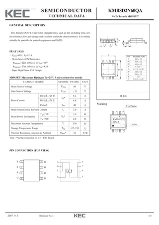
MOSFET Maximum Ratings (Ta=25 Unless otherwise noted)
B2
G
H
B1
1 4
58
A
PD L
T
FLP-8
0.20+0.1/-0.05T
P 1.27
MILLIMETERSDIM
A 4.85 0.2+_
B1 3.94 0.2+_
B2 6.02 0.3+_
D 0.4 0.1+_
G 0.15+0.1/-0.05
H 1.63 0.2+_
L 0.65 0.2+_
Note : *Surface Mounted on 1 1 FR4 Board
1
2
3
4
8
7
6
5
S
S
S
G
D
D
D
D
1
2
3
4
8
7
6
5
KMB8D2N
60QA
PIN CONNECTION (TOP VIEW)
CHARACTERISTIC SYMBOL PATING UNIT
Drain Source Voltage VDSS 60 V
Gate Source Voltage VGSS 25 V
Drain Current
DC@TA=25
ID*
8.2 A
DC@TA=70 6.6 A
Pulsed IDP 40 A
Drain Source Diode Forward Current IS 3.0 A
Drain Power Dissipation
TA=25
PD*
3.0 W
TA=70 2.0 W
Maximum Junction Temperature Tj 150
Storage Temperature Range Tstg -55~150
Thermal Resistance, Junction to Ambient RthJA* 41 /W
www.DataSheet4U.com
2. 2007. 9. 3 2/4
KMB8D2N60QA
Revision No : 1
ELECTRICAL CHARACTERISTICS (Ta=25 ) UNLESS OTHERWISE NOTED
CHARACTERISTIC SYMBOL TEST CONDITION MIN. TYP. MAX. UNIT
Static
Drain-Source Breakdown Voltage BVDSS VGS=0V, IDS=250 A 60 - - V
Drain Cut-off Current IDSS
VDS=48V, VGS=0V - - 1
A
VDS=48V, VGS=0V, Tj=70 - - 5
Gate Leakage Current IGSS VGS= 20V, VDS=0V - - 100 nA
Gate Threshold Voltage Vth VDS=VGS, ID=250 A 1.0 - 3.0 V
Drain-Source ON Resistance RDS(ON)*
VGS=10V, ID=8.2A - 16 22
m
VGS=4.5V, ID=7.6A - 20 27
Forward Transconductance Gfs* VDS=5V, ID=8.2A - 2.4 - S
Dynamic
Input Capaclitance Ciss
VDS=30V, VGS=0V, f=1MHz
- 1920 2300
pFOuput Capacitance Coss - 155 -
Reverse Transfer Capacitance Crss - 116 -
Total Gate Charge (VGS=10V)
Qg*
VDS=30V, VGS=10V, ID=8.2A
- 47.6 58
nC
Total Gate Charge (VGS=4.5V) - 24.2 30
Gate-Source Charge Qgs* - 6.0 -
Gate-Drain Charge Qgd* - 14.4 -
Turn-On Delay Time td(on)*
VDD=30V, VGS=10V
RL=3.6 , RG=3
- 8.2 -
ns
Turn-On Rise Time tr* - 5.5 -
Turn-On Delay Time td(off)* - 29.7 -
Turn-On Fall Time tf* - 5.2 -
Source-Drain Diode Ratings
Source-Drain Forward Voltage VSDF* VGS=0V, IDR=1.7A, - 0.74 1.0 V
Note
1. Pulse Test : Pulse width 10 , Duty cycle 1%
3. 2007. 9. 3 3/4
KMB8D2N60QA
Revision No : 1
0
0
4
10
20
30
40
8 12 16 20
VGS=4.0V
VGS=3.5V
VGS=4.5V
VGS=10V
VGS=5.5V
VGS=6V
VGS=8V, 10V
10
0
0
20
30
40
1 2 43 5
On-ResistanceRDS(ON)(mΩ)On-ResistanceRDS(ON)(mΩ)
0
10
30
60
50
20
40
0 125 150 17575 10050-25 25-50-75
Junction Temperature Tj ( )C
Junction Temperature Tj ( )C
GateThresholdVoltageVth(V)
Fig1. ID - VDS
DrainCurrentID(A)
DrainCurrentID(A)
Drain Current ID (A)Drain - Source Voltage VDS (V)
Fig3. ID - VGS
DrainCurrentID(A)
Gate Source Voltage VGS (V)
0
0
10
10
20
30
40
50
20 30 40 50
Fig2. RDS(ON) - ID
Fig4. RDS(ON) - Tj
Fig5. Vth - Tj
0.40
0
1.20.8 2.01.6
20
10
40
30
Fig 6. IS - VSDF
Source-Drain Forward Voltage VSDF
(V)
Common Source
Ta=25
Pulse Test
C
Common Source
Ta=25
Pulse Test
C
Common Source
VDS=5V
Pulse Test
Common Source
VGS=10V
Pulse Test
Common Source
VGS=VDS
ID=250µA
Pulse Test
Common Source
Ta=25
Pulse Test
C
25 C150 C
-55 C
0
1
3
5
2
4
0 125 150 17575 10050-25 25-50-75
4. 2007. 9. 3 4/4
KMB8D2N60QA
Revision No : 1
20100
0
40 5030
10
8
6
4
2
Fig7. VGS - Qg
GatetoSourceVoltageVGS(V)
Gate Charge Qg (nC)
VDS=30V
ID=8.2A
1050
0
20 25 3015
2500
2000
3500
3000
1500
1000
500
Fig8. C - VDS
CapacitanceC(pF)
Drain - Source Voltage VDS (V)
f=1MHz
DrainCurrentID(A)
Drain - Source Voltage VDS (V)
Fig9. Safe Operation Area
101
10
1
10
2
10
-2
10
-1
10-1
10-2
100
10
0
10
2
Operation in this
area is limited by RDS(ON)
1ms
10s
10ms
100ms
1s
DC
VGS=10V
SINGLE PULSE
TA = 25 C
100µs
Crss
Coss
Ciss
Fig10. Transient Thermal Response Curve
10-4 10-110-2 100 10 102 10310-3
10-1
10-2
100
10-3
Square Wave Pulse Duration (sec)
NormalizedEffectiveTransientThermalResistance
Rth(C/W)
0.1
0.01
0.02
0.05
0.2
0.5
SINGLE - Duty cycle D = t1/t2
t1
t2
PDM