Standard vs Custom Battery Packs - Decoding the Power Play
RT7257E Datasheet PDF
1. RT7257E
1
Preliminary
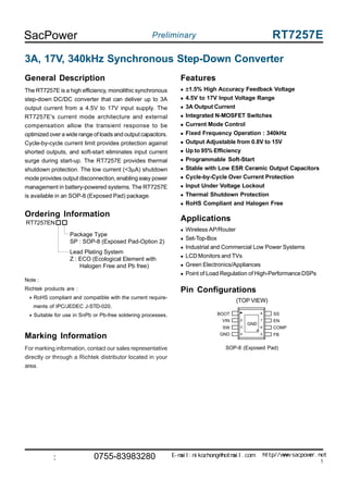
Ordering Information
Note :
Richtek products are :
RoHS compliant and compatible with the current require-
ments of IPC/JEDEC J-STD-020.
Suitable for use in SnPb or Pb-free soldering processes.
Pin Configurations
(TOP VIEW)
Applications
Wireless AP/Router
Set-Top-Box
Industrial and Commercial Low Power Systems
LCDMonitors and TVs
Green Electronics/Appliances
Point of Load Regulation of High-PerformanceDSPs
SOP-8 (Exposed Pad)
3A, 17V, 340kHz Synchronous Step-Down Converter
General Description
The RT7257E is a high efficiency, monolithic synchronous
step-down DC/DC converter that can deliver up to 3A
output current from a 4.5V to 17V input supply. The
RT7257E's current mode architecture and external
compensation allow the transient response to be
optimized over a wide range of loads and output capacitors.
Cycle-by-cycle current limit provides protection against
shorted outputs, and soft-start eliminates input current
surge during start-up. The RT7257E provides thermal
shutdown protection. The low current (<3μA) shutdown
mode provides output disconnection, enabling easy power
management in battery-powered systems. The RT7257E
is available in an SOP-8 (Exposed Pad) package.
Features
±±±±±1.5% High Accuracy Feedback Voltage
4.5V to 17V Input Voltage Range
3A Output Current
Integrated N-MOSFET Switches
Current Mode Control
Fixed Frequency Operation : 340kHz
Output Adjustable from 0.8V to 15V
Up to 95% Efficiency
Programmable Soft-Start
Stable with Low ESR Ceramic Output Capacitors
Cycle-by-Cycle Over Current Protection
Input Under Voltage Lockout
Thermal Shutdown Protection
RoHS Compliant and Halogen Free
BOOT
VIN
SW
GND
SS
EN
FB
COMP
GND
2
3
4 5
6
7
8
9
Marking Information
For marking information, contact our sales representative
directly or through a Richtek distributor located in your
area.
Package Type
SP : SOP-8 (Exposed Pad-Option 2)
RT7257EN
Lead Plating System
Z : ECO (Ecological Element with
Halogen Free and Pb free)
SacPower 智联创新
0755-83983280 E-mail:nikozhong@hotmail.com http//www.sacpower.net
联系人:钟先生
2. RT7257E
2
Preliminary
Functional Pin Description
Pin No. Pin Name Pin Function
1 BOOT
Bootstrap for High Side Gate Driver. Connect a 0.1μF or greater ceramic
capacitor from BOOT to SW pins.
2 VIN
Input Supply Voltage, 4.5V to 17V. Must bypass with a suitably large ceramic
capacitor.
3 SW Switch Node. Connect this pin to an external L-C filter.
4,
9 (Exposed Pad)
GND
Ground. The exposed pad must be soldered to a large PCB and connected to
GND for maximum power dissipation.
5 FB
Feedback Input. It is used to regulate the output of the converter to a set value
via an internal resistive voltage divider.
6 COMP
Compensation Node. COMP is used to compensate the regulation control
loop. Connect a series RC network from COMP to GND. In some cases, an
additional capacitor from COMP to GND is required.
7 EN
Enable Input. A logic high enables the converter; a logic low forces the
RT7257E into shutdown mode reducing the supply current to less than 3μA.
Attach this pin to VIN with a 100kΩ pull up resistor for automatic startup.
8 SS
Soft-Start Control Input. SS controls the soft-start period. Connect a capacitor
from SS to GND to set the soft-start period. A 0.1μF capacitor sets the
soft-start period to 13.5ms.
Typical Application Circuit
VOUT (V) R1 (kΩ) R2 (kΩ) RC (kΩ) CC (nF) L (μH) COUT (μF)
8 27 3 24 4.7 22 22 x 2
5 62 11.8 18 4.7 15 22 x 2
3.3 75 24 12 4.7 10 22 x 2
2.5 25.5 12 8.2 4.7 6.8 22 x 2
1.5 10.5 12 3.6 4.7 3.6 22 x 2
1.2 12 24 3 4.7 3.6 22 x 2
1 3 12 2.7 4.7 3.6 22 x 2
Table 1. Recommended Components Selection
VIN
EN
GND
BOOT
FB
SW
7
5
2
3
1
L
10µH100nF
22µF x 2
R1
75k
R2
24k
VOUT
3.3V
10µF x 2
VIN
4.5V to 17V
RT7257E
SS8
CSS
COMP
CC
4.7nF
RC
12k
CP
Open
64, 9 (Exposed Pad)
CBOOTCIN
0.1µF
COUT
Chip Enable
4. RT7257E
4
Preliminary
Electrical Characteristics
(VIN = 12V, TA = 25°C, unless otherwise specified)
Absolute Maximum Ratings (Note 1)
Supply Input Voltage, VIN ------------------------------------------------------------------------------------------ −0.3V to 20V
Switch Voltage, SW ------------------------------------------------------------------------------------------------ −0.3V to (VIN + 0.3V)
VBOOT − VSW ---------------------------------------------------------------------------------------------------------- −0.3V to 6V
Other Pins Voltage ------------------------------------------------------------------------------------------------- −0.3V to 20V
Power Dissipation, PD @ TA = 25°C
SOP-8 (Exposed Pad) --------------------------------------------------------------------------------------------- 1.333W
Package Thermal Resistance (Note 2)
SOP-8 (Exposed Pad), θJA ---------------------------------------------------------------------------------------- 75°C/W
SOP-8 (Exposed Pad), θJC --------------------------------------------------------------------------------------- 15°C/W
Lead Temperature (Soldering, 10 sec.)------------------------------------------------------------------------- 260°C
Junction Temperature ----------------------------------------------------------------------------------------------- 150°C
Storage Temperature Range -------------------------------------------------------------------------------------- −65°C to 150°C
ESD Susceptibility (Note 3)
HBM (Human Body Mode) ---------------------------------------------------------------------------------------- 2kV
MM (Machine Mode) ------------------------------------------------------------------------------------------------ 200V
Recommended Operating Conditions (Note 4)
Supply Input Voltage, VIN ------------------------------------------------------------------------------------------ 4.5V to 17V
Junction Temperature Range-------------------------------------------------------------------------------------- −40°C to 125°C
Ambient Temperature Range-------------------------------------------------------------------------------------- −40°C to 85°C
Parameter Symbol Test Conditions Min Typ Max Unit
Shutdown Supply Current VEN = 0V -- 0.5 3 μA
Supply Current VEN = 3 V, VFB = 0.9V -- 0.8 1.2 mA
Feedback Voltage VFB 4.5V ≤ VIN ≤ 17V 0.788 0.8 0.812 V
Error Amplifier
Transconductance
GEA ΔIC = ±10μA -- 940 -- μA/V
High Side Switch
On-Resistance
RDS(ON)1 -- 110 -- mΩ
Low Side Switch
On-Resistance
RDS(ON)2 -- 90 -- mΩ
High Side Switch Leakage
Current
VEN = 0V, VSW = 0V -- 0 10 μA
Upper Switch Current Limit Min. Duty Cycle, VBOOT − VSW = 4.8V -- 5.1 -- A
COMP to Current Sense
Transconductance
GCS -- 4.7 -- A/V
Oscillation Frequency fOSC1 300 340 380 kHz
Short Circuit Oscillation
Frequency
fOSC2 VFB = 0V -- 100 -- kHz
Maximum Duty Cycle DMAX VFB = 0.7V -- 93 -- %
Minimum On Time tON -- 100 -- ns
To be continued
5. RT7257E
5
Preliminary
Parameter Symbol Test Conditions Min Typ Max Unit
Logic-High VIH 2 -- 5.5EN Input Threshold
Voltage Logic-Low VIL -- -- 0.4
V
Input Under Voltage Lockout Threshold VUVLO VIN Rising 3.8 4.2 4.5 V
Input Under Voltage Lockout Hysteresis ΔVUVLO -- 320 -- mV
Soft-Start Current ISS VSS = 0V -- 6 -- μA
Soft-Start Period tSS CSS = 0.1μF -- 13.5 -- ms
Thermal Shutdown TSD -- 150 -- °C
Note 1. Stresses listed as the above "Absolute Maximum Ratings" may cause permanent damage to the device. These are for
stress ratings. Functional operation of the device at these or any other conditions beyond those indicated in the
operational sections of the specifications is not implied. Exposure to absolute maximum rating conditions for extended
periods may remain possibility to affect device reliability.
Note 2. θJA is measured in natural convection at TA = 25°C on a high effective thermal conductivity four-layer test board of
JEDEC 51-7 thermal measurement standard. The measurement case position of θJC is on the exposed pad of the
package.
Note 3. Devices are ESD sensitive. Handling precaution is recommended.
Note 4. The device is not guaranteed to function outside its operating conditions.
6. RT7257E
6
Preliminary
Typical Operating Characteristics
Reference Voltage vs. Temperature
0.780
0.785
0.790
0.795
0.800
0.805
0.810
0.815
0.820
-50 -25 0 25 50 75 100 125
Temperature (°C)
ReferenceVoltage(V)
VIN = 12V, VOUT = 3.3V, IOUT = 1A
Output Voltage vs. Load Current
3.250
3.276
3.302
3.328
3.354
3.380
0 0.5 1 1.5 2 2.5 3
Load Current (A)
OutputVoltage(V)
VOUT = 3.3V
VIN = 4.5V
VIN = 12V
VIN = 17V
Reference Voltage vs. Input Voltage
0.780
0.785
0.790
0.795
0.800
0.805
0.810
0.815
0.820
4.5 7 9.5 12 14.5 17
Input Voltage (V)
ReferenceVoltage(V)
VIN = 4.5V to 17V, VOUT = 3.3V, IOUT = 1A
Switching Frequency vs. Temperature
300
310
320
330
340
350
360
370
-50 -25 0 25 50 75 100 125
Temperature (°C)
SwitchingFrequency(kHz)1
VIN = 12V, VOUT = 3.3V, IOUT = 0.5A
Switching Frequency vs. Input Voltage
300
310
320
330
340
350
360
370
380
4.5 7 9.5 12 14.5 17
Input Voltage (V)
SwitchingFrequency(kHz)1
VOUT = 3.3V, IOUT = 0.3A
Efficiency vs. Load Current
0
10
20
30
40
50
60
70
80
90
100
0.01 0.1 1 10
Load Current (A)
Efficiency(%)
VOUT = 3.3V
VIN = 4.5V
VIN = 12V
VIN = 17V
7. RT7257E
7
Preliminary
Current Limit vs. Temperature
2
3
4
5
6
7
8
-50 -25 0 25 50 75 100 125
Temperature (°C)
CurrentLimit(A)
VIN = 12V, VOUT = 3.3V
Time (5ms/Div)
Power On from VIN
VOUT
(2V/Div)
VIN
(5V/Div)
IL
(2A/Div)
VIN = 12V, VOUT = 3.3V, IOUT = 3A
Time (5ms/Div)
Power Off from VIN
VOUT
(2V/Div)
VIN
(5V/Div)
IL
(2A/Div)
VIN = 12V, VOUT = 3.3V, IOUT = 3A
Time (250μs/Div)
Load Transient Response
VOUT
(100mV/Div)
IOUT
(2A/Div)
VIN = 12V, VOUT = 3.3V, IOUT = 0.2A to 3A
Time (250μs/Div)
Load Transient Response
VOUT
(100mV/Div)
IOUT
(2V/Div)
VIN = 12V, VOUT = 3.3V, IOUT = 1.5A to 3A
Time (1μs/Div)
Switching
VOUT
(10mV/Div)
VSW
(10V/Div)
IL
(2A/Div) VIN = 12V, VOUT = 3.3V, IOUT = 3A
8. RT7257E
8
Preliminary
Time (5ms/Div)
Power On from EN
VOUT
(2V/Div)
VEN
(5V/Div)
IL
(2A/Div)
VIN = 12V, VOUT = 3.3V, IOUT = 2A
Time (5ms/Div)
Power Off from EN
VOUT
(2V/Div)
VEN
(5V/Div)
IL
(2A/Div)
VIN = 12V, VOUT = 3.3V, IOUT = 2A
9. RT7257E
9
Preliminary
Application Information
The RT7257E is a synchronous high voltage buck converter
that can support the input voltage range from 4.5V to 17V
and the output current can be up to 3A.
Output Voltage Setting
The resistive divider allows the FB pin to sense the output
voltage as shown in Figure 1.
Figure 1. Output Voltage Setting
The output voltage is set by an external resistive voltage
divider according to the following equation :
⎛ ⎞+⎜ ⎟
⎝ ⎠
OUT FB
R1V = V 1
R2
Where VFB is the feedback reference voltage (0.8V typ.).
External Bootstrap Diode
Connect a 100nF low ESR ceramic capacitor between
the BOOT pin and SW pin. This capacitor provides the
gate driver voltage for the high side MOSFET.
It is recommended to add an external bootstrap diode
between an external 5V and BOOT pin for efficiency
improvement when input voltage is lower than 5.5V or duty
ratio is higher than 65% .The bootstrap diode can be a
low cost one such as IN4148 or BAT54. The external 5V
can be a 5V fixed input from system or a 5V output of the
RT7257E. Note that the external boot voltage must be
lower than 5.5V
Figure 2. External Bootstrap Diode
Soft-Start
The RT7257E contains an external soft-start clamp that
gradually raises the output voltage. The soft-start timing
can be programmed by the external capacitor between
SS pin and GND. The chip provides a 6μAcharge current
for the external capacitor. If 0.1μF capacitor is used to
set the soft-start, it's period will be 13.5ms (typ.).
Chip Enable Operation
The EN pin is the chip enable input. Pulling the EN pin
low (<0.4V) will shutdown the device. During shutdown
mode, the RT7257E quiescent current drops to lower than
3μA. Driving the EN pin high (>2V, < 17V) will turn on the
device again. For external timing control (e.g.RC), the EN
pin can also be externally pulled high by adding a REN*
resistor and CEN* capacitor from the VIN pin (see Figure
5).
An external MOSFET can be added to implement digital
control on the EN pin when no system voltage above 2V
is available, as shown in Figure 3. In this case, a 100kΩ
pull-up resistor, REN, is connected between VIN and the
EN pin. MOSFET Q1 will be under logic control to pull
down the EN pin.
Figure 3. Enable Control Circuit for Logic Control with
Low Voltage
To prevent enabling circuit when VIN is smaller than the
VOUT target value, a resistive voltage divider can be placed
between the input voltage and ground and connected to
the EN pin to adjust IC lockout threshold, as shown in
Figure 4. For example, if an 8V output voltage is regulated
from a 12V input voltage, the resistor REN2 can be selected
to set input lockout threshold larger than 8V.
RT7257E
GND
FB
R1
R2
VOUT
SW
BOOT
5V
RT7257E 100nF
VIN
EN
GND
BOOT
FB
SW7
5
2
3
1
L
R1
R2
VOUT
Chip Enable
VIN
RT7257E
SS8
CSS
COMP
CC RC
CP
6
CBOOT
COUT
CIN
REN
Q1
100k
4,
9 (Exposed Pad)
10. RT7257E
10
Preliminary
OUT OUT
L
IN
V V
I = 1
f L V
⎡ ⎤ ⎡ ⎤Δ × −⎢ ⎥ ⎢ ⎥×⎣ ⎦ ⎣ ⎦
Inductor Selection
The inductor value and operating frequency determine the
ripple current according to a specific input and output
voltage. The ripple current ΔIL increases with higher VIN
and decreases with higher inductance.
Figure 4. The Resistors can be Selected to Set IC
Lockout Threshold
Having a lower ripple current reduces not only the ESR
losses in the output capacitors but also the output voltage
ripple. High frequency with small ripple current can achieve
the highest efficiency operation. However, it requires a
large inductor to achieve this goal.
For the ripple current selection, the value of ΔIL= 0.24(IMAX)
will be a reasonable starting point. The largest ripple
current occurs at the highest VIN. To guarantee that the
ripple current stays below the specified maximum, the
inductor value should be chosen according to the following
equation :
OUT IN
RMS OUT(MAX)
IN OUT
V V
I = I 1
V V
−
CIN and COUT Selection
The input capacitance, CIN, is needed to filter the
trapezoidal current at the source of the high side MOSFET.
To prevent large ripple current, a low ESR input capacitor
sized for the maximum RMS current should be used. The
RMS current is given by :
Table 2. Suggested Inductors for Typical
Application Circuit
Component
Supplier
Series
Dimensions
(mm)
TDK VLF10045 10 x 9.7 x 4.5
TDK SLF12565 12.5 x 12.5 x 6.5
TAIYO
YUDEN
NR8040 8 x 8 x 4
OUT OUT
L(MAX) IN(MAX)
V V
L = 1
f I V
⎡ ⎤ ⎡ ⎤
× −⎢ ⎥ ⎢ ⎥× Δ⎣ ⎦ ⎣ ⎦
The inductor's current rating (caused a 40°C temperature
rising from 25°C ambient) should be greater than the
maximum load current and its saturation current should
be greater than the short circuit peak current limit. Please
see Table 2 for the inductor selection reference.
This formula has a maximum at VIN = 2VOUT, where
IRMS = IOUT / 2. This simple worst case condition is
commonly used for design because even significant
deviations do not offer much relief.
Choose a capacitor rated at a higher temperature than
required. Several capacitors may also be paralleled to
meet size or height requirements in the design.
For the input capacitor, two 10μF low ESR ceramic
capacitors are recommended. For the recommended
capacitor, please refer to Table 3 for more details.
The selection of COUT is determined by the required ESR
to minimize voltage ripple.
Moreover, the amount of bulk capacitance is also a key
for COUT selection to ensure that the control loop is stable.
Loop stability can be checked by viewing the load transient
response as described in a later section.
The output ripple, ΔVOUT , is determined by :
OUT L
OUT
1V I ESR
8fC
⎡ ⎤Δ ≤ Δ +⎢ ⎥⎣ ⎦
VIN
EN
GND
BOOT
FB
SW7
5
2
3
1
L
R1
R2
VOUT
VIN
RT7257E
SS8
CSS
COMP
CC RC
CP
6
CBOOT
COUT
CIN
100k
8V
12V
REN2
REN1 10µF x 2
4,
9 (Exposed Pad)
11. RT7257E
11
Preliminary
The output ripple will be the highest at the maximum input
voltage since ΔIL increases with input voltage. Multiple
capacitors placed in parallel may be needed to meet the
ESR and RMS current handling requirement. Higher values,
lower cost ceramic capacitors are now becoming available
in smaller case sizes. Their high ripple current, high voltage
rating and low ESR make them ideal for switching regulator
applications. However, care must be taken when these
capacitors are used at input and output. When a ceramic
capacitor is used at the input and the power is supplied
by a wall adapter through long wires, a load step at the
output can induce ringing at the input, VIN. At best, this
ringing can couple to the output and be mistaken as loop
instability. At worst, a sudden inrush of current through
the long wires can potentially cause a voltage spike at
VIN large enough to damage the part.
EMI Consideration
Since parasitic inductance and capacitance effects in PCB
circuitry would cause a spike voltage on SW pin when
high side MOSFET is turned-on/off, this spike voltage on
SW may impact on EMI performance in the system. In
order to enhance EMI performance, there are two methods
to suppress the spike voltage. One is to place an R-C
snubber between SW and GND and make them as close
as possible to the SW pin (see Figure 5). Another method
is adding a resistor in series with the bootstrap
capacitor, CBOOT. But this method will decrease the driving
capability to the high side MOSFET. It is strongly
recommended to reserve the R-C snubber during PCB
layout for EMI improvement. Moreover, reducing the SW
trace area and keeping the main power in a small loop will
be helpful on EMI performance. For detailed PCB layout
guide, please refer to the section of Layout Consideration.
Figure 5. Reference Circuit with Snubber and Enable Timing Control
Thermal Considerations
For continuous operation, do not exceed the maximum
operation junction temperature 125°C. The maximum
power dissipation depends on the thermal resistance of
IC package, PCB layout, the rate of surroundings airflow
and temperature difference between junction to ambient.
The maximum power dissipation can be calculated by
following formula :
PD(MAX) = (TJ(MAX) − TA) / θJA
Where TJ(MAX) is the maximum operation junction
temperature , TA is the ambient temperature and the θJA is
the junction to ambient thermal resistance.
For recommended operating conditions specification of
RT7257E, the maximum junction temperature is 125°C.
The junction to ambient thermal resistance θJA is layout
dependent. For SOP-8 (Exposed Pad) package, the
thermal resistance θJA is 75°C/W on the standard JEDEC
51-7 four-layers thermal test board. The maximum power
dissipation at TA = 25°C can be calculated by following
formula :
PD(MAX) = (125°C − 25°C) / (75°C/W) = 1.333W
(min.copper area PCB layout)
PD(MAX) = (125°C − 25°C) / (49°C/W) = 2.04W
(70mm2
copper area PCB layout)
VIN
EN
GND
BOOT
FB
SW
7
5
2
3
1
L
10µH100nF
22µFx2
R1
75k
R2
24k
VOUT
3.3V/3A
10µF x 2
Chip Enable
VIN
4.5V to 17V
RT7257E
SS8
CSS
0.1µF
COMP
CC
4.7nF
RC
12k
CP
NC
6
4,
9 (Exposed Pad)
CBOOT
COUT
CIN
RBOOT*
RS*
CS*
REN*
CEN*
* : Optional
12. RT7257E
12
Preliminary
The thermal resistance θJA of SOP-8 (Exposed Pad) is
determined by the package architecture design and the
PCB layout design. However, the package architecture
design had been designed. If possible, it's useful to
increase thermal performance by the PCB layout copper
design. The thermal resistance θJA can be decreased by
adding copper area under the exposed pad of SOP-8
(Exposed Pad) package.
As shown in Figure 6, the amount of copper area to which
the SOP-8 (Exposed Pad) is mounted affects thermal
performance. When mounted to the standard
SOP-8 (Exposed Pad) pad (Figure 6.a), θJA is 75°C/W.
Adding copper area of pad under the SOP-8 (Exposed
Pad) (Figure 6.b) reduces the θJA to 64°C/W. Even further,
increasing the copper area of pad to 70mm2
(Figure 6.e)
reduces the θJA to 49°C/W.
The maximum power dissipation depends on operating
ambient temperature for fixed TJ(MAX) and thermal
resistance θJA. For RT7257E packages, the Figure 7 of
derating curves allows the designer to see the effect of
rising ambient temperature on the maximum power
dissipation allowed.
Figure 7.Derating Curves for RT7257E Package
0.0
0.2
0.4
0.6
0.8
1.0
1.2
1.4
1.6
1.8
2.0
2.2
0 25 50 75 100 125
Ambient Temperature (°C)
PowerDissipation(W)
Copper Area
70mm2
50mm2
30mm2
10mm2
Min.Layout
Four-Layer PCB
(a) Copper Area = (2.3 x 2.3) mm2
, θJA = 75°C/W
(b) Copper Area = 10mm2
,θJA = 64°C/W
(c) Copper Area = 30mm2
, θJA = 54°C/W
(d) Copper Area = 50mm2
,θJA = 51°C/W
(e) Copper Area = 70mm2
,θJA = 49°C/W
Figure 6. Themal Resistance vs. Copper Area Layout
Design
13. RT7257E
13
Preliminary
Layout Consideration
Follow the PCB layout guidelines for optimal performance
of the RT7257E.
Keep the traces of the main current paths as short and
wide as possible.
Put the input capacitor as close as possible to the device
pins (VINandGND).
SW node is with high frequency voltage swing and
should be kept at small area. Keep analog components
away from the SW node to prevent stray capacitive noise
pick-up.
Figure 8. PCB Layout Guide
Table 3. Suggested Capacitors for CIN and COUT
Location Component Supplier Part No. Capacitance (μF) Case Size
CIN MURATA GRM31CR61E106K 10 1206
CIN TDK C3225X5R1E106K 10 1206
CIN TAIYO YUDEN TMK316BJ106ML 10 1206
COUT MURATA GRM31CR60J476M 47 1206
COUT TDK C3225X5R0J476M 47 1210
COUT MURATA GRM32ER71C226M 22 1210
COUT TDK C3225X5R1C22M 22 1210
VIN
VOUT
GND
CIN
GND
CP
CC
RC
SW
VOUT
COUT
L
R1
R2
Input capacitor must
be placed as close
to the IC as possible.
SW nods is with high frequency voltage swing and should
be kept at small area. Keep analog components away from
the SW node to prevent stray capacitive noise pick-up
The feedback components
must be connected as close
to the device as possible.
BOOT
VIN
SW
GND
SS
EN
FB
COMP
GND
2
3
4 5
6
7
8
9
CSS
RS*
CS*
GND VIN
RENCBOOT
Connect feedback network behind the output capacitors.
Keep the loop area small. Place the feedback
components near the RT7257E.
Connect all analog grounds to a command node and
then connect the command node to the power ground
behind the output capacitors.
An example of PCB layout guide is shown in Figure 8
for reference.
14. RT7257E
14
Preliminary
Outline Dimension
A
BJ
F
H
M
C
D
I
Y
X
EXPOSED THERMAL PAD
(Bottom of Package)
8-Lead SOP (Exposed Pad) Plastic Package
Dimensions In Millimeters Dimensions In Inches
Symbol
Min Max Min Max
A 4.801 5.004 0.189 0.197
B 3.810 4.000 0.150 0.157
C 1.346 1.753 0.053 0.069
D 0.330 0.510 0.013 0.020
F 1.194 1.346 0.047 0.053
H 0.170 0.254 0.007 0.010
I 0.000 0.152 0.000 0.006
J 5.791 6.200 0.228 0.244
M 0.406 1.270 0.016 0.050
X 2.000 2.300 0.079 0.091
Option 1
Y 2.000 2.300 0.079 0.091
X 2.100 2.500 0.083 0.098
Option 2
Y 3.000 3.500 0.118 0.138