Vlsi design and fabrication ppt
•Télécharger en tant que PPT, PDF•
9 j'aime•14,283 vues


Recommandé
Contenu connexe
Tendances
Tendances (20)
En vedette
En vedette (20)
Similaire à Vlsi design and fabrication ppt
Similaire à Vlsi design and fabrication ppt (20)
Plus de Manjushree Mashal
Plus de Manjushree Mashal (16)
Vlsi design and fabrication ppt
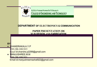
- 1. DEPARTMENT OF ELECTRONICS & COMMUNICATION PAPER PRESENTATION ON VLSI DESIGN AND FABRICATION BY: ● CHANDRAKALA.Y.P USN:2BL10EC015 Email id:chandra.p2299@gmail.com ● MANJUSHREE.M.M USN:2BL10EC031 Email id:manjushreemashal922@gmail.com
- 3. Outline Introduction Silicon, p n-junctions and transistors A Brief History Operation of MOS Transistors CMOS circuits Fabrication
- 4. Introduction Integrated circuits: many transistors on one chip. Very Large Scale Integration (VLSI) Complementary Metal Oxide Semiconductor (CMOS) Fast, cheap, “low-power” transistors circuits
- 5. Why VLSI? Integration improves the design Lower parasitics = higher speed Lower power consumption Physically smaller Integration reduces manufacturing cost - (almost) no manual assembly
- 6. WHY VLSI DESIGN? Money, technology, civilization
- 7. Annual Sales 1018 transistors manufactured in 2003 100 million for every human on the planet 0 50 100 150 200 1982 1984 1986 1988 1990 1992 1994 1996 1998 2000 2002 Year GlobalSemiconductorBillings (BillionsofUS$)
- 8. MOS Transistors Four terminal device: gate, source, drain, body Gate – oxide – body stack looks like a capacitor Gate and body are conductors (body is also called the substrate) SiO2 (oxide) is a “good” insulator (separates the gate from the body Called metal–oxide–semiconductor (MOS) capacitor, even though gate is mostly made of poly-crystalline silicon (polysilicon) n+ p GateSource Drain bulk Si SiO2 Polysilicon n+ SiO2 n GateSource Drain bulk Si Polysilicon p+ p+ NMOS PMOS
- 9. Body is commonly tied to ground (0 V) Drain is at a higher voltage than Source When the gate is at a low voltage: P-type body is at low voltage Source-body and drain-body “diodes” are OFF No current flows, transistor is OFF n+ p GateSource Drain bulk Si SiO2 Polysilicon n+ D 0 S NMOS Operation
- 10. NMOS Operation Cont. When the gate is at a high voltage: Positive charge on gate of MOS capacitor Negative charge is attracted to body under the gate Inverts a channel under gate to “n-type” (N-channel, hence called the NMOS) if the gate voltage is above a threshold voltage (VT) Now current can flow through “n-type” silicon from source through channel to drain, transistor is ON n+ p GateSource Drain bulk Si SiO2 Polysilicon n+ D 1 S
- 11. PMOS Transistor Similar, but doping and voltages reversed Body tied to high voltage (VDD) Drain is at a lower voltage than the Source Gate low: transistor ON Gate high: transistor OFF Bubble indicates inverted behavior SiO2 n GateSource Drain bulk Si Polysilicon p+ p+
- 12. Physical Layout Chips are specified with set of masks Minimum dimensions of masks determine transistor size (and hence speed, cost, and power) Feature size f = distance between source and drain Set by minimum width of polysilicon Feature size improves 30% every 3 years or so Normalize for feature size when describing design rules Express rules in terms of = f/2 E.g. = 0.3 m in 0.6 m process
- 13. Simplified Design Rules Conservative rules to get you started
- 14. http://public.itrs.net/Files/2003ITRS/Home2003.htm The Future? International Technology Roadmap for Semiconductors
- 15. Summary MOS Transistors are stack of gate, oxide, silicon and p-n junctions Can be viewed as electrically controlled switches Build logic gates out of switches Draw masks to specify layout of transistors Now you know everything necessary to start designing schematics and layout for a simple chip!
- 17. Organization �Materials Used in VLSI Fabrication �VLSI Fabrication Technologies �Overview of Fabrication Methods
- 18. 3 Main Categories of Materials Materials can be classified into three main Groups regarding their electrical conduction properties: �Insulators �Conductors �Semiconductors
- 19. 4 Conductors Conductors are used in IC design for electrical connectivity. The following are good conducting elements: �Silver �Gold �Copper �Aluminum �Platinum
- 20. 5 Insulators Insulators are use toisolate conductingand/or semi-conductingmaterialsfromeachother. MOS devicesand Capacitorsrelyon an insulatorfortheirphysicaloperation. The choiceof the insulators(and the conductors) in IC design dependsheavilyon howthe materials interactwitheachother, especiallywiththe semiconductors.
- 21. 6 Semiconductors �The basic semiconductor material usedin devicefabricationisSilicon �The success of thismaterial isdue to: �Phisicalcharacteristics �Abundance in nature and very low cost �Relatively easy process �Reliable high volume fabrication �Othersemiconductors(e.g. GaAs) are usedforspecial applications
- 22. Organization �MaterialsUsedin VLSI Fabrication �VLSI FabricationTechnologies �Overviewof FabricationMethods �Devicesimulation
- 23. 8 Overviewof Processing Technologies Althougha numberof processing technologiesare available, the majority of the production isdone withtraditionalCMOS. Otherprocessesare limited toareaswhereCMOS isnotverysuitable (likehigh speedRF applications)Bipolar:2%SOI: 1%GaAs: 2%CMOS: 90%BiCMOS: 5%
- 24. 9 CMOS technology �An Integrated Circuit (IC)is an electronic network fabricated in a single piece of a semiconductor material �The semiconductor surface is subjected to various processing steps in which impurities and other materials are added with specific geometrical patterns �The fabrication steps are sequenced to form three dimensional regions that act as transistors and interconnects that form the network
- 25. Simplified View of MOSFET
- 26. 11 CMOS Process The CMOS processallowsfabricationof nMOS and pMOStransistorsside-by-sideon the same Siliconsubstrate.
- 27. 12 Organization �Materials Used in VLSI Fabrication �VLSI FabricationTechnologies �Overviewof FabricationMethods �Devicesimulation
- 28. 13 Fabrication process sequence �Silicon manifacture �Wafer processing �Lithography �Oxide growth and removal �Diffusion and ion implantation �Annealing �Silicon deposition �Metallization �Testing �Assembly and packaging
- 29. 14 Single CrystalGrowth(I) �Pure siliconismeltedin a pot (1400º C) and a smallseedcontainingthe desiredcrystalorientationisinsertedintomoltensilicon and slowly(1mm/minute) pulledout.
- 30. 15 Single CrystalGrowth(II) �The siliconcrystal(in some casesalsocontainingdoping) ismanufacturedasa cylinder(ingot) witha diameterof 8-12 inches(1”=2.54cm). �Thiscylinderiscarefullysawedintothin(0.50-0.75 mm thick) diskscalledwafers, whichare laterpolishedand markedforcrystalorientation.
- 31. 16 Lithography(I) Lithography sequence steps: �Designer: �Drawing the “layer” patterns on a layout editor �Silicon Foundry: �Masks generation from the layer patterns in the design data base �Printing: transfer the mask pattern to the wafer surface �Process the wafer to physically pattern each layer of the IC Lithography: process used to transfer patterns to each layer of the IC
- 32. 17 Lithography(II) 1.Photoresistapplication: �the surface to be patterned is spin-coated with a light-sensitive organic polymer called photoresist 2.Printing (exposure): �the mask pattern is developed on the photoresist, with UV light exposure �depending on the type of photoresist(negative or positive), the exposed or unexposed parts become resistant to certain types of solvents 3.Development: �the soluble photoresistis chemically removed �The developed photoresistacts as a mask for patterning of underlying layers and then is removed.1. Photoresist coatingSiO2PhotoresistSubstrate3. DevelopmentSubstrateSubstrateMaskUltra violet
- 33. 18 OxideGrowth/ OxideDeposition �Oxide can be grownfrom silicon through heating in an oxidizing atmosphere �Gate oxide, device isolation �Oxidation consumes silicon �SiO2is depositedon materials other than silicon through reaction between gaseous silicon compounds and oxidizers �Insulation between different layers of metallizationXFOX0.54 XFOX0.46 XFOXSilicon waferSilicon surfaceField oxide
- 34. 19 Etching �Once the desired shape is patterned with photoresist, the etching process allows unprotected materials to be removed �Wet etching: uses chemicals �Dry or plasma etching: uses ionized gases
- 35. 20 Diffusionand IonImplantation Doping materialsare addedto changethe electricalcharacteristics of siliconlocallythrough: �Diffusion: dopantsdeposited on silicon move through the lattice by thermal diffusion (high temperature process) �Wells �Ion implantation: highly energized donor or acceptor atoms impinge on the surface and travel below it �The patterned SiO2serves as an implantation mask �Source and Drain regions
- 36. 21 Annealing Thermal annealingis a high temperature process which: �allows doping impurities to diffuse further into the bulk �repairs lattice damage caused by the collisions with doping ions
- 37. 22 Silicon Deposition and Metallization �Films of silicon can be added on the surface of a wafer �Epitaxy: growthof a single-crystal semiconductor film on a crystalline substate �Polysilicon: polycrystalline film with a granular structure obtained through depositionof silicon on an amorphous material �MOSFET gates �Metallization: deposition of metal layers by evaporation �interconnections
- 38. Advanced CMOS processes �Shallow trench isolation �source-drain halos (series resistance) �Self-aligned silicide(spacers) �…