Unit 4 dica
•Télécharger en tant que PPT, PDF•
4 j'aime•3,018 vues

Brief about computational logic design for ic

Recommandé
Contenu connexe
Tendances
Tendances (20)
Similaire à Unit 4 dica
Similaire à Unit 4 dica (20)
Dernier
Dernier (20)
Unit 4 dica
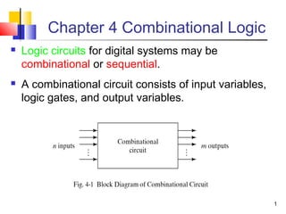
- 1. 1 Chapter 4 Combinational Logic Logic circuits for digital systems may be combinational or sequential. A combinational circuit consists of input variables, logic gates, and output variables.
- 2. Combinational Logic Design It is a process with 5 steps : 2 Specification Formulation Optimization Technology mapping Verification
- 3. 3 4-2. Analysis procedure To obtain the output Boolean functions from a logic diagram, proceed as follows: 1. Label all gate outputs that are a function of input variables with arbitrary symbols. Determine the Boolean functions for each gate output. 2. Label the gates that are a function of input variables and previously labeled gates with other arbitrary symbols. Find the Boolean functions for these gates.
- 4. 4 4-2. Analysis procedure 3. Repeat the process outlined in step 2 until the outputs of the circuit are obtained. 4. By repeated substitution of previously defined functions, obtain the output Boolean functions in terms of input variables.
- 5. 5 Example F2 = AB + AC + BC; T1 = A + B + C; T2 = ABC; T3 = F2’T1; F1 = T3 + T2 F1 = T3 + T2 = F2’T1 + ABC = A’BC’ + A’B’C + AB’C’ + ABC
- 6. 6 Derive truth table from logic diagram We can derive the truth table in Table 4-1 by using the circuit of Fig.4-2.
- 7. 7 4-3. Design procedure 1. Table4-2 is a Code-Conversion example, first, we can list the relation of the BCD and Excess-3 codes in the truth table.
- 8. 8 Karnaugh map 2. For each symbol of the Excess-3 code, we use 1’s to draw the map for simplifying Boolean function.
- 9. 9 Circuit implementation z = D’;y = CD + C’D’ = CD + (C + D)’ x = B’C + B’D + BC’D’ = B’(C + D) + B(C + D)’ w = A + BC + BD = A + B(C + D)
- 10. 10 4-4. Binary Adder-Subtractor A combinational circuit that performs the addition of two bits is called a half adder. The truth table for the half adder is listed below: S = x’y + xy’ C = xy S: Sum C: Carry
- 12. 12 Full-Adder One that performs the addition of three bits(two significant bits and a previous carry) is a full adder.
- 13. 13 Simplified Expressions S = x’y’z + x’yz’ + xy’z’ + xyz C = xy + xz + yz C
- 14. 14 Full adder implemented in SOP
- 15. 15 Another implementation Full-adder can also implemented with two half adders and one OR gate (Carry Look-Ahead adder). S = z ⊕ (x ⊕ y) = z’(xy’ + x’y) + z(xy’ + x’y)’ = xy’z’ + x’yz’ + xyz + x’y’z C = z(xy’ + x’y) + xy = xy’z + x’yz + xy
- 16. 16 Binary adder This is also called Ripple Carry Adder ,because of the construction with full adders are connected in cascade.
- 17. 17 Carry Propagation (Carry Look Ahead) Fig.4-9 causes a unstable factor on carry bit, and produces a longest propagation delay. The signal from Ci to the output carry Ci+1, propagates through an AND and OR gates, so, for an n-bit RCA, there are 2n gate levels for the carry to propagate from input to output.
- 18. 18 Carry Propagation (Carry Look Ahead) Because the propagation delay will affect the output signals on different time, so the signals are given enough time to get the precise and stable outputs. The most widely used technique employs the principle of carry look-ahead to improve the speed of the algorithm. Pi : carry propagate (0,1 & 1,0) Gi : carry generate (0,0 & 1,1)
- 19. 19 Boolean functions Pi = Ai ⊕ Bi Gi = AiBi Output sum and carry Si = Pi ⊕ Ci Ci+1 = Gi + PiCi Gi : carry generate ; Pi : carry propagate when i=0, C1 = G0 + P0C0 --------- (1) when i=1, C2 = G1 + P1C1 = G1 + P1G0 + P1P0C0 according to (1) -------- (2) when i=2, C3 = G2 + P2C2 = G2 + P2G1 + P2P1G0 + P2P1P0C0 according to (2) C3 does not have to wait for C2 and C1 to propagate.
- 20. 20 Logic diagram of carry look-ahead generator C3 is propagated at the same time as C2 and C1. =G0 + P0C0 G0 P0C0 = G1 + P1G0 + P1P0C0 G1P1G0 P1P0C0 = G2 + P2G1 + P2P1G0 + P2P1P0C0 G2 P2G1 P2P1G0 P2P1P0C0
- 21. 21 4-bit Parallel adder with carry look ahead Delay time of n-bit CLAA = XOR + (AND + OR) + XOR
- 22. 4 bit parallel adder using IC 74182 22
- 23. n-Bit Parallel Subtractor 23 In general subtraction, we made as A-B. Means A+(-B). We can write it as 2’s Complement of B is added to the A. 2’s complement means 1’s complement + 1. We make add inverter across B and take as carry 1. then it will also acts as 2’s complement of B. Then we make add that to A, by using adder circuit.
- 24. 24 Binary subtractor and adder selection in one design M = 1subtractor ; M = 0adder B0 XOR M (B0 XOR M) + A0 + C0 = 0
- 25. Spreadsheet/ Datasheet/ CARRY LOOK AHEAD 74182.pdf 25
- 26. 26
- 27. ALU A very popular & widely used combinational circuit is ALU which is capable of performing arithmetic as well as logical operation. Arithmetic Operating Modes: Addition Subtraction Shift Operation Magnitude Comparison 12 other arithmetic operations 27
- 28. Logical Operating Modes: Exclusive OR Comparator AND, NAND, OR, NOR 10 other arithmetic operations 28
- 29. 1/8/2012 - L3 Data Path Design Copyright 2006 - Joanne DeGroat, ECE, OSU 29 ALU Operations (integer ALU) Add (A+B) Add with Carry (A+B+Cin) Subtract (A-B) Subtract with Borrow (A-B-Cin) [Subract reverse (B-A)] [Subract reverse with Borrow (B-A- Cin)] Negative A (-A) Negative B (-B) Increment A (A+1) Increment B (B+1) Decrement A (A-1) Decrement B (B-1) Logical AND Logical OR Logical XOR Not A Not B A B Multiply Step or Multiply Divide Step or Divide Mask Conditional AND/OR (uses Mask) Shift Zero
- 30. ALU Logic Diagram 30 Ao – A3 Bo – B3 Cn Bar Carry input So – S3 M Fo – F3 Cn+4 Bar A=B G P it will perform 16 arithmetic & 16 logical operations. Where Ao-A3 & Bo-B3 are the two 4-bit operands. And Cn bar is the carry input with So-S3 are the select line inputs. A special case of M is a mode selection. If M=1 it will performs Logical operations. if M=0 it will perform Arithmetical Operations. ALU 74LS181
- 32. 32
- 33. 33
- 34. 34
- 35. ALU IC74181.pdf http://www.righto.com/2017/03/inside- vintage-74181-alu-chip-how-it.html ALU IC74F381.pdf 35
- 36. 36 4-6. Decoders The decoder is called n-to-m-line decoder, where m≤2n . the decoder is also used in conjunction with other code converters such as a BCD-to-seven_segment decoder. 3-to-8 line decoder: For each possible input combination, there are seven outputs that are equal to 0 and only one that is equal to 1.
- 37. 37 Implementation and truth table
- 38. 3 to 8 Decoder IC 74x138 38 A Y0 74x138 3-to-8 Decoder B c G 1 Y1 Y2 Y3 Y4 Y5 Y6 Y7 G 2 G 3
- 39. 39
- 40. 2 to 4 Decoder using IC 74x139 40 A Y0 74x139 2-to-4 Decoder B 1 G 2A Y1 Y2 Y3 Y0 Y1 Y2 Y3 2 G 2B Y0 Y1 Y2 Y3
- 41. 41 INPUT OUTPU T G bar B A Y3 bar Y2ba r Y1bar Y0bar 1 X X 1 1 1 1 0 0 0 1 1 1 0 0 0 1 1 1 0 1 0 1 0 1 0 1 1 0 1 1 0 1 1 1
- 42. 42 Decoder with enable input Some decoders are constructed with NAND gates, it becomes more economical to generate the decoder minterms in their complemented form. As indicated by the truth table , only one output can be equal to 0 at any given time, all other outputs are equal to 1.
- 43. 43
- 44. 44
- 45. SPREADSHEETS 3 TO 8 LINE DECODER IC74HC SEREIS.pdf IC LV 138 DECODER IC.pdf DECODER AND DEMUX IC SPREAD SHEET.pdf 45
- 46. 46 Demultiplexer A decoder with an enable input is referred to as a decoder/demultiplexer. The truth table of demultiplexer is the same with decoder. Demultiplexer D0 D1 D2 D3 E
- 47. 47 3-to-8 decoder with enable implement the 4-to-16 decoder
- 48. Cascading binary decoders (4*16 Decoder using 3*8 decoder ) 48 A B C D ENB 3*8 Decoder 3*8 Decoder +5v
- 49. Example: Implement the following multiple output function using 74LS138 and external gates. F1 (A,B,C)= Σm (1,4,5,7) & F2 (A,B,C)= ∏m (2,3,6,7) 74LS138 is an 3*8 decoder. The outputs of this ic have active Low. i.e in SOP form for F1 using NAND gate and POS function for F2 using AND gate. 49
- 50. 50 Implementation of a Full Adder with a Decoder From table 4-4, we obtain the functions for the combinational circuit in sum of minterms: S(x, y, z) = ∑(1, 2, 4, 7) C(x, y, z) = ∑(3, 5, 6, 7)
- 51. BCD to 7 segment Display Encoder 51 Inputs Outputs Digit A B C D a b c d e f g 0 0 0 0 0 1 1 1 1 1 1 0 1 0 0 0 1 0 1 1 0 0 0 0 2 0 0 1 0 1 1 0 1 1 0 1 3 0 0 1 1 1 1 1 1 0 0 1 4 0 1 0 0 0 1 1 0 0 1 1 5 0 1 0 1 1 0 1 1 0 1 1 6 0 1 1 0 1 0 1 1 1 1 1 7 0 1 1 1 1 1 1 0 0 0 0 8 1 0 0 0 1 1 1 1 1 1 1 9 1 0 0 1 1 1 1 1 0 1 1
- 53. Common Anode LED Display 53
- 54. 4-9. Encoders 54 One of the main disadvantages of standard digital encoders is that they can generate the wrong output code when there is more than one input present at logic level “1”. For example, if we make inputs D1 and D2 HIGH at logic “1” both at the same time, the resulting output is neither at “01” or at “10” but will be at “11” which is an output binary number that is different to the actual input present.
- 55. 55 Priority encoders output the highest order input first for example, if input lines “D2“, “D3” and “D5” are applied simultaneously the output code would be for input “D5” (“101”) as this has the highest order out of the 3 inputs. Once input “D5” had been removed the next highest output code would be for input “D3” (“011”), and so on.
- 56. 56 An encoder is the inverse operation of a decoder. We can derive the Boolean functions by table 4-7 z = D1 + D3 + D5 + D7 y = D2 + D3 + D6 + D7 x = D4 + D5 + D6 + D7
- 57. Encoder An implementation x=D4+D5+D6+D7 y=D2+D3+D6+D7 z=D1+D3+D5+D7 limitations illegal input: e.g. D3=D6=1 the output = 111 (¹3 and ¹6) 57Mr. M.PAVAN KUMAR DICA ECE Department RIT
- 58. 58 Priority encoder If two inputs are active simultaneously, the output produces an undefined combination. We can establish an input priority to ensure that only one input is encoded. Another ambiguity in the octal-to-binary encoder is that an output with all 0’s is generated when all the inputs are 0; the output is the same as when D0 is equal to 1. The discrepancy tables on Table 4-7 and Table 4-8 can resolve aforesaid condition by providing one more output to indicate that at least one input is equal to 1.
- 59. 59 Priority encoder V=0no valid inputs V=1valid inputs X’s in output columns represent don’t-care conditions X’s in the input columns are useful for representing a truth table in condensed form. Instead of listing all 16 minterms of four variables.
- 60. Priority Encoder Resolve the ambiguity of illegal inputs Only one of the input is encoded D3 has the highest priority the lowest priority D0 has X: don't-care conditions V: valid output indicator 60Mr. M.PAVAN KUMAR DICA ECE Department RIT
- 61. Priority Encoder 1 61Mr. M.PAVAN KUMAR DICA ECE Department RIT
- 62. Priority Encoder x = D2 + D3 y = D3 + D1D2′ V = D0 + D1 + D2 + D3 62Mr. M.PAVAN KUMAR DICA ECE Department RIT
- 63. 63 IC 74LS 348 8 TO 3 PRIORITY ENCODER A 74LS 348 8-to-3 Priority encoder B c E1 E0 G S Y0 Y1 Y2 Y3 Y4 Y5 Y6 Y7
- 64. 64
- 65. Multiplexer Select binary information from one of many input lines and direct it to a single output linen 2 input lines, n selection lines and one output line E.g.: 2-to-1-line multiplexer Two-to-one-line multiplexer 65Mr. M.PAVAN KUMAR DICA ECE Department RIT
- 66. 4-to-1-Line Multiplexer 66Mr. M.PAVAN KUMAR DICA ECE Department RIT
- 67. 67 8 to 1 Multiplexer using IC 74LS 151 74LS 151 8 to 1 mux Io I1 I2 I3 I4 I5 I6 I7 EN So S1 S2 Z Zbar
- 68. 68 For Dual 4 to 1 Multiplexer we are using IC 74LS153. it has two set of input 4 Lines and with two set of Enables with two set of output lines. For 16 to 1 Multiplexer we are using IC 74LS150. It has 16 input lines with 4 Select lines along with one Enable Active low and one output
- 69. Boolean Function Implementation Using MUX MUX: a decoder + an OR gate 2 -to-1 MUX can implement any Boolean function of n input variable. Procedure: assign an ordering sequence of the input variable the rightmost variable (D) will be used for the input lines assign the remaining n-1 variables to the selection lines w.r.t. their corresponding sequence construct the truth table n consider a pair of consecutive determine the input lines minterms starting from m0 69Mr. M.PAVAN KUMAR DICA ECE Department RIT
- 70. 70 BOOLEAN FUNCTION IMPLEMENTATION USING MULTIPLEXERS
- 71. 71
- 72. 72
- 73. 73
- 74. 74
- 75. 75
- 76. 76
- 77. 77
- 78. 78
- 79. 79
- 80. 80
- 81. 81
- 82. 82
- 83. 83
- 84. Boolean Function Implementation Using MUX Example: Given F(x,y,z)= Σ(1,2,6,7) implement mux using 84Mr. M.PAVAN KUMAR DICA ECE Department RIT 4 × 1 MUX
- 85. 85 Boolean function implementation A more efficient method for implementing a Boolean function of n variables with a multiplexer that has n-1 selection inputs. F(x, y, z) = Σ(1,2,6,7)
- 86. 86 Three-State Gates A multiplexer can be constructed with three-state gates.
- 87. Four-to-One-Line Multiplexer 87Mr. M.PAVAN KUMAR DICA ECE Department RIT`
- 88. 88 Three state gates Gates statement: gate name(output, input, control) >> bufif1(OUT, A, control); A = OUT when control = 1, OUT = z when control = 0; >> notif0(Y, B, enable); Y = B’ when enable = 0, Y = z when enable = 1;
- 89. 89 2-to-1 multiplexer HDL uses the keyword tri to indicate that the output has multiple drivers. module muxtri (A, B, select, OUT); input A,B,select; output OUT; tri OUT; bufif1 (OUT,A,select); bufif0 (OUT,B,select); endmodule
- 90. Parity Circuits Parity Generator and Checker: A parity generator is a combinational logic circuit that generates the parity bit in the transmitter. On the other hand, a circuit that checks the parity in the receiver is called parity checker. A combined circuit or devices of parity generators and parity checkers are commonly used in digital systems to detect the single bit errors in the transmitted data word. The sum of the data bits and parity bits can be even or odd . In even parity, the added parity bit will make the total number of 1s an even amount whereas in odd parity the added parity bit will make the total number of 1s odd amount. Such error detecting and correction can be implemented by using Ex- OR gates (since Ex-OR gate produce zero output when there are even number of inputs). 90
- 91. Parity Generator It is combinational circuit that accepts an n-1 bit stream data and generates the additional bit that is to be transmitted with the bit stream. This additional or extra bit is termed as a parity bit. Parity generators Even Parity Odd Parity In even parity bit scheme, the parity bit is ‘0’ if there are even number of 1s in the data stream and the parity bit is ‘1’ if there are odd number of 1s in the data stream. In odd parity bit scheme, the parity bit is ‘1’ if there are even number of 1s in the data stream and the parity bit is ‘0’ if there are odd number of 1s in the data stream. 91
- 92. Even Parity Generator a 3-bit message is to be transmitted with an even parity bit. Let the three inputs A, B and C are applied to the circuits and output bit is the parity bit P. The total number of 1s must be even, to generate the even parity bit P. 92
- 93. 93
- 94. Odd Parity Generator the 3-bit data is to be transmitted with an odd parity bit. The three inputs are A, B and C and P is the output parity bit. The total number of bits must be odd in order to generate the odd parity bit. 94
- 95. 95
- 96. Parity Checker It is a logic circuit that checks for possible errors in the transmission. This circuit can be an even parity checker or odd parity checker depending on the type of parity generated at the transmission end. When this circuit is used as even parity checker, the number of input bits must always be even. Consider that three input message along with even parity bit is generated at the transmitting end. These 4 bits are applied as input to the parity checker circuit which checks the possibility of error on the data. Since the data is transmitted with even parity, four bits received at circuit must have an even number of 1s. If any error occurs, the received message consists of odd number of 1s. The output of the parity checker is denoted by PEC (parity error check). 96
- 97. Even Parity Checker The below table shows the truth table for the even parity checker in which PEC = 1 if the error occurs, i.e., the four bits received have odd number of 1s and PEC = 0 if no error occurs, i.e., if the 4-bit message has even number of 1s. 97
- 98. 98
- 99. Odd Parity Checker The below figure shows the truth table for odd parity generator where PEC =1 if the 4-bit message received consists of even number of 1s (hence the error occurred) and PEC= 0 if the message contains odd number of 1s (that means no error). 99
- 100. 100
- 101. Parity Generator/Checker IC 74180 It is a 9-bit parity generator or checker used to detect errors in high speed data transmission or data retrieval systems. The figure below shows the pin diagram of 74180 IC This IC can be used to generate a 9-bit odd or even parity code or it can be used to check for odd or even parity in a 9-bit code (8 data bits and one parity bit). 101
- 102. Comparators Data comparison is needed in digital systems while performing arithmetic or logical operations. This comparison determines whether one number is greater than, equal, or less than the other number. A digital comparator is widely used in combinational system and is specially designed to compare the relative magnitudes of binary numbers. These are also available in IC form with different bit comparing configurations such as 4-bit, 8-bit, etc. Whenever we want to compare the two binary numbers, first we have to compare the most significant bits (MSB). If these MSBs are equal, then only we need to compare the next significant bits. But if the MSBs are not equal, then it would be clear that either A is greater than or less than B and the process of comparison ceases. 102
- 103. Comparators Identity Comparators: Comparators that have only one output terminal and produces the output either low or high are identity comparators. Magnitude Comparators: Comparators with three output terminals and checks for three conditions i.e greater than or less than or equal to is magnitude comparator. 103 Identity Magnitude
- 104. Digital Comparators : 104 These comparators can compare 2-bit, 4-bit and 8-bit numbers depending on the application requirement. These are available in TTL as well as CMOS logic family ICs and some of these ICs include IC 7485 (4-bit comparator), IC 4585 (4-bit comparator in CMOS family) and IC 74AS885 (8-bit comparator).
- 105. Single Bit Magnitude Comparator : A comparator used to compare two bits, i.e., two numbers each of single bit is called a single bit comparator. This comparator compares the two bits and produces one of the 3 outputs as L (A<B), E (A=B) and G (A>B). 105
- 106. 106
- 107. 2 Bit Magnitude Comparator : A 2-bit comparator compares two binary numbers, each of two bits and produces their relation such as one number is equal or greater than or less than the other. 107
- 108. 108
- 109. 109
- 110. 4 Bit Comparator It can be used to compare two four-bit words. The two 4-bit numbers are A = A3 A2 A1 A0 and B3 B2 B1 B0 where A3 and B3 are the most significant bits. It compares each of these bits in one number with bits in that of other number and produces one of the following outputs as A = B, A < B and A>B. The output logic statements of this converter are If A3 = 1 and B3 = 0, then A is greater than B (A>B). Or If A3 = B3, and if A2 = 1 and B2 = 0, then A > B. Or If A3 = B3, & A2 = B2, and if A1 = 1, and B1 = 0, then A>B. Or If A3 = B3, A2 = B2, and A1 = B1, and if A0 = 1 and B0=0, then A>B. Then we can write logical expression for (A>B) as 110
- 111. The equal output is produced when all the individual bits of one number are exactly coincides with corresponding bits of another number. Then the logical expression for A=B output can be written as E = (A3 Ex-NOR B3) (A2 Ex-NOR B2) (A1 Ex-NOR B1) (A0 Ex-NOR B0) In this the four outputs from Ex-NOR gates are applied to AND gate to give the binary variable E or A = B. The other two outputs are also use Ex-NOR outputs to generate the Boolean functions as shown figure. 111
- 112. 112
- 113. 4 bit Comparator IC 7485 This IC can be used to compare two 4-bit binary words by grounding I (A>B), I (A<B) and I (A=B) connector inputs to Vcc terminal. The figure below shows the pin diagram of IC7485. 113
- 114. 8 Bit Comparators using IC7485 An 8-bit comparator compares the two 8-bit numbers by cascading of two 4-bit comparators. The circuit connection of this comparator is shown below in which the lower order comparator A<B, A=B and A>B outputs are connected to the respective cascade inputs of the higher order comparator. 114
- 115. Barrel Shifter A barrel shifter is a digital circuit that can shift a data word by a specified number of bits without the use of any sequential logic, only pure combinational logic. A barrel shifter is often used to shift and rotate n-bits in modern microprocessors, typically within a single clock cycle. One way to implement it is as a sequence of multiplexers where the output of one multiplexer is connected to the input of the next multiplexer in a way that depends on the shift distance. By using 4 to 1 multiplexer we are designing 4 bit shiffter. We required 4, 4 to 1 multiplexers along with connection wires. 115
- 116. 4 bit Barrel Shifter W(0) W(1) W(2) W(3) W(3) W(0) W(1) W(2) W(2) W(3) W(0) W(1) W(1) W(2) W(3) W(0) 4 * 1 MUX (1) 4 * 1 MUX(2) 4 * 1 MUX(3) 4 * 1 MUX(4) Y(0) Y(1) Y(2) Y(3)
- 117. Truth Table of 4 bit Barrel Shifter : 117 Select Lines 4 *1 mux (1) 4 *1 mux (2) 4 *1 mux (3) 4 *1 mux (4) S1 S0 I0 I1 I2 I3 I0 I1 I2 I3 I0 I1 I2 I3 I0 I1 I2 I3 0 0 w(0) - - - w(1) - - - w(2) - - - w(3) - - - 0 1 - w(3) - - - w(0) - - - w(1) - - - w(2) - - 1 0 - - w(2) - - - w(3) - - - w(0) - - - w(1) - 1 1 - - - w(1) - - - w(2) - - - w(3) - - - w(0) Select Lines output S1 S0 Y(0) Y(1) Y(2) Y(3) 0 0 W(0) W(1) W(2) W(3) 0 1 W(3) W(0) W(1) W(2) 1 0 W(2) W(3) W(0) W(1) 1 1 W(1) W(2) W(3) W(0)
- 118. VHDL code for 4 bit Barrel Shifter: library IEEE; use ieee std_logic_all; use ieee numeric_std.all; entity 4bitbs is port (w: in unsigned (3 down to 0); S : in unsigned (1 down to 0); Y : out unsigned (3 down to 0)); end 4bitbs; Architecture beh of 4bitbs is begin Process (S,w) 118 case S is when “00” => Y <= w ; when “01” => Y <= w ROR1 ; when “10” => Y <= w ROR2 ; when others => Y <= w ROR3 ; end case; end process; end beh ;
- 119. Floating point encoder Simple Floating point encoder which has encoding of 11 bit fixed point number into a 7-bit floating point number. 11-Bit fixed point 7-Bit Floating point number 119 4-Bit Mantissa + 3-Bit Exponent In this format it have the range between We have the relation between fixed point number to floating point number B = M * 2^ E + T
- 120. Representation of fixed point number to floating point number : 120 B10 B9 B8 B7 B6 B5 B4 B3 B2 B 1 B 0 1 0 1 1 1 0 1 0 0 1 0 M3 M2 M1 M0 1 0 1 1 E2 E1 E0 1 1 1 Truncation Error 1010010 1490 = 11 * 2^7 + 84 B10 B9 B8 B7 B6 B5 B4 B3 B2 B 1 B 0 0 0 1 0 1 0 0 0 1 0 0 M3 M2 M1 M0 1 0 1 0 E2 E1 E0 1 0 1 Truncation Error 00100 324 = 10 * 2^5 + 4
- 121. 121 B10 B9 B8 B7 B6 B5 B4 B3 B2 B 1 B 0 0 0 0 0 0 0 1 1 1 0 0 M3 M2 M1 M0 1 1 1 0 E2 E1 E0 0 0 1 Truncation Error 0 28 = 14 * 2^1 + 0 B10 B9 B8 B7 B6 B5 B4 B3 B2 B 1 B 0 0 0 0 0 0 0 0 0 1 0 0 M3 M2 M1 M0 0 1 0 0 E2 E1 E0 0 0 0 Truncation Error 0 4 = 4 * 2^0 + 0
- 122. 122
- 123. 123
- 124. ALL IC’s in Combinational Design Binary parallel Adder: IC74LS83/IC74LS283 Carry Look Ahead Adder: IC74182 ALU : IC 74LS181 (for LSI) / IC74×381 & 382 (for MSI) Decoder: 3 to 8 => IC74×138 2 to 4 => IC74×139 7 segment Display => IC7447 Encoder 8 to 3 Priority : IC74LS348/148 124
- 125. Qud 2 input Mux: IC74×157 Dual 1 to 4 Demux : IC74×154 PARITY Generator/Checker : IC74180/280 Comparators: 4 bit => IC7485 8 bit => IC74×682 Multiplexer : 4×1 => IC74LS153 8×1 => IC74LS151 16×1 => IC74LS150 125