device physics_cp9 supp.ppt
•Télécharger en tant que PPT, PDF•
0 j'aime•8 vues

1. The document discusses various semiconductor devices including diodes, transistors, and integrated circuits. It describes how pn junctions allow current to flow easily in one direction. 2. Key devices are discussed like Zener diodes, light-emitting diodes, solar cells, bipolar junction transistors, field effect transistors, and integrated circuits. 3. The document also covers nanotechnology, describing carbon nanotubes and their applications as well as potential for nanoscale electronics and use in life sciences.

Recommandé
Contenu connexe
Similaire à device physics_cp9 supp.ppt
Similaire à device physics_cp9 supp.ppt (20)
Dernier
Dernier (20)
device physics_cp9 supp.ppt
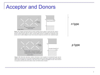
- 1. Acceptor and Donors 1 p type n type
- 2. 2 The principal characteristic of a pn-junction diode is that it allows current to flow easily in one direction but hardly at all in the other direction. We call these situations forward bias and reverse bias, respectively. pn-junction Diodes Here p-type and n-type semiconductors are joined together.
- 3. 3
- 4. 4
- 5. 5 Operation of a pn-junction Diode https://www.youtube.com/watch?v=cdTpvYozx5g
- 6. 6
- 7. 7 The diode is an important tool in many kinds of electrical circuits. As an example, consider the bridge rectifier circuit shown in Figure 11.14. The bridge rectifier is set up so that it allows current to flow in only one direction through the resistor R when an alternating current supply is placed across the bridge. The current through the resistor is then a rectified sine wave of the form This is the first step in changing alternating current to direct current. The design of a power supply can be completed by adding capacitors and resistors in appropriate proportions. This is an important application, because direct current is needed in many devices and the current that we get from our wall sockets is alternating current. Figure 11.14: Circuit diagram for a diode bridge rectifier. Bridge Rectifiers (11.10)
- 8. 8 The Zener diode is made to operate under reverse bias once a sufficiently high voltage has been reached. The I-V curve of a Zener diode is shown in Figure 11.15. Notice that under reverse bias and low voltage the current assumes a low negative value, just as in a normal pn-junction diode. But when a sufficiently large reverse bias voltage is reached, the current increases at a very high rate. Zener Diodes Figure 11.15: A typical I-V curve for a Zener diode. Figure 11.16: A Zener diode reference circuit.
- 9. 9 Light Emitting Diodes Another important kind of diode is the light-emitting diode (LED). Whenever an electron makes a transition from the conduction band to the valence band (effectively recombining the electron and hole) there is a release of energy in the form of a photon (Figure 11.17). In some materials the energy levels are spaced so that the photon is in the visible part of the spectrum. In that case, the continuous flow of current through the LED results in a continuous stream of nearly monochromatic light. Figure 11.17: Schematic of an LED. A photon is released as an electron falls from the conduction band to the valence band. The band gap may be large enough that the photon will be in the visible portion of the spectrum.
- 10. 10 Photovoltaic Cells An exciting application closely related to the LED is the solar cell, also known as the photovoltaic cell. Simply put, a solar cell takes incoming light energy and turns it into electrical energy. A good way to think of the solar cell is to consider the LED in reverse (Figure 11.18). A pn- junction diode can absorb a photon of solar radiation by having an electron make a transition from the valence band to the conduction band. In doing so, both a conducting electron and a hole have been created. If a circuit is connected to the pn junction, the holes and electrons will move so as to create an electric current, with positive current flowing from the p side to the n side. Even though the efficiency of most solar cells is low, their widespread use could potentially generate significant amounts of electricity. Remember that the “solar constant” (the energy per unit area of solar radiation reaching the Earth) is over 1400 W/m2, and more than half of this makes it through the atmosphere to the Earth’s surface. There has been tremendous progress in recent years toward making solar cells more efficient. Figure 11.18: (a) Schematic of a photovoltaic cell. Note the similarity to Figure 11.17. (b) A schematic showing more of the working parts of a real photovoltaic cell. From H. M. Hubbard, Science 244, 297-303 (21 April 1989).
- 12. 12
- 13. 13
- 14. 14
- 15. 15 Consider now the npn junction in the circuit shown in Figure 11.23a. If the emitter is more heavily doped than the base, then there is a heavy flow of electrons from left to right into the base. The base is made thin enough so that virtually all of those electrons can pass through the collector and into the output portion of the circuit. As a result the output current is a very high fraction of the input current. The key now is to look at the input and output voltages. Because the base-collector combination is essentially a diode connected in reverse bias, the voltage on the output side can be made higher than the voltage on the input side. Recall that the output and input currents are comparable, so the resulting output power (current × voltage) is much higher than the input power. Transistors Figure 11.23: (a) The npn transistor in a voltage amplifier circuit. (b) The circuit has been modified to put the input between base and ground, thus making a current amplifier. (c) The same circuit as in (b) using the transistor circuit symbol.
- 16. 16 Field Effect Transistors (FET) The three terminals of the FET are known as the drain, source, and gate, and these correspond to the collector, emitter, and base, respectively, of a bipolar transistor. Figure 11.25: (a) A schematic of a FET. The two gate regions are connected internally. (b) The circuit symbol for the FET, assuming the source-to-drain channel is of n-type material and the gate is p-type. If the channel is p-type and the gate n-type, then the arrow is reversed. (c) An amplifier circuit containing a FET.
- 17. 17
- 18. 18 Schottky Barriers Here a direct contact is made between a metal and a semiconductor. If the semiconductor is n-type, electrons from it tend to migrate into the metal, leaving a depleted region within the semiconductor. This will happen as long as the work function of the metal is higher (or lower, in the case of a p-type semiconductor) than that of the semiconductor. The width of the depleted region depends on the properties of the particular metal and semiconductor being used, but it is typically on the order of microns. The I-V characteristics of the Schottky barrier are similar to those of the pn-junction diode. When a p-type semiconductor is used, the behavior is similar but the depletion region has a deficit of holes.
- 19. 19 Schottky Barriers Figure 11.26: (a) Schematic drawing of a typical Schottky-barrier FET. (b) Gain versus frequency for two different substrate materials, Si and GaAs. From D. A. Fraser, Physics of Semiconductor Devices, Oxford: Clarendon Press (1979).
- 20. 20 Semiconductor Lasers Like the gas lasers described in Section 10.2, semiconductor lasers operate using population inversion—an artificially high number of electrons in excited states In a semiconductor laser, the band gap determines the energy difference between the excited state and the ground state Semiconductor lasers use injection pumping, where a large forward current is passed through a diode creating electron-hole pairs, with electrons in the conduction band and holes in the valence band. A photon is emitted when an electron falls back to the valence band to recombine with the hole.
- 21. 21 Semiconductor Lasers Since their development, semiconductor lasers have been used in a number of applications, most notably in fiber-optics communication. One advantage of using semiconductor lasers in this application is their small size with dimensions typically on the order of 10−4 m. Being solid-state devices, they are more robust than gas-filled tubes.
- 22. 22 Integrated Circuits The most important use of all these semiconductor devices today is not in discrete components, but rather in integrated circuits called chips. Some integrated circuits contain a million or more components such as resistors, capacitors, and transistors. Two benefits: miniaturization and processing speed.
- 23. 23
- 24. 24 11.4: Nanotechnology Nanotechnology is generally defined as the scientific study and manufacture of materials on a submicron scale. These scales range from single atoms (on the order of .1 nm up to 1 micron (1000 nm). This technology has applications in engineering, chemistry, and the life sciences and, as such, is interdisciplinary.
- 25. 25 Carbon Nanotubes In 1991, following the discovery of C60 buckminsterfullerenes, or “buckyballs,” Japanese physicist Sumio Iijima discovered a new geometric arrangement of pure carbon into large molecules. In this arrangement, known as a carbon nanotube, hexagonal arrays of carbon atoms lie along a cylindrical tube instead of a spherical ball.
- 26. 26 Structure of a Carbon Nanotube Figure 11.30: Model of a carbon nanotube, illustrating the hexagonal carbon pattern superimposed on a tubelike structure. There is virtually no limit to the length of the tube. From http://www.hpc.susx.ac.uk/ ~ewels/img/science/nanotubes/.
- 27. 27 Carbon Nanotubes The basic structure shown in Figure 11.30 leads to two types of nanotubes. A single-walled nanotube has just the single shell of hexagons as shown. In a multi-walled nanotube, multiple layers are nested like the rings in a tree trunk. Single-walled nanotubes tend to have fewer defects, and they are therefore stronger structurally but they are also more expensive and difficult to make.
- 28. 28 Applications of Nanotubes By their strength they are used as structural reinforcements in the manufacture of composite materials (batteries in cell-phones use nanotubes in this way) Nanotubes have very high electrical and thermal conductivities, and as such lead to high current densities in high-temperature superconductors.
- 29. 29 Nanoscale Electronics One problem in the development of truly small-scale electronic devices is that the connecting wires in any circuit need to be as small as possible, so that they do not overwhelm the nanoscale components they connect. In addition to the nanotubes already described, semiconductor wires (for example indium phosphide) have been fabricated with diameters as small as 5 nm.
- 30. 30 Nanoscale Electronics These nanowires have been shown useful in connecting nanoscale transistors and memory circuits. These are referred to as nanotransistors.
- 31. 31 Nanotechnology and the Life Sciences The complex molecules needed for the variety of life on Earth are themselves examples of nanoscale design. Examples of unusual materials designed for specific purposes include the molecules that make up claws, feathers, and even tooth enamel.
- 32. 32 Information Science It’s possible that current photolithographic techniques for making computer chips could be extended into the hard-UV or soft x-ray range, with wavelengths on the order of 1 nm, to fabricate silicon-based chips on that scale. Possible quantum effects as devices become smaller, specifically the superposition of quantum states possibly leading to quantum computing.
- 33. 33