08448380779 Call Girls In Friends Colony Women Seeking Men
DRV401AIDWPG4
1. DRV401
SBVS070B − JUNE 2006 − REVISED MAY 2009
Sensor Signal Conditioning IC for
Closed-Loop Magnetic Current Sensor
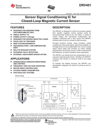
FEATURES DESCRIPTION
D DESIGNED FOR SENSORS FROM The DRV401 is designed to control and process signals
VACUUMSCHMELZE (VAC) from specific magnetic current sensors made by
D SINGLE SUPPLY: 5V Vacuumschmelze GmbH & Co. KG (VAC). A variety of
D POWER OUTPUT: H-Bridge current ranges and mechanical configurations are
D DESIGNED FOR DRIVING INDUCTIVE LOADS available. Combined with a VAC sensor, the DRV401
monitors both ac and dc currents to high accuracy.
D EXCELLENT DC PRECISION
D WIDE SYSTEM BANDWIDTH Provided functions include: probe excitation, signal
conditioning of the probe signal, signal loop amplifier, an
D HIGH-RESOLUTION, LOW-TEMPERATURE
H-bridge driver for the compensation coil, and an analog
DRIFT
signal output stage that provides an output voltage
D BUILT-IN DEGAUSS SYSTEM proportional to the primary current. It offers overload and
D EXTENSIVE FAULT DETECTION fault detection, as well as transient noise suppression.
D EXTERNAL HIGH-POWER DRIVER OPTION The DRV401 can directly drive the compensation coil, or
connect to external power drivers. Therefore, the DRV401
APPLICATIONS combines with sensors to measure small to very large
currents.
D GENERATOR/ALTERNATOR MONITORING
AND CONTROL To maintain the highest accuracy, the DRV401 can
D FREQUENCY AND VOLTAGE INVERTERS demagnetize (degauss) the sensor at power-up and on
demand.
D MOTOR DRIVE CONTROLLERS
D SYSTEM POWER CONSUMPTION
D PHOTOVOLTAIC SYSTEMS
Patents Pending.
Compensation
RS
PWM PWM ICOMP1 ICOMP2
Compensation Winding
Primary Winding DRV401
Diff
Magnetic Core
Amp
Field Probe
IS2
IP VOUT
IS1 REFIN
Probe Integrator H−Bridge
Interface Filter Driver
Timing, Error Detection, VREF
Degauss VREF
and Power Control
+5V GND
Please be aware that an important notice concerning availability, standard warranty, and use in critical applications of Texas Instruments
semiconductor products and disclaimers thereto appears at the end of this data sheet.
PowerPAD is a trademark of Texas Instruments. All other trademarks are the property of their respective owners.
PRODUCTION DATA information is current as of publication date. Products Copyright 2006−2009, Texas Instruments Incorporated
conform to specifications per the terms of Texas Instruments standard warranty.
Production processing does not necessarily include testing of all parameters.
www.ti.com
2. DRV401
www.ti.com
SBVS070B − JUNE 2006 − REVISED MAY 2009
This integrated circuit can be damaged by ESD. Texas
ABSOLUTE MAXIMUM RATINGS(1) Instruments recommends that all integrated circuits be
Supply Voltage . . . . . . . . . . . . . . . . . . . . . . . . . . . . . . . . . . . . . . . +7V handled with appropriate precautions. Failure to observe
Signal Input Terminals: proper handling and installation procedures can cause damage.
Voltage(2) . . . . . . . . . . . . . . . . . . . . . . . . . . . −0.5V to VDD + 0.5V
ESD damage can range from subtle performance degradation to
Differential Amplifier(3) . . . . . . . . . . . . . . . . . . . . . . −10V to +10V complete device failure. Precision integrated circuits may be more
Current at IS1 and IS2 . . . . . . . . . . . . . . . . . . . . . . . . . . . . . ±75mA susceptible to damage because very small parametric changes could
Current (pins other than IS1 and IS2)(2) . . . . . . . . . . . . . . ±25mA cause the device not to meet its published specifications.
ICOMP Short Circuit(4) . . . . . . . . . . . . . . . . . . . . . . . . . . . . . +250mA
Operating Junction Temperature . . . . . . . . . . . . . −50°C to +150°C ORDERING INFORMATION(1)
Storage Temperature . . . . . . . . . . . . . . . . . . . . . . . −55°C to +150°C
PACKAGE PACKAGE
ESD Rating: PRODUCT PACKAGE-LEAD
DESIGNATOR MARKING
Human Body Model (HBM)
QFN-20
Pins IAIN1 and IAIN2 Only . . . . . . . . . . . . . . . . . . . . . . . . . . . 1kV DRV401 RGW HAAQ
(5mm x 5mm)
All Other Pins . . . . . . . . . . . . . . . . . . . . . . . . . . . . . . . . . . . . . 4kV
DRV401 SO-20 DWP DRV401A
(1) Stresses above these ratings may cause permanent damage.
(1) For the most current package and ordering information see the
Exposure to absolute maximum conditions for extended periods
may degrade device reliability. These are stress ratings only, and Package Option Addendum at the end of this document, or see
functional operation of the device at these or any other conditions the TI web site at www.ti.com.
beyond those specified is not supported.
(2) Input terminals are diode-clamped to the power-supply rails.
Input signals that can swing more than 0.5V beyond the supply
rails must be current limited, except for the differential amplifier
input pins.
(3) These inputs are not internally protected against over voltage.
The differential amplifier input pins must be limited to 5mA, max or
±10V, max.
(4) Power-limited; observe maximum junction temperature.
2
3. DRV401
www.ti.com
SBVS070B − JUNE 2006 − REVISED MAY 2009
ELECTRICAL CHARACTERISTICS
Boldface limits apply over the specified temperature range: TJ = −40°C to +125°C.
At TA = +25°C and VDD1 = VDD2 = +5V with external 100kHz filter BW, and zero output current ICOMP, unless otherwise noted.
DRV401
PARAMETER CONDITIONS MIN TYP MAX UNITS
DIFFERENTIAL AMPLIFIER RL = 10kΩ to 2.5V, VREFIN = 2.5V
OFFSET VOLTAGE
Offset Voltage, RTO(1)(2) VOS Gain 4V/V ±0.01 ±0.1 mV
Drift, RTO(2) dVOS/dT ±0.1 ±1(3) µV/°C
vs Common-Mode, RTO CMRR −1V to +6V, VREF = 2.5V ±50 ±250 µV/V
vs Power-Supply, RTO PSRR VREF not included ±4 ±50 µV/V
SIGNAL INPUT
Common-Mode Voltage Range −1 (VDD) + 1 V
SIGNAL OUTPUT
Signal Over-Range Indication (OVER-RANGE), Delay(2) VIN = 1V Step, See Notes 2 and 3 2.5 to 3.5 µs
Voltage Output Swing From Negative Rail(2),
I = +2.5mA, CMP Trip Level +48 +85 mV
OVER-RANGE Trip Level
Voltage Output Swing From Positive Rail(2),
I = −2.5mA, CMP Trip Level VDD − 85 VDD − 48 mV
OVER-RANGE Trip Level
Short-Circuit Current(2) ISC VOUT Connected To GND −18 mA
VOUT Connected To VDD +20 mA
Gain, VOUT/VIN_DIFF 4 V/V
Gain Error ±0.02 ±0.3 %
Gain Error Drift ±0.1 ppm/°C
Linearity Error RL = 1kΩ 10 ppm
FREQUENCY RESPONSE
Bandwidth(2) BW−3dB 2 MHz
Slew Rate(2) SR CMVR = −1V to = +4V 6.5 V/µs
Settling Time, Large-Signal(2) dV ± 2V to 1%, No External Filter 0.9 µs
Settling Time(2) dV ± 0.4V to 0.01% 14 µs
INPUT RESISTANCE
Differential 16.5 20 23.5 kΩ
Common-Mode 41 50 59 kΩ
External Reference Input 41 50 59 kΩ
NOISE
Output Voltage Noise Density, f = 1kHz, RTO(2) en Compensation Loop Disabled 170 nV/√Hz
COMPENSATION LOOP
DC STABILITY Probe f = 250kHz, RLOAD = 20Ω
Offset Error(4) Deviation from 50% PWM, Pin Gain = L 0.03 %
Offset Error Drift(2) Deviation from 50% PWM, Pin Gain = L 7.5 ppm/°C
Gain, Pin Gain = L(2) |VICOMP1| − |VICOMP2| −200 25 200 ppm/V
Power-Supply Rejection Ratio PSRR Probe Loop f = 250kHz 500 ppm/V
FREQUENCY RESPONSE
Open-Loop Gain, Two Modes, 7.8kHz Pin Gain H/L 24/32 dB
PROBE COIL LOOP
Input Voltage Clamp Range Field Probe Current < 50mA −0.7 to VDD + 0.7 V
Internal Resistor, IS1 or IS2 to VDD1(2) RHIGH 47 59 71 Ω
Internal Resistor, IS1 or IS2 to GND1(2) RLOW 60 75 90 Ω
Resistance Mismatch Between IS1 and IS2(2) ppm of RHIGH + RLOW 300 1500 ppm
Total Input Resistance(3) 134 200 W
Comparator Threshold Current(3) 22 28 34 mA
Minimum Probe Loop Half-Cycle(2) 250 280 310 ns
Probe Loop Minimum Frequency 250 kHz
No Oscillation Detect (Error) Suppression 35 µs
COMPENSATION COIL DRIVER, H-BRIDGE
Peak Current(2) VICOMP1 − VICOMP2 = 4.0VPP 250 mA
Voltage Swing 20Ω Load 4.2 VPP
Output Common-Mode Voltage VDD2/2 V
Wire Break Detect, Threshold Current(5) ICOMP1 and ICOMP2 Railed 33 57 mA
3
4. DRV401
www.ti.com
SBVS070B − JUNE 2006 − REVISED MAY 2009
ELECTRICAL CHARACTERISTICS (continued)
Boldface limits apply over the specified temperature range, TJ = −40°C to +125°C, with zero output current ICOMP.
At TA = +25°C and VDD1 = VDD2 = +5V with external 100kHz filter BW, unless otherwise noted.
DRV401
PARAMETER CONDITIONS MIN TYP MAX UNITS
VOLTAGE REFERENCE
Voltage(2) No Load 2.495 2.5 2.505 V
Drift(2) No Load ±5 ±50 ppm/°C
PSRR(2) ±15 ±200 µV/V
Load Regulation(2) Load to GND/VDD, dI = 0mA to 5mA 0.15 mV/mA
Short-Circuit Current ISC REFOUT Connected to VDD +20 mA
REFOUT Connected to GND −18 mA
DEMAGNETIZATION
Duration See Timing Diagram 106 130(3) ms
DIGITAL I/O
LOGIC INPUTS (DEMAG, GAIN, and CCdiag Pins) CMOS Type Levels
Pull-Up High Current (CCdiag) 3.5 < VIN < VDD 160 µA
Pull-Up Low Current (CCdiag) 0 < VIN < 1.5 5 µA
Logic Input Leakage Current 0 < VIN < VDD 0.01 5 µA
Logic Level, Input: L/H 2.1/2.8 V
Hysteresis 0.7 V
OUTPUTS (ERROR AND OVER-RANGE Pins)
Logic Level, Output: L 4mA Sink 0.3 V
Logic Level, Output: H No Internal Pull-Up
OUTPUTS (PWM and PWM Pins) Push-Pull Type
Logic Level L 4mA Sink 0.2 V
Logic Level H 4mA Source (VDD) − 0.4 V
POWER SUPPLY
Specified Voltage Range VDD 4.5 5 5.5 V
Power-On Reset Threshold VRST 1.8 V
Quiescent Current [I(VDD1) + I(VDD2)] IQ ICOMP = 0mA, Sensor Not Connected 6.8 mA
Brownout Voltage Level(2) 4 V
Brownout Indication Delay 135 µs
TEMPERATURE RANGE
Specified Range TJ −40 +125 °C
Operating Range TJ −50 +150 °C
Package Thermal Resistance
QFN Surface-Mount qJA See Note 6 40 °C/W
SO PowerPAD Surface-Mount qJA See Note 6 27 °C/W
(1) Parameter value referred to output (RTO).
(2) See Typical Characteristic curves.
(3) Total input resistance and comparator threshold current are inversely related. See Figure 2a.
(4) For VAC sensors, 0.2% of PWM offset approximately corresponds to 10mA primary current offset per winding.
(5) See Compensation Driver section in Applications Information.
(6) See Applications Information section for information on power dissipation, layout considerations, and proper PCB soldering and heat-sinking technique.
4
5. DRV401
www.ti.com
SBVS070B − JUNE 2006 − REVISED MAY 2009
PIN CONFIGURATIONS
Top View RGW Top View DWP
GND1
PWM
PWM
PWM 1 20 IS1
IS1
IS2
PWM 2 19 GND1
20
19
18
17
16
ERROR 3 18 IS2
ERROR 1 15 VDD1
DEMAG 4 17 VDD1
DEMAG 2 Exposed 14 OVER−RANGE Exposed
Thermal Pad GAIN 5 Thermal Pad 16 OVER−RANGE
GAIN 3 on Underside, 13 CCdiag on Underside,
Connect REFOUT 6 Connect 15 CCdiag
REFOUT 4 to GND1 12 VDD2
to GND1
REFIN 7 14 VDD2
REFIN 5 11 ICOMP1
VOUT 8 13 ICOMP1
10
6
7
8
9
IAIN2 9 12 ICOMP2
VOUT
IAIN2
IAIN1
ICOMP2
GND2
IAIN1 10 11 GND2
QFN−20 (5mm x 5mm) Wide−Body SO−20
PIN ASSIGNMENTS
NAME RGW DWP DESCRIPTION
ERROR 1 3 Error flag: open-drain output, see the Error Conditions section.
DEMAG 2 4 Control input, see the Demagnetization section.
GAIN 3 5 Control input for open-loop gain: low = normal, high = −8dB.
REFOUT 4 6 Output for internal 2.5V reference voltage.
REFIN 5 7 Input for zero reference to differential amplifier.
VOUT 6 8 Output for differential amplifier.
IAIN2 7 9 Noninverting input of differential amplifier.
IAIN1 8 10 Inverting input of differential amplifier.
GND2 9 11 Ground connection. Connect to GND1.
ICOMP2 10 12 Output 2 of compensation coil driver.
ICOMP1 11 13 Output 1 of compensation coil driver.
VDD2 12 14 Supply voltage. Connect to VDD1.
CCdiag 13 15 Control input for wire-break detection: high = enable.
OVER−RANGE 14 16 Open-drain output for over-range indication: low = over-range.
VDD1 15 17 Supply voltage.
IS2 16 18 Probe connection 2.
GND1 17 19 Ground connection.
IS1 18 20 Probe connection 1.
PWM 19 1 PWM output from probe circuit (inverted).
PWM 20 2 PWM output from probe circuit.
Exposed Thermal Pad — — Connect to GND1.
5
6. DRV401
www.ti.com
SBVS070B − JUNE 2006 − REVISED MAY 2009
TYPICAL CHARACTERISTICS
At TA = +25°C and VDD1 = VDD2 = +5V with external 100kHz filter BW, unless otherwise noted.
DRV401 AND SENSOR:
DRV401 AND SENSOR: OUTPUT VOLTAGE NOISE DENSITY
OFFSET vs SUPPLY VOLTAGE (Sensor M4645−X080, RSHUNT = 10Ω, Mode = Low)
0.04 100
0.03 60Hz Line Frequency and Multiples
(measured in a 60Hz environment)
0.02
M4645−X211
M4645−X211
VN (µV/√Hz)
0.01 Divided Field
IPRIM (A)
Probe Frequency
0 10
M4645−X080
−0.01
−0.02
−0.03
−0.04 0.1
4.1 4.3 4.5 4.7 4.9 5.1 5.3 5.5 5.7 5.9 6.1 0.1 1 10 100 1k 10k 100k
VDD (V) Frequency (Hz)
DRV401 AND SENSOR: ABSOLUTE ERROR
(Soldered DWP−20 with 1 Square−Inch Copper Pad) GAIN FLATNESS vs FREQUENCY
(Measurements by Vacuumschmelza GmbH) (Measurements by Vacuumschmelze GmbH)
0.3 1.20
T = −50_ C DRV401 with M4645−X600 Sensor
T = +25_C 1.15 DRV401 with M4645−X211 Sensor
0.2
T = +85_C DRV401 with M4645−X080 Sensor
T = +125_ C 1.10
Absolute Error (A)
Normalized Gain
0.1
1.05
0 1.00
0.95
−0.1
0.90
−0.2
0.85
TC (RSHUNT) ±25ppm/_ C.
−0.3 0.80
−300 −200 −100 0 100 200 300 10 100 1k 10k 100k 1M
Primary Current (A) Frequency (Hz)
DIFFERENTIAL AMPLIFIER:
3A ICOMP OVERLOAD RECOVERY VOLTAGE OFFSET PRODUCTION DISTRIBUTION
(Measurements by Vacuumschmelze GmbH)
RTO
Over−Range
Over−Range
Population
VOUT
2000A/div
2V/div
VOUT
ERROR
ERROR
IPRIM
IPRIM
NOTE: IPRIM = 3000A corresponds to ICOMP = 3A.
−50
−45
−40
−35
−30
−25
−20
−15
−10
−5
0
5
10
15
20
25
30
35
40
45
50
0 20 40 60 80 100 120 140 160 180 200
Time (µs) Voltage Offset (µV)
6
7. DRV401
www.ti.com
SBVS070B − JUNE 2006 − REVISED MAY 2009
TYPICAL CHARACTERISTICS (Continued)
At TA = +25°C and VDD1 = VDD2 = +5V with external 100kHz filter BW, unless otherwise noted.
DIFFERENTIAL AMPLIFIER: DIFFERENTIAL AMPLIFIER:
OFFSET VOLTAGE vs TEMPERATURE, RTO GAIN vs FREQUENCY
20 20
16 15
12
10
8
Input VOS (µV)
5
Gain (dB)
4
Sample Average
0 0
−4 −5
−8
−10
−12
−16 −15
−20 −20
−50 −25 0 25 50 75 100 125 150 10 100 1k 10k 100k 1M 10M
Temperature (_C) Frequency (Hz)
DIFFERENTIAL AMPLIFIER: DIFFERENTIAL AMPLIFIER:
PSRR AND CMRR vs FREQUENCY OUTPUT VOLTAGE vs OUTPUT CURRENT
120 5.0
PSRR −40_ C +25_C
100 4.9
+125_ C
PSRR and CMRR (dB)
4.8
Output Voltage (V)
CMRR
80
+85_ C
4.7
60
0.3
+125_C +85_C
40
0.2
20 0.1
+25_ C −40_C
0 0
10 100 1k 10k 100k 1M 2M 0 1 2 3 4 5 6 7 8 9 10
Frequency (Hz) Load Current (mA)
DIFFERENTIAL AMPLIFIER: DIFFERENTIAL AMPLIFIER:
OUTPUT NOISE DENSITY SHORT−CIRCUIT CURRENT vs TEMPERATURE
1000 25
VOUT Shorted to 5V
20
Short−Circuit Current (mA)
15
Noise Density (nV/√Hz)
10
5
100 0
−5
−10
Autozero Frequency = 69kHz −15
Sensor Not Running −20
en = 162nV/√Hz (average over 250Hz to 50kHz) VOUT Shorted to 0V
10 −25
100 1k 10k 100k 1M −50 −25 0 25 50 75 100 125 150
Frequency (Hz) Temperature (_ C)
7
8. DRV401
www.ti.com
SBVS070B − JUNE 2006 − REVISED MAY 2009
TYPICAL CHARACTERISTICS (Continued)
At TA = +25°C and VDD1 = VDD2 = +5V with external 100kHz filter BW, unless otherwise noted.
DIFFERENTIAL AMPLIFIER: DIFFERENTIAL AMPLIFIER:
TA = −50_C LARGE−SIGNAL STEP RESPONSE TA = +25_C LARGE−SIGNAL STEP RESPONSE
3.8 3.8
3.6 3.6
3.4 3.4
3.2 3.2
3.0 3.0
Voltage (V)
Voltage (V)
2.8 2.8
2.6 2.6
2.4 2.4
2.2 2.2
2.0 2.0
1.8 1.8
1.6 1.6
1.4 1.4
1µs/div 1µs/div
DIFFERENTIAL AMPLIFIER: DIFFERENTIAL AMPLIFIER:
TA = +150_C LARGE−SIGNAL STEP RESPONSE OVER−RANGE DELAY vs TEMPERATURE
3.8 3.5
At 5.0V
3.6 3.4 VIN Step 0V to ±1V
3.4
3.3
Over−Range Delay (µs)
3.2
3.0 3.2
Negative Over−Range
Voltage (V)
2.8 3.1
2.6 3.0
2.4 2.9
2.2 Positive Over−Range
2.8
2.0
2.7
1.8
1.6 2.6
1.4 2.5
1µs/div −50 −25 0 25 50 75 100 125 150
Temperature (_ C)
DIFFERENTIAL AMPLIFIER: DIFFERENTIAL AMPLIFIER:
POSITIVE SLEW RATE vs TEMPERATURE NEGATIVE SLEW RATE vs TEMPERATURE
7.5 −6.5
At 5.0V At 5.0V
7.4 −6.6
7.3 −6.7
7.2 −6.8
Slew Rate (V/µs)
Slew Rate (V/µs)
7.1 −6.9
7.0 −7.0
6.9 −7.1
6.8 −7.2
6.7 −7.3
6.6 −7.4
6.5 −7.5
−50 −25 0 25 50 75 100 125 150 −50 −25 0 25 50 75 100 125 150
Temperature (_ C) Temperature (_ C)
8
9. DRV401
www.ti.com
SBVS070B − JUNE 2006 − REVISED MAY 2009
TYPICAL CHARACTERISTICS (Continued)
At TA = +25°C and VDD1 = VDD2 = +5V with external 100kHz filter BW, unless otherwise noted.
DIFFERENTIAL AMPLIFIER: COMPENSATION LOOP:
REFIN RESISTANCE vs TEMPERATURE SMALL−SIGNAL GAIN
Gain VPWMAVERAGE /(VICOMP1, VICOMP2) (dB)
50.250 70
60
50.125
50
RREF IN (kΩ )
Pin Gain = Low
50.000
40
Pin Gain = High
49.875 30
20
49.750
10
49.625 0
−50 −25 0 25 50 75 100 125 150 100 1k 10k 100k
Temperature (_ C) Frequency (Hz)
COMPENSATION LOOP: COMPENSATION LOOP:
DUTY CYCLE ERROR vs TEMPERATURE DC GAIN: DUTY CYCLE ERROR CHANGE
2000
VICOMP1 − VICOMP2 = 4.2V
1500 ILOAD = 210mA
Gain Pin Low
Duty Cycle Error (ppm)
1000
500
Population
0
At 250kHz, 5.0V
−500
−1000
At 400kHz, 5.0V
−1500
−2000
−50 −25
−200
−180
−160
−140
−120
−100
−80
−60
−40
−20
0 25 50 75 100 125 150
0
20
40
60
80
100
120
140
160
180
200
Temperature (_ C)
Gain (ppm/V)
ICOMP OUTPUT SWING TO RAIL PROBE COMPARATOR THRESHOLD
vs OUTPUT CURRENT CURRENT vs TEMPERATURE
Probe Comparator Threshold Current (mA)
5.00 35.0
4.75
+125_C +25_ C −50_ C
4.50
32.5
Output Swing (V)
4.25
4.00
30.0
1.00
0.75
0.50 27.5
+125_C +25_ C −50_ C
0.25
0 25.0
0 50 100 150 200 250 300 −50 −25 0 25 50 75 100 125 150
Output Current (mA) Temperature (_ C)
9
10. DRV401
www.ti.com
SBVS070B − JUNE 2006 − REVISED MAY 2009
TYPICAL CHARACTERISTICS (Continued)
At TA = +25°C and VDD1 = VDD2 = +5V with external 100kHz filter BW, unless otherwise noted.
PROBE DRIVER: OUTPUT IMPEDANCE MISMATCH OF IS1 AND IS2
INTERNAL RESISTOR vs TEMPERATURE vs TEMPERATURE
90 0.10
Output Impedance Mismatch (Ω )
85
80 0.08
Driver L
75
Resistance (Ω)
0.06
70
65
0.04
60
Driver H
55 0.02
50
45 0
−50 −25 0 25 50 75 100 125 150 −50 −25 0 25 50 75 100 125 150
Temperature (_ C) Temperature (_ C)
VOLTAGE REFERENCE vs LOAD CURRENT VOLTAGE REFERENCE PRODUCTION DISTRIBUTION
2.5010
2.5008
2.5006
2.5004
Population
2.5002
VREF (V)
2.5000
2.4998
2.4996
2.4994
2.4992
2.4990
−6 −4 −2 0 2 4 6
2.4950
2.4955
2.4960
2.4965
2.4970
2.4975
2.4980
2.4985
2.4990
2.4995
2.5000
2.5005
2.5010
2.5015
2.5020
2.5025
2.5030
2.5035
2.5040
2.5045
2.5050
ILOAD (mA)
VREF (V)
VOLTAGE REFERENCE DRIFT
PRODUCTION DISTRIBUTION
VOLTAGE REFERENCE vs TEMPERATURE
2.525
2.520
2.515
2.510
Population
2.505
VREF (V)
2.500
2.495
2.490
2.485
2.480
0
2.5
5.0
7.5
10.0
12.5
15.0
17.5
20.0
22.5
25.0
27.5
30.0
32.5
35.0
37.5
40.0
42.5
45.0
47.5
50.0
2.475
−50 −25 0 25 50 75 100 125 150
Voltage Reference Drift (ppm/_ C) Temperature (_ C)
10
11. DRV401
www.ti.com
SBVS070B − JUNE 2006 − REVISED MAY 2009
TYPICAL CHARACTERISTICS (Continued)
At TA = +25°C and VDD1 = VDD2 = +5V with external 100kHz filter BW, unless otherwise noted.
VOLTAGE REFERENCE POWER−SUPPLY REJECTION
PRODUCTION DISTRIBUTION OSCILLATOR PRODUCTION DISTRIBUTION
Population
Population
250
253
256
259
262
265
268
271
274
277
280
283
286
289
292
295
298
301
304
307
310
−200
−175
−150
−125
−100
−75
−50
−25
0
25
50
75
100
125
150
175
200
PSR (µV/V) Minimum Probe Loop Half−Cycle (ns)
OSCILLATOR vs TEMPERATURE OSCILLATOR vs SUPPLY VOLTAGE
310 310
Minimum Probe Loop Half−Cycle (ns)
Minimum Probe Loop Half−Cycle (ns)
305 305
300 300
295 295
290 290
285 285
280 280
275 275
270 270
265 265
260 260
255 255
250 250
−50 −25 0 25 50 75 100 125 150 4.3 4.6 4.9 5.2 5.5 5.8 6.0
Temperature (_C) VDD (V)
BROWN−OUT VOLTAGE vs TEMPERATURE
4.20
4.15
Brown−Out Voltage (V)
4.10
4.05
4.00
3.95
3.90
3.85
3.80
−50 −25 0 25 50 75 100 125 150
Temperature (_ C)
11