SlideShare une entreprise Scribd logo
1  sur  16
2
Text Books:
• Neil H.Weste, Harris, A. Banerjee, CMOS VLSI Design, A circuits and System Perspective, 2015, 4th
Edition, Pearson Education, Noida, India.
• http://emicroelectronics.free.fr/onlineCourses/VLSI/toc.html
(Design of VLSI Systems, Yusuf Leblebici)
Reference Books:
• Sung-Mo Kang, Yusuf Liblebici, Chulwoo Kim, CMOS Digital Integrated Circuits: Analysis and
Design, 2019, Revised 4th Edition, Tata Mc Graw Hill, New Delhi, India.
IntegratedCircuit-Moore’sLaw
• Moore's law (In year 1975) is the observation that the number of transistors in an integrated
circuit (IC) doubles about every two years.
• Moore's law is an observation/empirical relationship and projection of a historical trend,
rather than a law of physics.
• The observation is named after Gordon Moore, the co-founder of Fairchild Semiconductor
and former CEO of the Intel (Integrated Electronics).
• The level of integration as measured by the number of logic gates in a monolithic chip has
been steadily rising for almost three decades.
Evolution of logic complexity in integrated circuits
• Less area/volume and therefore, compactness
• Less power consumption
• Less testing requirements at system level
• Higher reliability, mainly due to improved on-chip interconnects
• Higher speed, due to significantly reduced interconnection length
• Significant cost savings
IntegratedCircuit–DesignObjectives/Performancemetrics
VLSIDesignFlow-DesignPartitioning
Flowchart of VLSI design flow
Front end design (Involves gate
level HDL-EDA tools)
Back end design (Involves
transistor level CAD tools)
Architectural Design: User’s
perspective, what does it do?
Example: Instruction set, registers
MIPS, x86, Alpha,
PIC, ARM, …
Functional Design
Example: Single cycle, multcycle,
pipelined, superscalar?
Logic: how are functional blocks
constructed
Example: Ripple carry, carry
lookahead, carry select adders
Circuit: how are transistors used
Example: Complementary
CMOS, pass transistors, domino
5
VLSIDesignFlow
• The design process, at various levels, is usually evolutionary in nature.
• It starts with a given set of requirements. Initial design is developed and tested
against the requirements.
• When requirements are not met, the design has to be improved.
• If such improvement is either not possible or too costly, then the revision of
requirements and its impact analysis must be considered.
• The Y-chart (first introduced by D.
Gajski) shown in Figure illustrates a
design flow for most logic chips, using
design activities on three different axes
(domains) which resemble the letter Y.
• The Y-chart consists of three major
domains, namely:
• behavioral domain
• structural domain
• geometrical layout/Physical domain
VLSIDesignFlow::Y-chart
• Although the design process has been described in linear fashion for simplicity, in reality
there are many iterations back and forth, especially between any two neighboring steps, and
occasionally even remotely separated pairs.
• Although top-down design flow provides an excellent design process control, in reality,
there is no truly unidirectional top-down design flow. Both top-down and bottom-up
approaches have to be combined.
VLSIDesignFlow
• The use of hierarchy, or “divide and
conquer” technique involves dividing a
module into sub- modules and then
repeating this operation on the sub-
modules until the complexity of the
smaller parts becomes manageable.
• This approach is very similar to the
software case where large programs are
split into smaller and smaller sections
until simple subroutines, with well-
defined functions and interfaces, can be
written.
• A hierarchy structure can be described
in each domain (shown in Y-chart)
separately.
VLSIDesignHierarchy
VLSIDesignHierarchy::Structuraldomainexample-
Decompositionofafour-bitaddercircuit
VLSIDesignHierarchy:: Conceptsof Regularity,ModularityandLocality
The VLSI design hierarchy mush take care/satisfy of the following concepts.
Regularity:
The hierarchical decomposition of a large system should result in not only simple, but also
similar blocks, as much as possible. Regularity usually reduces the number of different
modules that need to be designed and verified, at all levels of abstraction.
Modularity:
The various functional blocks which make up the larger system must have well-defined
functions and interfaces.
Locality:
Internal details remain at the local level. The concept of locality also ensures that
connections are mostly between neighboring modules, avoiding long-distance
connections as much as possible.
VLSIDesignStyles
• Standard IC
• Application specific IC (ASIC) : Following are the various ASIC Design Styles
VLSIDesignStyles::full-custom
In full-custom style, the designer has many degrees of freedom to optimize a circuit design:
• Adjust individual transistor dimensions (channel width, channel length, aspect ratio, etc.)
to satisfy:
• DC specifications (voltage levels, switching thresholds)
• Transient specifications (delay times, rise- and fall-times)
• Freely choose the most appropriate topology (placement and routing) for each circuit
block.
• Decide for the interconnection strategy between neighboring blocks.
• Decide for the global distribution of power, ground and clock.
VLSIDesignStyles::standardcell
Each standard cell is pre-designed,
with:
• Same cell height for all elements in
the library
• Horizontal PWR and GND lines at
the top and at the bottom
• Fixed pin locations (inputs and
outputs)
“Routing"
Between
the cells
VLSIDesignStyles::standardcell-Examples
Every standard cell
is pre-designed for
different channel
widths to facilitate
current drive
capability.
VLSIDesignStyles::FPGA
Field Programmable Gate Array (FPGA):
• Fully fabricated FPGA chips containing thousands of logic gates or even more, with
programmable interconnects, are available to users for their custom hardware programming
to realize desired functionality.
• This design style provides a means for fast prototyping and also for cost-effective chip
design, especially for low-volume applications.
• A typical field programmable gate array (FPGA) chip consists of I/O buffers, an array of
configurable logic blocks (CLBs), and programmable interconnect structures.
• The programming of the interconnects is implemented by programming of RAM cells
whose output terminals are connected to the gates of MOS pass transistors.
VLSIDesignStyles::FPGA-Example
General architecture of Xilinx FPGAs.

Contenu connexe

Similaire à Module 1 VLSID Design flow - Copy.pptx

unit 1vlsi notes.pdf
unit 1vlsi notes.pdfunit 1vlsi notes.pdf
unit 1vlsi notes.pdfAcademicICECE
 
ics123-03-architectural-styles.ppt
ics123-03-architectural-styles.pptics123-03-architectural-styles.ppt
ics123-03-architectural-styles.pptHamzakhalid708089
 
1 VLSI Introduction.pptx
1 VLSI Introduction.pptx1 VLSI Introduction.pptx
1 VLSI Introduction.pptxShishirAhmed39
 
SKEL 4273 CAD with HDL Topic 1
SKEL 4273 CAD with HDL Topic 1SKEL 4273 CAD with HDL Topic 1
SKEL 4273 CAD with HDL Topic 1alhadi81
 
Vlsi physical design-notes
Vlsi physical design-notesVlsi physical design-notes
Vlsi physical design-notesDr.YNM
 
Digital VLSI Design : Introduction
Digital VLSI Design : IntroductionDigital VLSI Design : Introduction
Digital VLSI Design : IntroductionUsha Mehta
 
Cross layer design and optimization
Cross layer design and optimizationCross layer design and optimization
Cross layer design and optimizationDANISHAMIN950
 
Software Architectures, Week 2 - Decomposition techniques
Software Architectures, Week 2 - Decomposition techniquesSoftware Architectures, Week 2 - Decomposition techniques
Software Architectures, Week 2 - Decomposition techniquesAngelos Kapsimanis
 
10 architectural design
10 architectural design10 architectural design
10 architectural designAyesha Bhatti
 
10 architectural design (1)
10 architectural design (1)10 architectural design (1)
10 architectural design (1)Ayesha Bhatti
 
Architectural design1
Architectural design1Architectural design1
Architectural design1Zahid Hussain
 
Architectural design1
Architectural design1Architectural design1
Architectural design1Zahid Hussain
 
VLSI UNIT-1.1.pdf.ppt
VLSI UNIT-1.1.pdf.pptVLSI UNIT-1.1.pdf.ppt
VLSI UNIT-1.1.pdf.pptrajukolluri
 

Similaire à Module 1 VLSID Design flow - Copy.pptx (20)

High bit rate_mul
High bit rate_mulHigh bit rate_mul
High bit rate_mul
 
unit 1vlsi notes.pdf
unit 1vlsi notes.pdfunit 1vlsi notes.pdf
unit 1vlsi notes.pdf
 
ics123-03-architectural-styles.ppt
ics123-03-architectural-styles.pptics123-03-architectural-styles.ppt
ics123-03-architectural-styles.ppt
 
1 VLSI Introduction.pptx
1 VLSI Introduction.pptx1 VLSI Introduction.pptx
1 VLSI Introduction.pptx
 
Floor planning ppt
Floor planning pptFloor planning ppt
Floor planning ppt
 
SKEL 4273 CAD with HDL Topic 1
SKEL 4273 CAD with HDL Topic 1SKEL 4273 CAD with HDL Topic 1
SKEL 4273 CAD with HDL Topic 1
 
Vlsi physical design-notes
Vlsi physical design-notesVlsi physical design-notes
Vlsi physical design-notes
 
VLSI design flow.pptx
VLSI design flow.pptxVLSI design flow.pptx
VLSI design flow.pptx
 
Digital VLSI Design : Introduction
Digital VLSI Design : IntroductionDigital VLSI Design : Introduction
Digital VLSI Design : Introduction
 
Report
ReportReport
Report
 
Hierarchical design and design abstraction
Hierarchical design and design abstractionHierarchical design and design abstraction
Hierarchical design and design abstraction
 
Cross layer design and optimization
Cross layer design and optimizationCross layer design and optimization
Cross layer design and optimization
 
Vlsi physical design (Back End Process)
Vlsi physical design (Back End Process)Vlsi physical design (Back End Process)
Vlsi physical design (Back End Process)
 
Software Architectures, Week 2 - Decomposition techniques
Software Architectures, Week 2 - Decomposition techniquesSoftware Architectures, Week 2 - Decomposition techniques
Software Architectures, Week 2 - Decomposition techniques
 
10 architectural design
10 architectural design10 architectural design
10 architectural design
 
10 architectural design (1)
10 architectural design (1)10 architectural design (1)
10 architectural design (1)
 
VLSI- Unit I
VLSI- Unit IVLSI- Unit I
VLSI- Unit I
 
Architectural design1
Architectural design1Architectural design1
Architectural design1
 
Architectural design1
Architectural design1Architectural design1
Architectural design1
 
VLSI UNIT-1.1.pdf.ppt
VLSI UNIT-1.1.pdf.pptVLSI UNIT-1.1.pdf.ppt
VLSI UNIT-1.1.pdf.ppt
 

Dernier

data_management_and _data_science_cheat_sheet.pdf
data_management_and _data_science_cheat_sheet.pdfdata_management_and _data_science_cheat_sheet.pdf
data_management_and _data_science_cheat_sheet.pdfJiananWang21
 
Unit 4_Part 1 CSE2001 Exception Handling and Function Template and Class Temp...
Unit 4_Part 1 CSE2001 Exception Handling and Function Template and Class Temp...Unit 4_Part 1 CSE2001 Exception Handling and Function Template and Class Temp...
Unit 4_Part 1 CSE2001 Exception Handling and Function Template and Class Temp...drmkjayanthikannan
 
Verification of thevenin's theorem for BEEE Lab (1).pptx
Verification of thevenin's theorem for BEEE Lab (1).pptxVerification of thevenin's theorem for BEEE Lab (1).pptx
Verification of thevenin's theorem for BEEE Lab (1).pptxchumtiyababu
 
Design For Accessibility: Getting it right from the start
Design For Accessibility: Getting it right from the startDesign For Accessibility: Getting it right from the start
Design For Accessibility: Getting it right from the startQuintin Balsdon
 
School management system project Report.pdf
School management system project Report.pdfSchool management system project Report.pdf
School management system project Report.pdfKamal Acharya
 
Kuwait City MTP kit ((+919101817206)) Buy Abortion Pills Kuwait
Kuwait City MTP kit ((+919101817206)) Buy Abortion Pills KuwaitKuwait City MTP kit ((+919101817206)) Buy Abortion Pills Kuwait
Kuwait City MTP kit ((+919101817206)) Buy Abortion Pills Kuwaitjaanualu31
 
Hospital management system project report.pdf
Hospital management system project report.pdfHospital management system project report.pdf
Hospital management system project report.pdfKamal Acharya
 
Hostel management system project report..pdf
Hostel management system project report..pdfHostel management system project report..pdf
Hostel management system project report..pdfKamal Acharya
 
"Lesotho Leaps Forward: A Chronicle of Transformative Developments"
"Lesotho Leaps Forward: A Chronicle of Transformative Developments""Lesotho Leaps Forward: A Chronicle of Transformative Developments"
"Lesotho Leaps Forward: A Chronicle of Transformative Developments"mphochane1998
 
Thermal Engineering Unit - I & II . ppt
Thermal Engineering  Unit - I & II . pptThermal Engineering  Unit - I & II . ppt
Thermal Engineering Unit - I & II . pptDineshKumar4165
 
HOA1&2 - Module 3 - PREHISTORCI ARCHITECTURE OF KERALA.pptx
HOA1&2 - Module 3 - PREHISTORCI ARCHITECTURE OF KERALA.pptxHOA1&2 - Module 3 - PREHISTORCI ARCHITECTURE OF KERALA.pptx
HOA1&2 - Module 3 - PREHISTORCI ARCHITECTURE OF KERALA.pptxSCMS School of Architecture
 
Engineering Drawing focus on projection of planes
Engineering Drawing focus on projection of planesEngineering Drawing focus on projection of planes
Engineering Drawing focus on projection of planesRAJNEESHKUMAR341697
 
1_Introduction + EAM Vocabulary + how to navigate in EAM.pdf
1_Introduction + EAM Vocabulary + how to navigate in EAM.pdf1_Introduction + EAM Vocabulary + how to navigate in EAM.pdf
1_Introduction + EAM Vocabulary + how to navigate in EAM.pdfAldoGarca30
 
Block diagram reduction techniques in control systems.ppt
Block diagram reduction techniques in control systems.pptBlock diagram reduction techniques in control systems.ppt
Block diagram reduction techniques in control systems.pptNANDHAKUMARA10
 
Employee leave management system project.
Employee leave management system project.Employee leave management system project.
Employee leave management system project.Kamal Acharya
 
Double Revolving field theory-how the rotor develops torque
Double Revolving field theory-how the rotor develops torqueDouble Revolving field theory-how the rotor develops torque
Double Revolving field theory-how the rotor develops torqueBhangaleSonal
 
Bhubaneswar🌹Call Girls Bhubaneswar ❤Komal 9777949614 💟 Full Trusted CALL GIRL...
Bhubaneswar🌹Call Girls Bhubaneswar ❤Komal 9777949614 💟 Full Trusted CALL GIRL...Bhubaneswar🌹Call Girls Bhubaneswar ❤Komal 9777949614 💟 Full Trusted CALL GIRL...
Bhubaneswar🌹Call Girls Bhubaneswar ❤Komal 9777949614 💟 Full Trusted CALL GIRL...Call Girls Mumbai
 
Wadi Rum luxhotel lodge Analysis case study.pptx
Wadi Rum luxhotel lodge Analysis case study.pptxWadi Rum luxhotel lodge Analysis case study.pptx
Wadi Rum luxhotel lodge Analysis case study.pptxNadaHaitham1
 
S1S2 B.Arch MGU - HOA1&2 Module 3 -Temple Architecture of Kerala.pptx
S1S2 B.Arch MGU - HOA1&2 Module 3 -Temple Architecture of Kerala.pptxS1S2 B.Arch MGU - HOA1&2 Module 3 -Temple Architecture of Kerala.pptx
S1S2 B.Arch MGU - HOA1&2 Module 3 -Temple Architecture of Kerala.pptxSCMS School of Architecture
 

Dernier (20)

data_management_and _data_science_cheat_sheet.pdf
data_management_and _data_science_cheat_sheet.pdfdata_management_and _data_science_cheat_sheet.pdf
data_management_and _data_science_cheat_sheet.pdf
 
Unit 4_Part 1 CSE2001 Exception Handling and Function Template and Class Temp...
Unit 4_Part 1 CSE2001 Exception Handling and Function Template and Class Temp...Unit 4_Part 1 CSE2001 Exception Handling and Function Template and Class Temp...
Unit 4_Part 1 CSE2001 Exception Handling and Function Template and Class Temp...
 
Verification of thevenin's theorem for BEEE Lab (1).pptx
Verification of thevenin's theorem for BEEE Lab (1).pptxVerification of thevenin's theorem for BEEE Lab (1).pptx
Verification of thevenin's theorem for BEEE Lab (1).pptx
 
Design For Accessibility: Getting it right from the start
Design For Accessibility: Getting it right from the startDesign For Accessibility: Getting it right from the start
Design For Accessibility: Getting it right from the start
 
School management system project Report.pdf
School management system project Report.pdfSchool management system project Report.pdf
School management system project Report.pdf
 
Kuwait City MTP kit ((+919101817206)) Buy Abortion Pills Kuwait
Kuwait City MTP kit ((+919101817206)) Buy Abortion Pills KuwaitKuwait City MTP kit ((+919101817206)) Buy Abortion Pills Kuwait
Kuwait City MTP kit ((+919101817206)) Buy Abortion Pills Kuwait
 
Hospital management system project report.pdf
Hospital management system project report.pdfHospital management system project report.pdf
Hospital management system project report.pdf
 
Hostel management system project report..pdf
Hostel management system project report..pdfHostel management system project report..pdf
Hostel management system project report..pdf
 
"Lesotho Leaps Forward: A Chronicle of Transformative Developments"
"Lesotho Leaps Forward: A Chronicle of Transformative Developments""Lesotho Leaps Forward: A Chronicle of Transformative Developments"
"Lesotho Leaps Forward: A Chronicle of Transformative Developments"
 
Thermal Engineering Unit - I & II . ppt
Thermal Engineering  Unit - I & II . pptThermal Engineering  Unit - I & II . ppt
Thermal Engineering Unit - I & II . ppt
 
HOA1&2 - Module 3 - PREHISTORCI ARCHITECTURE OF KERALA.pptx
HOA1&2 - Module 3 - PREHISTORCI ARCHITECTURE OF KERALA.pptxHOA1&2 - Module 3 - PREHISTORCI ARCHITECTURE OF KERALA.pptx
HOA1&2 - Module 3 - PREHISTORCI ARCHITECTURE OF KERALA.pptx
 
Engineering Drawing focus on projection of planes
Engineering Drawing focus on projection of planesEngineering Drawing focus on projection of planes
Engineering Drawing focus on projection of planes
 
1_Introduction + EAM Vocabulary + how to navigate in EAM.pdf
1_Introduction + EAM Vocabulary + how to navigate in EAM.pdf1_Introduction + EAM Vocabulary + how to navigate in EAM.pdf
1_Introduction + EAM Vocabulary + how to navigate in EAM.pdf
 
Block diagram reduction techniques in control systems.ppt
Block diagram reduction techniques in control systems.pptBlock diagram reduction techniques in control systems.ppt
Block diagram reduction techniques in control systems.ppt
 
FEA Based Level 3 Assessment of Deformed Tanks with Fluid Induced Loads
FEA Based Level 3 Assessment of Deformed Tanks with Fluid Induced LoadsFEA Based Level 3 Assessment of Deformed Tanks with Fluid Induced Loads
FEA Based Level 3 Assessment of Deformed Tanks with Fluid Induced Loads
 
Employee leave management system project.
Employee leave management system project.Employee leave management system project.
Employee leave management system project.
 
Double Revolving field theory-how the rotor develops torque
Double Revolving field theory-how the rotor develops torqueDouble Revolving field theory-how the rotor develops torque
Double Revolving field theory-how the rotor develops torque
 
Bhubaneswar🌹Call Girls Bhubaneswar ❤Komal 9777949614 💟 Full Trusted CALL GIRL...
Bhubaneswar🌹Call Girls Bhubaneswar ❤Komal 9777949614 💟 Full Trusted CALL GIRL...Bhubaneswar🌹Call Girls Bhubaneswar ❤Komal 9777949614 💟 Full Trusted CALL GIRL...
Bhubaneswar🌹Call Girls Bhubaneswar ❤Komal 9777949614 💟 Full Trusted CALL GIRL...
 
Wadi Rum luxhotel lodge Analysis case study.pptx
Wadi Rum luxhotel lodge Analysis case study.pptxWadi Rum luxhotel lodge Analysis case study.pptx
Wadi Rum luxhotel lodge Analysis case study.pptx
 
S1S2 B.Arch MGU - HOA1&2 Module 3 -Temple Architecture of Kerala.pptx
S1S2 B.Arch MGU - HOA1&2 Module 3 -Temple Architecture of Kerala.pptxS1S2 B.Arch MGU - HOA1&2 Module 3 -Temple Architecture of Kerala.pptx
S1S2 B.Arch MGU - HOA1&2 Module 3 -Temple Architecture of Kerala.pptx
 

Module 1 VLSID Design flow - Copy.pptx

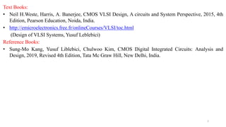
  • 1. 2 Text Books: • Neil H.Weste, Harris, A. Banerjee, CMOS VLSI Design, A circuits and System Perspective, 2015, 4th Edition, Pearson Education, Noida, India. • http://emicroelectronics.free.fr/onlineCourses/VLSI/toc.html (Design of VLSI Systems, Yusuf Leblebici) Reference Books: • Sung-Mo Kang, Yusuf Liblebici, Chulwoo Kim, CMOS Digital Integrated Circuits: Analysis and Design, 2019, Revised 4th Edition, Tata Mc Graw Hill, New Delhi, India.
  • 2. IntegratedCircuit-Moore’sLaw • Moore's law (In year 1975) is the observation that the number of transistors in an integrated circuit (IC) doubles about every two years. • Moore's law is an observation/empirical relationship and projection of a historical trend, rather than a law of physics. • The observation is named after Gordon Moore, the co-founder of Fairchild Semiconductor and former CEO of the Intel (Integrated Electronics). • The level of integration as measured by the number of logic gates in a monolithic chip has been steadily rising for almost three decades. Evolution of logic complexity in integrated circuits
  • 3. • Less area/volume and therefore, compactness • Less power consumption • Less testing requirements at system level • Higher reliability, mainly due to improved on-chip interconnects • Higher speed, due to significantly reduced interconnection length • Significant cost savings IntegratedCircuit–DesignObjectives/Performancemetrics
  • 4. VLSIDesignFlow-DesignPartitioning Flowchart of VLSI design flow Front end design (Involves gate level HDL-EDA tools) Back end design (Involves transistor level CAD tools) Architectural Design: User’s perspective, what does it do? Example: Instruction set, registers MIPS, x86, Alpha, PIC, ARM, … Functional Design Example: Single cycle, multcycle, pipelined, superscalar? Logic: how are functional blocks constructed Example: Ripple carry, carry lookahead, carry select adders Circuit: how are transistors used Example: Complementary CMOS, pass transistors, domino
  • 5. 5 VLSIDesignFlow • The design process, at various levels, is usually evolutionary in nature. • It starts with a given set of requirements. Initial design is developed and tested against the requirements. • When requirements are not met, the design has to be improved. • If such improvement is either not possible or too costly, then the revision of requirements and its impact analysis must be considered.
  • 6. • The Y-chart (first introduced by D. Gajski) shown in Figure illustrates a design flow for most logic chips, using design activities on three different axes (domains) which resemble the letter Y. • The Y-chart consists of three major domains, namely: • behavioral domain • structural domain • geometrical layout/Physical domain VLSIDesignFlow::Y-chart
  • 7. • Although the design process has been described in linear fashion for simplicity, in reality there are many iterations back and forth, especially between any two neighboring steps, and occasionally even remotely separated pairs. • Although top-down design flow provides an excellent design process control, in reality, there is no truly unidirectional top-down design flow. Both top-down and bottom-up approaches have to be combined. VLSIDesignFlow
  • 8. • The use of hierarchy, or “divide and conquer” technique involves dividing a module into sub- modules and then repeating this operation on the sub- modules until the complexity of the smaller parts becomes manageable. • This approach is very similar to the software case where large programs are split into smaller and smaller sections until simple subroutines, with well- defined functions and interfaces, can be written. • A hierarchy structure can be described in each domain (shown in Y-chart) separately. VLSIDesignHierarchy
  • 10. VLSIDesignHierarchy:: Conceptsof Regularity,ModularityandLocality The VLSI design hierarchy mush take care/satisfy of the following concepts. Regularity: The hierarchical decomposition of a large system should result in not only simple, but also similar blocks, as much as possible. Regularity usually reduces the number of different modules that need to be designed and verified, at all levels of abstraction. Modularity: The various functional blocks which make up the larger system must have well-defined functions and interfaces. Locality: Internal details remain at the local level. The concept of locality also ensures that connections are mostly between neighboring modules, avoiding long-distance connections as much as possible.
  • 11. VLSIDesignStyles • Standard IC • Application specific IC (ASIC) : Following are the various ASIC Design Styles
  • 12. VLSIDesignStyles::full-custom In full-custom style, the designer has many degrees of freedom to optimize a circuit design: • Adjust individual transistor dimensions (channel width, channel length, aspect ratio, etc.) to satisfy: • DC specifications (voltage levels, switching thresholds) • Transient specifications (delay times, rise- and fall-times) • Freely choose the most appropriate topology (placement and routing) for each circuit block. • Decide for the interconnection strategy between neighboring blocks. • Decide for the global distribution of power, ground and clock.
  • 13. VLSIDesignStyles::standardcell Each standard cell is pre-designed, with: • Same cell height for all elements in the library • Horizontal PWR and GND lines at the top and at the bottom • Fixed pin locations (inputs and outputs) “Routing" Between the cells
  • 14. VLSIDesignStyles::standardcell-Examples Every standard cell is pre-designed for different channel widths to facilitate current drive capability.
  • 15. VLSIDesignStyles::FPGA Field Programmable Gate Array (FPGA): • Fully fabricated FPGA chips containing thousands of logic gates or even more, with programmable interconnects, are available to users for their custom hardware programming to realize desired functionality. • This design style provides a means for fast prototyping and also for cost-effective chip design, especially for low-volume applications. • A typical field programmable gate array (FPGA) chip consists of I/O buffers, an array of configurable logic blocks (CLBs), and programmable interconnect structures. • The programming of the interconnects is implemented by programming of RAM cells whose output terminals are connected to the gates of MOS pass transistors.