
Recommandé
Contenu connexe
Tendances
Tendances (20)
Similaire à Micro-electro-mechanical Systems
Similaire à Micro-electro-mechanical Systems (20)
Plus de utpal sarkar
Plus de utpal sarkar (20)
Dernier
Dernier (20)
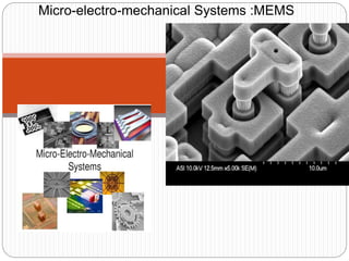
Micro-electro-mechanical Systems
- 3. What are MEMS? Micro-electromechanical Systems Common characteristics: Fabricated using micromachining Used for sensing, actuation or are passive structures Usually integrated with electronic circuitry for control and/or information processing
- 7. Linear Rack Gear Reduction Drive Linear Rack Gear Reduction Drive Triple-Piston Microsteam Engine
- 8. 3-D Micromachined Structures 2 dust mites on an optical shutter Deflection of laser light using a mirror
- 14. Outline • MEMS processing technologies – Bulk micromachining – Surface micromachining – LIGA (Lithographie, Galvanoformu ng, Abformung ) – Wafer bonding
- 15. SEM picture of an ant carrying a LIGA micro gear. This picture made the cover of Scientific American in November 1992 (G. Stix, Scientific American 267, 5 (1992))
- 16. Basic microfabrication technologies • Deposition – Chemical vapor deposition (CVD/PECVD/LPCVD) – Epitaxy – Oxidation – Evaporation – Sputtering – Spin-on methods • Etching – Wet chemical etching • Istropic • Anisotropic – Dry etching • Plasma etch • Reactive Ion etch (RIE, DRIE) • Patterning – Optical lithography – X-ray lithography
- 17. Etching
- 18. Chemicals used for etching
- 20. Anisotropic etching of silicon
- 22. Outline • Introduction • Applications – Passive structures – Sensors – Actuators • Future Applications • MEMS processing technologies – Bulk micromachining – Surface micromachining – LIGA – Wafer bonding • Thin film MEMS – Motivation – Microresonators • MEMS resources • Conclusions
- 23. Components Microelectronics: • “brain” that receives, processes, and makes decisions • data comes from microsensors Microsensors: • constantly gather data from environment • pass data to microelectronics for processing • can monitor mechanical, thermal, biological, chemical optical, and magnetic readings Microactuator: • acts as trigger to activate external device • microelectronics will tell microactuator to activate device Microstructures: • extremely small structures built onto surface of chip • built right into silicon of MEMS
- 24. Fabrication Processes Deposition: • deposit thin film of material (mask) anywhere between a few nm to 100 micrometers onto substrate • physical: material placed onto substrate, techniques include sputtering and evaporation • chemical: stream of source gas reacts on substrate to grow product, techniques include chemical vapor deposition and atomic layer deposition • substrates: silicon, glass, quartz • thin films:polysilicon, silicon dioxide, silicon nitride, metals, polymers
- 25. Patterning: • transfer of a pattern into a material after deposition in order to prepare for etching • techniques include some type of lithography, photolithography is common Etching: • wet etching: dipping substrate into chemical solution that selectively removes material • process provides good selectivity, etching rate of target material higher that mask material • dry etching: material sputtered or dissolved from substrate with plasma or gas variations • choosing a method: desired shapes, etch depth and uniformity, surface roughness, process compatibility, safety, cost, availability, environmental impact
- 26. Fabrication Methods Bulk Micromachining: • oldest micromachining technology • technique involves selective removal of substrate to produce mechanical components • accomplished by physical or chemical process with chemical being used more for MEMS production • chemical wet etching is popular because of high etch rate and selectivity • isotropic wet etching: etch rate not dependent on crystallographic orientation of substrate and etching moves at equal rates in all directions • anisotropic wet etching: etch rate is dependent on crystallographic orientation of substrate
- 28. Bulk micromachining Anisotropic etching of silicon Etchant 111 100 etch etch r r Selectivity to p + - Si Disadvantages Potassium Hydroxide (KOH) 100 Yes -Highly corrosive -Not CMOS compatible Tetramethyl ammonium hydroxide (TMAH) 30-50 yes -formation of pyramidal hillocks at bottom of cavity Ethylenediamine pyrochatechol (EDP) 35 Yes -carcinogenic vapors
- 29. Bulk micromachining Anisotropic etch of {100} Si 54.74º 111 a 0.707a
- 31. Surface Micromachining: • process starts with deposition of thin-film that acts as a temporary mechanical layer (sacrificial layer) • device layers are constructed on top • deposition and patterning of structural layer • removal of temporary layer to allow movement of structural layer • benefits: variety of structure, sacrificial and etchant combinations, uses single-sided wafer processing • allows higher integration density and lower resultant per die cost compared to bulk micromachining • disadvantages: mechanical properties of most thin-films are usually unknown and reproducibility of their mechanical properties
- 33. Sacrificial Layer Deposition and Patterning Structural Layer Deposition and Patterning Sacrificial Layer Removal d=1 m; h=500 nm; b=10 m Lmax(bridge) ~ 60 m ; Lmax(cantilever) ~ 30 m Surface micromachining on glass
- 34. Surface Micromachining Most commonly used materials for surface micromachining: • substrate: silicon • sacrificial material: SiO2 or phosphosilicate glass (PSG) • structural material: polysilicon Substrates Sacrificial Structural Glass Plastic metals Polymer Metals silicon nitride Thin film silicon (a-Si:H, c-Si) silicon nitrides Silicon carbide Metals polymers bilayer composites Alternative materials
- 35. Wafer Bonding: • Method that involves joining two or more wafers together to create a wafer stack • Three types of wafer bonding: direct bonding, anodic bonding, and intermediate layer bonding • All require substrates that are flat, smooth, and clean in order to be efficient and successful High Aspect Ratio Fabrication (Silicon): • Deep reactive ion etching (DRIE) • Enables very high aspect ratio etches to be performed into silicon substrates • Sidewalls of the etched holes are nearly vertical • Depth of the etch can be hundreds or even thousands of microns into the silicon substrate.
- 36. • Much smaller area • Cheaper than alternatives ○ In medical market, that means disposable • Can be integrated with electronics (system on one chip) • Speed: ○ Lower thermal time constant ○ Rapid response times(high frequency) • Power consumption: ○ low actuation energy ○ low heating power Benefits/Tradeoffs • Imperfect fabrication techniques • Difficult to design on micro scales
- 38. Where Are MEMS? Smartphones, tablets, cameras, gaming devices, and many other electronics have MEMS technology inside of them http://www.chipworks.com/en/technical-competitive-analysis/resources/blog/inside-the-samsung-galaxy-s5/
- 39. • Sensors & Actuators • 3 main types of transducers: o Capacitive o Piezoelectric o Thermal • Additionally: Microfluidic MEMS Operation
- 40. MEMS Accelerometer Inertial Sensors MEMS Gyroscope
- 41. Biomedical Applications Blood Pressure sensor on the head of a pin ● Usually in the form of pressure sensors ○ Intracranial pressure sensors ○ Pacemaker applications ○ Implanted coronary pressure measurements ○ Intraocular pressure monitors ○ Cerebrospinal fluid pressure sensors ○ Endoscope pressure sensors ○ Infusion pump sensors ● Retinal prosthesis ● Glucose monitoring & insulin delivery ● MEMS tweezers & surgical tools ● Cell, antibody, DNA, RNA enzyme measurement devices
- 42. In the Car
- 43. Applications: Sensors Pressure sensor: • Piezoresistive sensing • Capacitive sensing • Resonant sensing Application examples: • Manifold absolute pressure (MAP) sensor • Disposable blood pressure sensor (Novasensor)
- 45. Piezoresistive Pressure Sensors Wheatstone Bridge configuration Illustration from “An Introduction to MEMS Engineering”, N. Maluf
- 47. Piezoresistive Pressure Sensors Pressure Piezoresistive elements SiO2 n type p type Glass
- 48. Bulk micromachining: Pressure sensors Piezoresistive elements SiO2 N type epitaxial laye P type Glass
- 50. MEMS Devices
- 51. MEMS devices
- 52. • Optical MEMS o Ex: optical switches, digital micromirror devices (DMD), bistable mirrors, laser scanners, optical shutters, and dynamic micromirror displays • RF MEMS o Smaller, cheaper, better way to manipulate RF signals o Reliability is issue, but getting there Additional Applications
- 53. Summary/Conclusion Micro-Electro-Mechanical Systems are 1-100 micrometer devices that convert electrical energy to mechanical energy and vice-versa. The three basic steps to MEMS fabrication are deposition, patterning, and etching. Due to their small size, they can exhibit certain characteristics that their macro equivalents can’t. MEMS produce benefits in speed, complexity, power consumption, device area, and system integration. These benefits make MEMS a great choice for devices in numerous fields.
- 54. References • "What Is MEMS Technology?" What Is MEMS Technology? N.p., n.d. Web. 28 Apr. 2014. • "Fabricating MEMS and Nanotechnology." Fabricating MEMS and Nanotechnology. N.p., n.d. Web. 28Apr. 2014. • D. J. Nagel and M. E. Zaghloul,“MEMS: Micro Technology, MegaImpact,” IEEE Circuits Devices Mag.,pp. 14-25, Mar. 2001. • K. W. Markus and K. J. Gabriel,“MEMS: The Systems Function Revolution,” IEEE Computer, pp. 25-31, Oct. 1990. • K. W. Markus, “Developing Infrastructure to Mass-Produce MEMS,” IEEE Comput. Sci. Eng., Mag., pp. 49-54, Jan. 1997. • M. E. Motamedi, "Merging Micro-optics with Micromechanics: Micro-Opto-Electro-Mechanical (MOEM) devices", Critical Reviews of Optical Science and Technology, V. CR49, SPIE Annual Meeting, Proceeding of Diffractive and Miniaturized Optics, page 302-328, July, 1993 • http://seor.gmu.edu/student_project/syst101_00b/team07/components.html • https://www.mems-exchange.org/MEMS/fabrication.html • http://www-bsac.eecs.berkeley.edu/projects/ee245/Lectures/lecturepdfs/Lecture2.BulkMicromachining.pdf Images • http://www.docstoc.com/docs/83516847/What-are-MEMS • http://seor.gmu.edu/student_project/syst101_00b/team07/images/MEMScomponents2.gif • http://www.empf.org/empfasis/2010/December10/images/fig3-1.gif • http://pubs.rsc.org/en/content/articlehtml/2003/AN/B208563C#sect274 • http://www.photonics.com/images/Web/Articles/2008/11/1/thumbnail_35519.jpg • https://www.memsnet.org/mems/fabrication.html
- 55. 5 Key Concepts 1. MEMS are made up of microelectronics, microactuators, microsensors, and microstructures. 2. The three basic steps to MEMS fabrication are: deposition, patterning, and etching. 3. Chemical wet etching is popular because of high etch rate and selectivity. 4. 3 types of MEMS transducers are: capacitive, thermal, and piezoelectric. 5. The benefits of using MEMS: speed, power consumption, size, system integration(all on one chip).