

Recommandé
Contenu connexe
Tendances
Tendances (20)
En vedette
En vedette (18)
Similaire à Power Supply Management
Similaire à Power Supply Management (20)
Power Supply Management
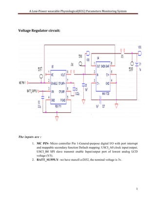
- 1. A Low-Power wearable Physiological(ECG) Parameters Monitoring System Voltage Regulator circuit: The inputs are : 1. MC PIN- Micro controller Pin 1-General-purpose digital I/O with port interrupt and mappable secondary function Default mapping: USCI_A0 clock input/output; USCI_B0 SPI slave transmit enable Input/output port of lowest analog LCD voltage (V5). 2. BATT_SUPPLY- we have maxell cr2032, the nominal voltage is 3v. 1
- 2. A Low-Power wearable Physiological(ECG) Parameters Monitoring System REG 711: The REG711 is a switched capacitor voltage converter, which produces a regulated, low ripple output voltage from an unregulated input voltage. A wide input supply voltage of 1.8V to 5.5V makes the REG711 ideal for a variety of battery sources, such as single cell Li-Ion, or two and three cell Nickel or Alkaline based chemistries. The input voltage may vary above and below the output voltage and the output will remain in regulation. It works equally well for step up or down without the need for an inductor, providing low EMI DC/DC conversion. The high switching frequency allows the use of small surface-mount capacitors, saving board space and reducing cost. The REG711 is thermally protected and current limited, protecting the load and the regulator during fault conditions. Typical ground pin current (quiescent current) is 1mA at full load, 60uA with no load, and less than 1uA in shutdown mode. This regulator comes in a thin MSOP-8 package with a component height of less than 1.1mm. MAX 1720: The ultra-small MAX1720 monolithic, CMOS charge-pump inverters accept input voltages ranging from +1.5V to +5.5V. The MAX1720 operates at 12kHz.High efficiency, small external components, and logic-controlled shutdown make these devices ideal for both battery-powered and board-level voltage conversion applications. Oscillator control circuitry and four power MOSFET switches are included on- chip. A typical MAX1719/ MAX1720/MAX1721 application is generating a -5V supply from a +5V logic supply to power analog circuitry. All three parts come in a 6-pin SOT23 package and can deliver a continuous 25mA output current. The outputs are : 1.Vss: Voltage Source,Source Neative Voltage supply = -2.5V. 2.Vdd: Voltage Drain, Drain Positive Voltage Supply = +2.5V. J4,J5 are the Jumpers Plugs. MCPIN 1 is connected to the ENABLE pin in the REG711 and SHDN BAR (6th) pin in the MAX 1720. Battery supply is given to the vin pin in the REG711. We get Vdd when the jumper J4 is closed,and J5 is closed we get Vss. 2
- 3. A Low-Power wearable Physiological(ECG) Parameters Monitoring System Power supply to ECG sensors: Supply Vdd,Vss as input to the PS25201A,PS25201A sensors and connect with a common ground. We get EPIC sensor 1,EPIC Sensor 2 as outputs with noise. Here Vdd=+2.5V, Vss=-2.5V 3
- 4. A Low-Power wearable Physiological(ECG) Parameters Monitoring System PS25201A: Plessey Semiconductors Electric Potential Integrated Circuit (EPIC) product line targets a range of applications. The PS25201A is an ultra high impedance solid state ECG (electrocardiograph) sensor. It can be used as a dry contact ECG sensor without the need for potentially dangerous low impedance circuits across the heart. The resolution available is as good as or better than conventional wet electrodes. The device uses active feedback techniques to both lower the effective input capacitance of the sensing element (Cin) and boost the input resistance (Rin). These techniques are used to realise a sensor with a frequency response suitable for both diagnostic and monitoring ECG applications. Fig: Internal circuit of EPIC ECG Sensor 4
- 5. A Low-Power wearable Physiological(ECG) Parameters Monitoring System APPLICATION OF THE ECG SENSOR: Because of the large coupling capacitance to the body (around 250pF) the EPIC sensor’s internal electrometer can be used in differential mode to recover true surface potential ECG signals from the surface of the skin. A typical ECG signal at the surface of the skin is 1mV p-p. DRL and INA Fig:Instrumentation Amplifier 5
- 6. A Low-Power wearable Physiological(ECG) Parameters Monitoring System Assign the EPIC Sensor OUT1,OUT2 to the INA 126 amplifier. Give Vdd,Vss Supply to the INA 126 and also for AD8505. We get INA OUT from the INA126 Instrumentation Amplifier. Connect AD8505 OUT pin to the Human Body. INA126: The INA126 and INA2126 are precision instrumentation amplifiers for accurate, low noise differential signal cquisition. Their two-op-amp design provides excellent performance with very low quiescent current (175mA/chan.). This,combined with wide operating voltage range of ±1.35V to ±18V, makes them ideal for portable instrumentation and data acquisition systems. Gain can be set from 5V/V to 10000V/V with a single external resistor. Laser trimmed input circuitry provides low offset voltage (250mV max), low offset voltage drift (3mV/°C max) and excellent common-mode rejection. Single version package options include 8-pin plastic DIP, SO-8 surface mount, and fine-pitch MSOP-8 surface-mount. Dual version is available in the space-saving SSOP-16 finepitch surface mount, SO-16, and 16-pin DIP. All are specified for the –40°C to +85°C industrial temperature range. APPLICATIONS Industrial sensor amplifier: Bridge, RTD, Thermocouple Physiological amplifier: ECG, EEG, EMG Multi-channel data acquisition Portable, battery operated systems LOW VOLTAGE OPERATION The INA126/2126 can be operated on power supplies as low as ±1.35V. Performance remains excellent with power supplies ranging from ±1.35V to ±18V. Most parameters vary only slightly throughout this supply voltage range—see typical performance curves. Operation at very low supply voltage requires careful attention to ensure that the ommonmode voltage remains within its linear range. See ―Input Common-Mode Voltage Range.‖ The INA126/2126 can be operated from a single power supply with careful attention to input common-mode range, output voltage swing of both op amps and the voltage applied to the Ref terminal. Figure 4 shows a bridge amplifier circuit operated from a single +5V power supply. The bridge provides an input common-mode voltage near 2.5V, with a relatively small differential voltage. 6
- 7. A Low-Power wearable Physiological(ECG) Parameters Monitoring System NOTCH FILTER: This Filter is used to reduce the Noise. Assign INA OUT to the FILTER INPUT and give Vss,Vdd supply for the AD8506 Amplifier. We get ECG signal without Noise(FILTER OUTPUT) AD8506: The AD8506/AD8508 are dual and quad micropower amplifiers featuring rail-to- rail input and output swings while operating from a single 1.8 V to 5 V power supply or from dual ±0.9 V to ±2.5 V power supplies. Using a new circuit technology, these low cost amplifiers offer zero input crossover distortion (excellent PSRR and CMRR performance) and very low bias current, while operating with a supply current of less than 20 μA per amplifier. This amplifier family offers the lowest noise in its power class. This combination of features makes the AD8506/AD8508 amplifiers ideal choices for battery-powered applications because they minimize errors due to power supply voltage variations over the lifetime of the battery and maintain high CMRR even for a rail-to-rail input op amp. Remote battery-powered sensors, handheld instrumentation and 7
- 8. A Low-Power wearable Physiological(ECG) Parameters Monitoring System consumer equipment, hazard detection (for example, smoke, fire, and gas), and patient monitors can benefit from the features of the AD8506/AD8508 amplifiers. The AD8506/AD8508 are specified for both the industrial temperature range of −40°C to +85°C and the extended industrial temperature range of −40°C to +125°C. The AD8506 dual amplifi-er is available in 8-lead MSOP and 8-ball WLCSP packages. The AD8508 quad amplifier is available in 14-lead TSSOP and 14-ball WLCSP packages. The AD8506/AD8508 are members of a growing series of zero crossover op amps offered by Analog Devices, Inc., including the ADA4505-2/ADA4505-4, which also operates from a single 1.8 V to 5 V supply or from dual ±0.9 V to ±2.5 V power supplies. 8