SlideShare une entreprise Scribd logo
1  sur  19
1. Convert the following hexadecimal numbers to base 10:

   a.   1458

Answer;
14516=(b)10
Where b is the number of base 10;
Therefore;
1x162+4x161+5x160
1X16X16+4X16+5X1
256+64+5
=32510

b .A2C1
Answer;

A2C116=(b)10
Where b is the number of base 10;
Therefore;
AX163+2X162+CX161+1X160
10X16X16X16+2X16X16+12X16+1X1
40960+512+192+1
=4166510

Q2: Universal gate these are gate that are used to design other gates. They are gate that use to
implement other high gate. They are gate that are used to carry out or express Boolean expression. The
NAND gate is a universal gate in the sense that any Boolean function can be implemented by NAND
gates.The NAND gates are one of the two basic logic gates (the other being NOR logic gates) from which
any other logic gates can be built. Due to this property, NAND and NOR gates are sometimes called
"universal gates". However, modern integrated circuits are not constructed exclusively from a single
type of gate.

A universal gate is a gate which can implement any Boolean function without need to use any other
gate type. The NAND and NOR gates are universal gates.
In practice, this is advantageous since NAND and NOR gates are economical and easier to fabricate
and are the basic gates used in all IC digital logic families. In fact, an AND gate is typically
implemented as a NAND gate followed by an inverter not the other way around!! Likewise, an OR
gate is typically implemented as a NOR gate followed by an inverter not the other way around!!


NAND Gate:
The NAND gate represents the complement of the AND operation. Its name is an abbreviation of
NOT AND. The graphic symbol for the NAND gate consists of an AND symbol with a bubble on the
output, denoting that a complement operation is performed on the output of the AND gate.

The truth table and the graphic symbol of NAND gate is shown below;


NAND Gate is a Universal Gate;

To prove that any Boolean function can be implemented using only NAND gates, we will show that
the AND, OR, and NOT operations can be performed using only these gates.

Implementing an Inverter Using only NAND Gate;

1. All NAND input pins connect to the input signal Agives an output A’.


2. One NAND input pin is connected to the input signal A while all other input pins are connected to
logic 1. The output will be A’.
Implementing an AND using only NAND GATE;

3. An AND gate can be replaced by NAND with its output complemented by a NAND gate inverter.


Implementing OR Using only NAND Gates;
4. An OR gate can be replaced by NAND with it’s input complemented by a NAND gate inverter.


Thus ,the NAND gate is a unversal gate since it can implement the AND,OR and NOT functions.
NOR Gate:
The NOR gate represents the complement of the OR operation. Its name is an abbreviation of NOT
OR. The graphic symbol for the NOR gate consists of an OR symbol with a bubble on the output,
denoting that a complement operation is performed on the output of the OR gate.
The truth table and the graphic symbol of NOR gate as show
below;


The truth table clearly shows that the NOR operation is the complement of the OR.


NOR Gate is a Universal Gate:
To prove that any Boolean function can be implemented using only NOR gates, we will show that
the AND, OR, and NOT operations can be performed using only these gates.

Implementing and inverter using NOR gate;
   1. All NOR input pins connect to the input signal A gives an output A’.


   2. One NOR input pin is connected to the input signal A while all other input pins are connected
      to logic 0. The output will be A’.
Implementing OR Using only NOR Gates;

    1. The OR is replaced by a NOR gate with it's output complemented by a NOR gate inverter.


Implementing AND Using only NOR Gates;
  2. The NAND gates is replaced by a NOR gate with all it's inputs complemented by NOR
     gates inverters.


1
Thus, the NOR gate is a universal gate since it can implement the AND, OR and
NOT functions.

The reason why they are called universal gate;
    1. Universal gates are the ones from which we can design other gates also. foreg. NAND and
       NOR gates. they help in forming the uniformity in the circuits.

    2. NAND and NOR both are called as universal gate. You can built any circuit or design using
       either NAND or NOR, this will be so flexible to fabricate any circuit in a single chip
    3. They are less expensive to construct


5. Draw and explain the working of JK, S-R, and D flip flops.


JK flip-flop
A circuit symbol for a positive-edge-triggered JK flip-flop


JK flip-flop timing diagram

The JK flip-flop augments the behavior of the SR flip-flop (J=Set, K=Reset) by interpreting the
S = R = 1 condition as a "flip" or toggle command. Specifically, the combination J = 1, K = 0 is a
command to set the flip-flop; the combination J = 0, K = 1 is a command to reset the flip-flop;
and the combination J = K = 1 is a command to toggle the flip-flop, i.e., change its output to the
logical complement of its current value. Setting J = K = 0 does NOT result in a D flip-flop, but
rather, will hold the current state. To synthesize a D flip-flop, simply set K equal to the
complement of J. Similarly, to synthesize a T flip-flop, set K equal to J. The JK flip-flop is
therefore a universal flip-flop, because it can be configured to work as an SR flip-flop, a D flip-
flop, or a T flip-flop.

The characteristic equation of the JK flip-flop is:


and the corresponding truth table is:

        JK Flip Flop operation[28]
Characteristic table   Excitation table
J K Qnext Comment Q Qnext J K Comment
0 0 Q hold state 0 0 0 X No change
0 1 0       reset    0 1 1X         Set
1 0 1        set     1 0 X 1 Reset
1 1 Q      toggle 1 1 X 0 No change
S-R NOR latch


An SR latch, constructed from a pair of cross-coupled NOR gate (an animated picture). Red and black
mean logical '1' and '0', respectively.

When using static gates as building blocks, the most fundamental latch is the simple S-R latch,
where S and R stand for set and reset. It can be constructed from a pair of cross-coupled
NORlogic gates. The stored bit is present on the output marked Q.

While the S and R inputs are both low, feedback maintains the Q and Q outputs in a constant
state, with Q the complement of Q. If S (Set) is pulsed high while R (Reset) is held low, then the
Q output is forced high, and stays high when S returns to low; similarly, if R is pulsed high while
S is held low, then the Q output is forced low, and stays low when R returns to low.

        S-R Flip Flop operation

Characteristic table Excitation table

S R Qnext    Action   Q Qnext S R

00 Q        hold state 0    0     0 x

01 0          reset   0     1     1 0

10 1           set    1     0     0 1

1 1 X not allowed 1         1     X 0


The R = S = 1 combination is called a restricted combination or a forbidden state because, as
both NOR gates then output zeros, it breaks the logical equation Q = not Q. The combination is
also inappropriate in circuits where both inputs may go low simultaneously (i.e. a transition from
restricted to keep). The output would lock at either 1 or 0 depending on the propagation time
relations between the gates (a race condition). In certain implementations, it could also lead to
longer ringings (damped oscillations) before the output settles, and thereby result in
undetermined values (errors) in high-frequency digital circuits. Although this condition is usually
avoided, it can be useful in some applications.

To overcome the restricted combination, one can add gates to the inputs that would convert
(S,R) = (1,1) to one of the non-restricted combinations. That can be:

       Q = 1 (1,0) – referred to as an S-latch
       Q = 0 (0,1) – referred to as an R-latch
       Keep state (0,0) – referred to as an E-latch

Alternatively, the restricted combination can be made to toggle the output. The result is the JK
latch.

Characteristic: Q+ = R'Q + R'S or Q+ = R'Q + S


Gated SR latch


A gated SR latch circuit diagram constructed from NOR gates.

A synchronous SR latch (sometimes clocked SR flip-flop) can be made by adding a second level
of NAND gates to the inverted SR latch (or a second level of AND gates to the direct SR latch).
The extra gates further invert the inputs so the simple SR latch becomes a gated SR latch (and a
simple SR latch would transform into a gated SR latch with inverted enable).

With E high (enable true), the signals can pass through the input gates to the encapsulated latch;
all signal combinations except for (0,0) = hold then immediately reproduce on the (Q,Q) output,
i.e. the latch is transparent.

With E low (enable false) the latch is closed (opaque) and remains in the state it was left the last
time E was high.

The enable input is sometimes a clock signal, but more often a read or write strobe.
Gated S-R latch operation


 E/C                Action


  0         No action (keep state)

                                           Symbol for a gated SR latch
  1    The same as non-clocked SR latch


Gated D latch


A D-type transparent latch based on an SR NAND latch


A gated D latch based on an SR NOR latch

This latch exploits the fact that, in the two active input combinations (01 and 10) of a gated SR
latch, R is the complement of S. The input NAND stage converts the two D input states (0 and 1)
to these two input combinations for the next SR latch by inverting the data input signal. The low
state of the enable signal produces the inactive "11" combination. Thus a gated D-latch may be
considered as a one-input synchronous SR latch. This configuration prevents application of the
restricted input combination. It is also known as transparent latch, data latch, or simply gated
latch. It has a data input and an enable signal (sometimes named clock, or control). The word
transparent comes from the fact that, when the enable input is on, the signal propagates directly
through the circuit, from the input D to the output Q.
Transparent latches are typically used as I/O ports or in asynchronous systems, or in synchronous
two-phase systems (synchronous systems that use a two-phase clock), where two latches
operating on different clock phases prevent data transparency as in a master–slave flip-flop.

Latches are available as integrated circuits, usually with multiple latches per chip. For example,
74HC75 is a quadruple transparent latch in the 7400 series.


         Gated D latch truth table


 E/C      D      Q        Q      Comment


   0      X     Qprev    Qprev   No change


   1      0          0    1        Reset     Symbol for a gated D latch


   1      1          1    0          Set


The truth table shows that when the enable/clock input is 0, the D input has no effect on the
output. When E/C is high, the output equals D.


D flip-flop


D flip-flop symbol

The D flip-flop is widely used. It is also known as a data or delay flip-flop.

The D flip-flop captures the value of the D-input at a definite portion of the clock cycle (such as
the rising edge of the clock). That captured value becomes the Q output. At other times, the
output Q does not change. The D flip-flop can be viewed as a memory cell, a zero-order hold, or
a delay line.
Truth table:

            Clock     D Qnext

        Rising edge 0       0

        Rising edge 1       1

         Non-Rising X Q


('X' denotes a Don't care condition, meaning the signal is irrelevant)

Most D-type flip-flops in ICs have the capability to be forced to the set or reset state (which
ignores the D and clock inputs), much like an S-R flip-flop. Usually, the illegal S = R = 1
condition is resolved in D-type flip-flops. By setting S = R = 0, the flip-flop can be used as
described above.

           Inputs       Outputs

         S R D >       Q        Q'

         0 1 X X        0       1

         1 0 X X        1       0

         1 1 X X        1       1


4-bit serial-in, parallel-out (SIPO) shift register
These flip-flops are very useful, as they form the basis for shift registers, which are an essential
part of many electronic devices. The advantage of the D flip-flop over the D-type "transparent
latch" is that the signal on the D input pin is captured the moment the flip-flop is clocked, and
subsequent changes on the D input will be ignored until the next clock event. An exception is
that some flip-flops have a "reset" signal input, which will reset Q (to zero), and may be either
asynchronous or synchronous with the clock.

The above circuit shifts the contents of the register to the right, one bit position on each active
transition of the clock. The input X is shifted into the leftmost bit position.

Classical positive-edge-triggered D flip-flop


A positive-edge-triggered D flip-flop

This clever circuit consists of two stages implemented by S-R NAND latches. The input stage
(the two latches on the left) processes the clock and data signals to ensure correct input signals
for the output stage (the single latch on the right). If the clock is low, both the output signals of
the input stage are high regardless of the data input; the output latch is unaffected and it stores
the previous state. When the clock signal changes from low to high, only one of the output
voltages (depending on the data signal) goes low and sets/resets the output latch: if D = 0, the
lower output becomes low; if D = 1, the upper output becomes low. If the clock signal continues
staying high, the outputs keep their states regardless of the data input and force the output latch
to stay in the corresponding state as the input logical zero remains active while the clock is high.
Hence the role of the output latch is to store the data only while the clock is low.

The circuit is closely related to the gated D latch as both the circuits convert the two D input
states (0 and 1) to two input combinations (01 and 10) for the output S-R latch by inverting the
data input signal (both the circuits split the single D signal in two complementary S and R
signals). The difference is that in the gated D latch simple NAND logical gates are used while in
the positive-edge-triggered D flip-flop SR NAND latches are used for this purpose. The role of
these latches is to "lock" the active output producing low voltage (a logical zero); thus the
positive-edge-triggered D flip-flop can be thought of as a gated D latch with latched input gates.
Q6. Give any two applications of a shift register.
        Answer

   1.      Very effective for sequence detectors.
   2.      Shift register are often used as the state register in a sequential device.


Q7. Explain the working principle of a 4 bit Johnson counter with a neat
diagram.
        Answer.


The demonstration above initially implements only the legitimate counting sequence of the Johnson
counter. To allow for all possible illegal combinations and show how they get straightened out, we
would need 66 separate images for the over lays, and each is about 6.5k bytes in size. That’s a bit much
to ask of many users. however, you can see the count correction gates operating at the bottom of the
counter, and see how they work. The D input to flip-flop C is not directly driven from the B output.
Rather , A’ and C’ are added together, and that combination is NO Red with B’, as a result, improper bits
reaching flip-flop B get blocked, and flip-flop C can only take on the correct state to reinstate the correct
shifting sequence. To see this in action, you can click on any of the individual flip-flops in the figure. This
will force a load of all remaining images and change the state of the selected flip-flop without applying a
clock pulse. Then you can watch the behavior of the counter as it removes improper counting
sequences. Remember that the download of the additional images may take some time, so please be
patient. You can only identify an illegal counting sequence because more than one output will be high
(logic 1). Since each output is enabled by a transition from 0 to 1 or from 1 to 0 in a specific position in
the counter, more than one transition will produce more than one output, which is illegal in this context.
Also note that in order to repeatedly invert the shifting bits as they start from flip-flop A, the E' output is
fed back to the A flip-flop's D input. This shift does not constitute a second transition here; only when all
bits are the same does this appear as a transition. Of course, these must necessarily be edge-triggered
flip-flops clocked simultaneously. The Reset inputs are asynchronous and override the clocking signal. In
addition, the CMOS ICs that serve as the model for this demonstration change state on the rising edge of
the clock, so this model does the same. The COUT signal is the Carry Out, which is a symmetrical square
wave at one-tenth of the incoming Clock signal frequency. It is quite suitable for clocking a second
counter of the same type, to form a multiple-digit decimal counter.


Q8.     Explain temperature and weather forecast system with a neat circuit diagram.

Answer;
Hardware calibration is simply a matter of setting the offset voltage to the value listed in table 1 for your
altitude. A jumper on the input of the DS2438 allows the use of the DS2438 to measure the offset. Put the
jumper in the A-C position and using the iButton Viewer for the DS2438, set the voltage to the table
value using the 25-turn pot. Once it’s set, put the jumper in the A-B position to read pressure.
         For altitudes in between the values listed in the table, simple interpolation will give accurate
results. An Excel spreadsheet will be also available online to calculate intermediate values. Software:
Routines currently exist to measure the DS2438s Vad voltage. Once this voltage is measured, the
pressure is calculated using: Press = slope * Vad + intercept Where the slope and intercept are the
values listed in table 1 for your altitude. The prototype code I used had an external text file to store the
slope and intercept values. This allows the user to edit the file to fine-tune the calibration if desired.
Fine-tuning can be accomplished by monitoring the pressure and comparing it with a known reference
source, such as a nearby airport or NOAA weather. Start by adjusting the intercept. When the reference
station indicates a pressure near mid-scale (30.00 inHg), adjust the software intercept value until your
weather station matches. Now monitor the pressure extremes to determine if the slope needs
adjustment. An Excel spreadsheet will be available as an aid.


Q10.            Write a short note on ADC.

Answer;

ADC
An analog-to-digital converter (abbreviated ADC, A/D or A to D) is an electronic integrated circuit,
which converts continuous signals to discrete digital numbers.
 Typically, an ADC is an electronic device that converts an input analog voltage (or current) to a digital
number. The digital output may be using different coding schemes, such as binary, Gray code or two's
complement binary. However, some non-electronic or only partially electronic devices, such as rotary
encoders, can also be considered ADCs.


Working Principle & Circuits of Analog to Digital Concepts

Resolution

The resolution of the converter indicates the number of discrete values it can produce over the range of
analog values. The values are usually stored electronically in binary form, so the resolution is usually
expressed in bits. In consequence, the number of discrete values available, or "levels", is usually a power
of two. For example, an ADC with a resolution of 8 bits can encode an analog input to one in 256
different levels, since 28 = 256. The values can represent the ranges from 0 to 255 (i.e. unsigned integer)
or from -128 to 127 (i.e. signed integer), depending on the application. Resolution can also be defined
electrically, and expressed in volts. The voltage resolution of an ADC is equal to its overall voltage
measurement range divided by the number of discrete intervals as in the formula: Where: Q is
resolution in volts per step (volts per output code), N E 2 E Q FSR M FSR

EFSR is the full scale voltage range = VRefHi − VRefLo and M is the ADC's resolution in bits. The number
of intervals is given by the number of available levels (output codes), which is: N = 2M Some examples
may help:
Example: Full scale measurement range = 0 to 10 volts ADC resolution is 12 bits: 212 = 4096
quantization levels (codes) ADC voltage resolution is: (10V - 0V) / 4096 codes = 10V / 4096 codes
0.00244 volts/code 2.44 mV/code


Response type


Linear ADCs

Most ADCs are of a type known as linear, although analog-to-digital conversion is an inherently non-
linear process (since the mapping of a continuous space to a discrete space is a piecewise-constant and
therefore non-linear operation). The term linear as used here means that the range of the input values
that map to each output value has a linear relationship with the output value, i.e., that the output value
k is used for the range of input values from m(k + b) to m(k + 1 + b), where m and b are constants. Here
b is typically 0 or −0.5. When b = 0, the ADC is referred to as mid-rise, and when b = −0.5 it is referred to
as mid-tread.


Non-linear ADCs If the probability density function of a signal being digitized is uniform, then the
signal-to-noise ratio relative to the quantization noise is the best possible. Because of this, it's usual to
pass the signal through its cumulative distribution function (CDF) before the quantization. This is good
because the regions that are more important get quantized with a better resolution. In the dequantization
process, the inverse CDF is needed. This is the same principle behind the commanders used in some tape-
recorders and other communication systems, and is related to entropy maximization. (Never confuse
commanders with compressors!) For example, a voice signal has a Laplacian distribution. This means that
the region around the lowest levels, near 0, carries more information than the regions with higher
amplitudes. Because of this, logarithmic ADCs are very common in voice communication systems to
increase the dynamic range of the represent able values while retaining fine-granular fidelity in the low-
amplitude region

Accuracy An ADC has several sources of errors. Quantization error and (assuming the ADC is intended
to be linear) non-linearity is intrinsic to any analog-to-digital conversion. There is also a so-called
aperture error which is due to a clock jitter and is revealed when digitizing a time-variant signal (not a
constant value). These errors are measured in a unit called the LSB, which is an abbreviation for least
significant bit. In the above example of an eight-bit ADC, an error of one LSB is 1/256 of the full signal
range, or about 0.4%.

Quantization error Quantization error is due to the finite resolution of the ADC, and is an unavoidable
imperfection in all types of ADC. The magnitude of the quantization error at the sampling instant is
between zero and half of one LSB. In the general case, the original signal is much larger than one LSB.
When this happens, the quantization error is not correlated with the signal, and has a uniform distribution.
Its RMS value is the standard deviation of this distribution, given by In the eight-bit ADC example, this
represents 0.113% of the full signal range.
At lower levels the quantizing error becomes dependent of the input signal, resulting in distortion. This
distortion is created after the anti-aliasing filter.
Sampling rate

The analog signal is continuous in time and it is necessary to convert this to a flow of digital values. It is
therefore required to define the rate at which new digital values are sampled from the analog signal. The
rate of new values is called the sampling rate or sampling frequency of the converter. A continuously
varying band limited signal can be sampled (that is, the signal values at intervals of time T, the sampling
time, are measured and stored) and then the original signal can be exactly reproduced from the discrete-
time values by an interpolation formula. The accuracy is limited by quantization error. However, this
faithful reproduction is only possible if the sampling rate is higher than twice the highest frequency of the
signal. This is essentially what is embodied in the Shannon-Nyquist sampling theorem. Since a practical
ADC cannot make an instantaneous conversion, the input value must necessarily be held constant during
the time that the converter performs a conversion (called the conversion time). An input circuit called a
sample and hold performs this task – in most cases by using a capacitor to store the analogue voltage at
the input, and using an electronic switch or gate to disconnect the capacitor from the input. Many ADC
integrated circuits include the sample and hold subsystem internally.


Aliasing All ADCs work by sampling their input at discrete intervals of time. Their output is therefore an
incomplete picture of the behavior of the input. There is no way of knowing, by looking at the output,
what the input was doing between one sampling instant and the next. If the input is known to be changing
slowly compared to the sampling rate, then it can be assumed that the value of the signal between two
sample instants was somewhere between the two sampled values. If, however, the input signal is changing
fast compared to the sample rate, then this assumption is not valid.
If the digital values produced by the ADC are, at some later stage in the system, converted back to
analog values by a digital to analog converter or DAC, it is desirable that the output of the DAC be a
faithful representation of the original signal. If the input signal is changing much faster than the sample
rate, then this will not be the case, and spurious signals called aliases will be produced at the output of
the DAC. The frequency of the aliased signal is the difference between the signal frequency and the
sampling rate. For example, a 2 kHz sine wave being sampled at 1.5 kHz would be reconstructed as a 500
Hz sine wave. This problem is called aliasing. To avoid aliasing, the input to an ADC must be low-pass
filtered to remove frequencies above half the sampling rate. This filter is called an anti-aliasing filter, and
is essential for a practical ADC system that is applied to analog signals with higher frequency content.
Although aliasing in most systems is unwanted, it should also be noted that it can be exploited to
provide simultaneous down-mixing of a band-limited high frequency signal (see frequency mixer).


Dither In A to D converters, performance can usually be improved using dither. This is a very small
amount of random noise (white noise) which is added to the input before conversion. Its amplitude is set
to be about half of the least significant bit. Its effect is to cause the state of the LSB to randomly oscillate
between 0 and 1 in the presence of very low levels of input, rather than sticking at a fixed value. Rather
than the signal simply getting cut off altogether at this low level (which is only being quantized to a
resolution of 1 bit), it extends the effective range of signals that the A to D converter can convert, at the
expense of a slight increase in noise - effectively the quantization error is diffused across a series of noise
values which is far less objectionable than a hard cutoff. The result is an accurate representation of the
signal over time. A suitable filter at the output of the system can thus recover this small signal variation
An audio signal of very low level (with respect to the bit depth of the ADC) sampled without dither
sounds extremely distorted and unpleasant. Without dither the low level always yields a '1' from the A to
D. With dithering, the true level of the audio is still recorded as a series of values over time, rather than a
series of separate bits at one instant in time. A virtually identical process, also called dither or dithering, is
often used when quantizing photographic images to a fewer number of bits per pixel –the image becomes
noisier but to the eye looks far more realistic than the quantized image, which otherwise becomes banded.
This analogous process may help to visualize the effect of dither on an analogue audio signal that is
converted to digital. Dithering is also used in integrating systems such as electricity meters. Since the
values are added together, the dithering produces results that are more exact than the LSB of the analog-
to-digital converter. Note that dither can only increase the resolution of a sampler, it cannot improve the
linearity, and thus accuracy does not necessarily improve. been used. With this technique, it is possible to
obtain an effective resolution larger than that provided by the converter alone.

ADC structures These are the most common ways of implementing an electronic ADC: A direct
conversion ADC or flash ADC has a bank of comparators, each firing for their decoded voltage range.
The comparator bank feeds a logic circuit that generates a code for each voltage range. Direct conversion
is very fast, but usually has only 8 bits of resolution (255 comparators - since the number of comparators
required is 2n - 1) or fewer, as it needs a large, expensive circuit. ADCs of this type have a large die size,
a high input capacitance, and are prone to produce glitches on the output (by outputting an out-of-
sequence code). Scaling to newer submicron technologies does not help as the device mismatch is the
dominant design limitation. They are often used for video, wideband communications or other fast signals
in optical storage.
A successive-approximation ADC uses a comparator to reject ranges of voltages, eventually settling on a
final voltage range. Successive approximation works by constantly comparing the input voltage to the
output of an internal digital to analog converter (DAC, fed by the current value of the approximation)
until the best approximation is achieved. At each step in this process, a binary value of the
approximation is stored in a successive approximation register (SAR). The SAR uses a reference voltage
(which is the largest signal the ADC is to convert) for comparisons. For example if the input voltage is 60
V and the reference voltage is 100 V, in the 1st clock cycle, 60 V is compared to 50 V (the reference,
divided by two. This is the voltage at the output of the internal DAC when the input is a '1' followed by
zeros), and the voltage from the comparator is positive (or '1') (because 60 V is greater than 50 V).

Contenu connexe

Tendances

Unit 4 clocked_flip_flops
Unit 4 clocked_flip_flopsUnit 4 clocked_flip_flops
Unit 4 clocked_flip_flops
UNAD
 
Understanding Flip Flops
Understanding Flip FlopsUnderstanding Flip Flops
Understanding Flip Flops
gavhays
 
Ee2 chapter12 flip_flop
Ee2 chapter12 flip_flopEe2 chapter12 flip_flop
Ee2 chapter12 flip_flop
CK Yang
 
Chapter 4 flip flop for students
Chapter 4 flip flop for studentsChapter 4 flip flop for students
Chapter 4 flip flop for students
CT Sabariah Salihin
 

Tendances (20)

Sequential circuits
Sequential circuitsSequential circuits
Sequential circuits
 
Flip Flops DLD
Flip Flops DLDFlip Flops DLD
Flip Flops DLD
 
Unit 4 clocked_flip_flops
Unit 4 clocked_flip_flopsUnit 4 clocked_flip_flops
Unit 4 clocked_flip_flops
 
All flipflop
All flipflopAll flipflop
All flipflop
 
Flip flop
Flip flopFlip flop
Flip flop
 
Understanding Flip Flops
Understanding Flip FlopsUnderstanding Flip Flops
Understanding Flip Flops
 
Cs1104 11
Cs1104 11Cs1104 11
Cs1104 11
 
Latches & flip flop
Latches & flip flopLatches & flip flop
Latches & flip flop
 
Edge Trigged Flip Flops
Edge Trigged Flip FlopsEdge Trigged Flip Flops
Edge Trigged Flip Flops
 
Dee2034 chapter 4 flip flop for students part
Dee2034 chapter 4 flip flop  for students partDee2034 chapter 4 flip flop  for students part
Dee2034 chapter 4 flip flop for students part
 
Sequential logics
Sequential logicsSequential logics
Sequential logics
 
Latches and flip flops
Latches and flip flopsLatches and flip flops
Latches and flip flops
 
J - K & MASTERSLAVE FLIPFLOPS
J - K & MASTERSLAVE FLIPFLOPSJ - K & MASTERSLAVE FLIPFLOPS
J - K & MASTERSLAVE FLIPFLOPS
 
What are Flip Flops and Its types.
What are Flip Flops and Its types.What are Flip Flops and Its types.
What are Flip Flops and Its types.
 
Ee2 chapter12 flip_flop
Ee2 chapter12 flip_flopEe2 chapter12 flip_flop
Ee2 chapter12 flip_flop
 
Chapter 4 flip flop for students
Chapter 4 flip flop for studentsChapter 4 flip flop for students
Chapter 4 flip flop for students
 
12 latches
12 latches12 latches
12 latches
 
sequential circuits
  sequential circuits  sequential circuits
sequential circuits
 
LATCHES
LATCHESLATCHES
LATCHES
 
Sequential Logic
Sequential LogicSequential Logic
Sequential Logic
 

Similaire à Logic design alexander1 christopher

Digital_Electronics_Module_4_Sequential_Circuits v0.6.pptx
Digital_Electronics_Module_4_Sequential_Circuits v0.6.pptxDigital_Electronics_Module_4_Sequential_Circuits v0.6.pptx
Digital_Electronics_Module_4_Sequential_Circuits v0.6.pptx
UtsavDas21
 
Logic Design - Chapter 6: Flip Flops
Logic Design - Chapter 6: Flip FlopsLogic Design - Chapter 6: Flip Flops
Logic Design - Chapter 6: Flip Flops
Gouda Mando
 
08 Latches and Flipflops.pdf
08 Latches and Flipflops.pdf08 Latches and Flipflops.pdf
08 Latches and Flipflops.pdf
DSOOP
 
Introduction to Sequential DevicesChapter 66.1 M.docx
Introduction to Sequential DevicesChapter 66.1 M.docxIntroduction to Sequential DevicesChapter 66.1 M.docx
Introduction to Sequential DevicesChapter 66.1 M.docx
bagotjesusa
 

Similaire à Logic design alexander1 christopher (20)

Latches and flip flop
Latches and flip flopLatches and flip flop
Latches and flip flop
 
FLIP FLOP (1).ppt
FLIP FLOP (1).pptFLIP FLOP (1).ppt
FLIP FLOP (1).ppt
 
Sr jk flip flop by AMAN GOYAT
Sr jk flip flop by AMAN GOYATSr jk flip flop by AMAN GOYAT
Sr jk flip flop by AMAN GOYAT
 
Computer Oragnization Flipflops
Computer Oragnization FlipflopsComputer Oragnization Flipflops
Computer Oragnization Flipflops
 
ELN Presentation Add more information to your upload.pptx
ELN Presentation Add more information to your upload.pptxELN Presentation Add more information to your upload.pptx
ELN Presentation Add more information to your upload.pptx
 
Digital_Electronics_Module_4_Sequential_Circuits v0.6.pptx
Digital_Electronics_Module_4_Sequential_Circuits v0.6.pptxDigital_Electronics_Module_4_Sequential_Circuits v0.6.pptx
Digital_Electronics_Module_4_Sequential_Circuits v0.6.pptx
 
10529144.ppt
10529144.ppt10529144.ppt
10529144.ppt
 
Logic Design - Chapter 6: Flip Flops
Logic Design - Chapter 6: Flip FlopsLogic Design - Chapter 6: Flip Flops
Logic Design - Chapter 6: Flip Flops
 
Flipflop
FlipflopFlipflop
Flipflop
 
Presentation On Flip-Flop
Presentation On Flip-FlopPresentation On Flip-Flop
Presentation On Flip-Flop
 
08 Latches and Flipflops.pdf
08 Latches and Flipflops.pdf08 Latches and Flipflops.pdf
08 Latches and Flipflops.pdf
 
Chapter 6: Sequential Logic
Chapter 6: Sequential LogicChapter 6: Sequential Logic
Chapter 6: Sequential Logic
 
Bt0064
Bt0064Bt0064
Bt0064
 
B T0064
B T0064B T0064
B T0064
 
Introduction to Sequential DevicesChapter 66.1 M.docx
Introduction to Sequential DevicesChapter 66.1 M.docxIntroduction to Sequential DevicesChapter 66.1 M.docx
Introduction to Sequential DevicesChapter 66.1 M.docx
 
Unit IV version I.ppt
Unit IV version I.pptUnit IV version I.ppt
Unit IV version I.ppt
 
Flip flop slide
Flip flop slideFlip flop slide
Flip flop slide
 
Lecture 1 6844
Lecture 1 6844Lecture 1 6844
Lecture 1 6844
 
Sequential circuits
Sequential circuitsSequential circuits
Sequential circuits
 
Sequentialcircuits
SequentialcircuitsSequentialcircuits
Sequentialcircuits
 

Dernier

怎样办理伯明翰大学学院毕业证(Birmingham毕业证书)成绩单留信认证
怎样办理伯明翰大学学院毕业证(Birmingham毕业证书)成绩单留信认证怎样办理伯明翰大学学院毕业证(Birmingham毕业证书)成绩单留信认证
怎样办理伯明翰大学学院毕业证(Birmingham毕业证书)成绩单留信认证
eeanqy
 
Jigani Call Girls Service: 🍓 7737669865 🍓 High Profile Model Escorts | Bangal...
Jigani Call Girls Service: 🍓 7737669865 🍓 High Profile Model Escorts | Bangal...Jigani Call Girls Service: 🍓 7737669865 🍓 High Profile Model Escorts | Bangal...
Jigani Call Girls Service: 🍓 7737669865 🍓 High Profile Model Escorts | Bangal...
amitlee9823
 
➥🔝 7737669865 🔝▻ dharamshala Call-girls in Women Seeking Men 🔝dharamshala🔝 ...
➥🔝 7737669865 🔝▻ dharamshala Call-girls in Women Seeking Men  🔝dharamshala🔝  ...➥🔝 7737669865 🔝▻ dharamshala Call-girls in Women Seeking Men  🔝dharamshala🔝  ...
➥🔝 7737669865 🔝▻ dharamshala Call-girls in Women Seeking Men 🔝dharamshala🔝 ...
amitlee9823
 
Design Inspiration for College by Slidesgo.pptx
Design Inspiration for College by Slidesgo.pptxDesign Inspiration for College by Slidesgo.pptx
Design Inspiration for College by Slidesgo.pptx
TusharBahuguna2
 
RT Nagar Call Girls Service: 🍓 7737669865 🍓 High Profile Model Escorts | Bang...
RT Nagar Call Girls Service: 🍓 7737669865 🍓 High Profile Model Escorts | Bang...RT Nagar Call Girls Service: 🍓 7737669865 🍓 High Profile Model Escorts | Bang...
RT Nagar Call Girls Service: 🍓 7737669865 🍓 High Profile Model Escorts | Bang...
amitlee9823
 
FULL ENJOY Call Girls In Mahipalpur Delhi Contact Us 8377877756
FULL ENJOY Call Girls In Mahipalpur Delhi Contact Us 8377877756FULL ENJOY Call Girls In Mahipalpur Delhi Contact Us 8377877756
FULL ENJOY Call Girls In Mahipalpur Delhi Contact Us 8377877756
dollysharma2066
 
Peaches App development presentation deck
Peaches App development presentation deckPeaches App development presentation deck
Peaches App development presentation deck
tbatkhuu1
 
How to Build a Simple Shopify Website
How to Build a Simple Shopify WebsiteHow to Build a Simple Shopify Website
How to Build a Simple Shopify Website
mark11275
 
Abortion pill for sale in Muscat (+918761049707)) Get Cytotec Cash on deliver...
Abortion pill for sale in Muscat (+918761049707)) Get Cytotec Cash on deliver...Abortion pill for sale in Muscat (+918761049707)) Get Cytotec Cash on deliver...
Abortion pill for sale in Muscat (+918761049707)) Get Cytotec Cash on deliver...
instagramfab782445
 
Escorts Service Basapura ☎ 7737669865☎ Book Your One night Stand (Bangalore)
Escorts Service Basapura ☎ 7737669865☎ Book Your One night Stand (Bangalore)Escorts Service Basapura ☎ 7737669865☎ Book Your One night Stand (Bangalore)
Escorts Service Basapura ☎ 7737669865☎ Book Your One night Stand (Bangalore)
amitlee9823
 
Nisha Yadav Escorts Service Ernakulam ❣️ 7014168258 ❣️ High Cost Unlimited Ha...
Nisha Yadav Escorts Service Ernakulam ❣️ 7014168258 ❣️ High Cost Unlimited Ha...Nisha Yadav Escorts Service Ernakulam ❣️ 7014168258 ❣️ High Cost Unlimited Ha...
Nisha Yadav Escorts Service Ernakulam ❣️ 7014168258 ❣️ High Cost Unlimited Ha...
nirzagarg
 
Abortion Pills in Oman (+918133066128) Cytotec clinic buy Oman Muscat
Abortion Pills in Oman (+918133066128) Cytotec clinic buy Oman MuscatAbortion Pills in Oman (+918133066128) Cytotec clinic buy Oman Muscat
Abortion Pills in Oman (+918133066128) Cytotec clinic buy Oman Muscat
Abortion pills in Kuwait Cytotec pills in Kuwait
 
Call Girls Basavanagudi Just Call 👗 7737669865 👗 Top Class Call Girl Service ...
Call Girls Basavanagudi Just Call 👗 7737669865 👗 Top Class Call Girl Service ...Call Girls Basavanagudi Just Call 👗 7737669865 👗 Top Class Call Girl Service ...
Call Girls Basavanagudi Just Call 👗 7737669865 👗 Top Class Call Girl Service ...
amitlee9823
 
Editorial design Magazine design project.pdf
Editorial design Magazine design project.pdfEditorial design Magazine design project.pdf
Editorial design Magazine design project.pdf
tbatkhuu1
 

Dernier (20)

怎样办理伯明翰大学学院毕业证(Birmingham毕业证书)成绩单留信认证
怎样办理伯明翰大学学院毕业证(Birmingham毕业证书)成绩单留信认证怎样办理伯明翰大学学院毕业证(Birmingham毕业证书)成绩单留信认证
怎样办理伯明翰大学学院毕业证(Birmingham毕业证书)成绩单留信认证
 
Jigani Call Girls Service: 🍓 7737669865 🍓 High Profile Model Escorts | Bangal...
Jigani Call Girls Service: 🍓 7737669865 🍓 High Profile Model Escorts | Bangal...Jigani Call Girls Service: 🍓 7737669865 🍓 High Profile Model Escorts | Bangal...
Jigani Call Girls Service: 🍓 7737669865 🍓 High Profile Model Escorts | Bangal...
 
➥🔝 7737669865 🔝▻ dharamshala Call-girls in Women Seeking Men 🔝dharamshala🔝 ...
➥🔝 7737669865 🔝▻ dharamshala Call-girls in Women Seeking Men  🔝dharamshala🔝  ...➥🔝 7737669865 🔝▻ dharamshala Call-girls in Women Seeking Men  🔝dharamshala🔝  ...
➥🔝 7737669865 🔝▻ dharamshala Call-girls in Women Seeking Men 🔝dharamshala🔝 ...
 
Design Inspiration for College by Slidesgo.pptx
Design Inspiration for College by Slidesgo.pptxDesign Inspiration for College by Slidesgo.pptx
Design Inspiration for College by Slidesgo.pptx
 
Sector 105, Noida Call girls :8448380779 Model Escorts | 100% verified
Sector 105, Noida Call girls :8448380779 Model Escorts | 100% verifiedSector 105, Noida Call girls :8448380779 Model Escorts | 100% verified
Sector 105, Noida Call girls :8448380779 Model Escorts | 100% verified
 
RT Nagar Call Girls Service: 🍓 7737669865 🍓 High Profile Model Escorts | Bang...
RT Nagar Call Girls Service: 🍓 7737669865 🍓 High Profile Model Escorts | Bang...RT Nagar Call Girls Service: 🍓 7737669865 🍓 High Profile Model Escorts | Bang...
RT Nagar Call Girls Service: 🍓 7737669865 🍓 High Profile Model Escorts | Bang...
 
FULL ENJOY Call Girls In Mahipalpur Delhi Contact Us 8377877756
FULL ENJOY Call Girls In Mahipalpur Delhi Contact Us 8377877756FULL ENJOY Call Girls In Mahipalpur Delhi Contact Us 8377877756
FULL ENJOY Call Girls In Mahipalpur Delhi Contact Us 8377877756
 
Peaches App development presentation deck
Peaches App development presentation deckPeaches App development presentation deck
Peaches App development presentation deck
 
call girls in Kaushambi (Ghaziabad) 🔝 >༒8448380779 🔝 genuine Escort Service 🔝...
call girls in Kaushambi (Ghaziabad) 🔝 >༒8448380779 🔝 genuine Escort Service 🔝...call girls in Kaushambi (Ghaziabad) 🔝 >༒8448380779 🔝 genuine Escort Service 🔝...
call girls in Kaushambi (Ghaziabad) 🔝 >༒8448380779 🔝 genuine Escort Service 🔝...
 
How to Build a Simple Shopify Website
How to Build a Simple Shopify WebsiteHow to Build a Simple Shopify Website
How to Build a Simple Shopify Website
 
Book Paid In Vashi In 8976425520 Navi Mumbai Call Girls
Book Paid In Vashi In 8976425520 Navi Mumbai Call GirlsBook Paid In Vashi In 8976425520 Navi Mumbai Call Girls
Book Paid In Vashi In 8976425520 Navi Mumbai Call Girls
 
Abortion pill for sale in Muscat (+918761049707)) Get Cytotec Cash on deliver...
Abortion pill for sale in Muscat (+918761049707)) Get Cytotec Cash on deliver...Abortion pill for sale in Muscat (+918761049707)) Get Cytotec Cash on deliver...
Abortion pill for sale in Muscat (+918761049707)) Get Cytotec Cash on deliver...
 
Escorts Service Basapura ☎ 7737669865☎ Book Your One night Stand (Bangalore)
Escorts Service Basapura ☎ 7737669865☎ Book Your One night Stand (Bangalore)Escorts Service Basapura ☎ 7737669865☎ Book Your One night Stand (Bangalore)
Escorts Service Basapura ☎ 7737669865☎ Book Your One night Stand (Bangalore)
 
❤Personal Whatsapp Number 8617697112 Samba Call Girls 💦✅.
❤Personal Whatsapp Number 8617697112 Samba Call Girls 💦✅.❤Personal Whatsapp Number 8617697112 Samba Call Girls 💦✅.
❤Personal Whatsapp Number 8617697112 Samba Call Girls 💦✅.
 
Nisha Yadav Escorts Service Ernakulam ❣️ 7014168258 ❣️ High Cost Unlimited Ha...
Nisha Yadav Escorts Service Ernakulam ❣️ 7014168258 ❣️ High Cost Unlimited Ha...Nisha Yadav Escorts Service Ernakulam ❣️ 7014168258 ❣️ High Cost Unlimited Ha...
Nisha Yadav Escorts Service Ernakulam ❣️ 7014168258 ❣️ High Cost Unlimited Ha...
 
Abortion Pills in Oman (+918133066128) Cytotec clinic buy Oman Muscat
Abortion Pills in Oman (+918133066128) Cytotec clinic buy Oman MuscatAbortion Pills in Oman (+918133066128) Cytotec clinic buy Oman Muscat
Abortion Pills in Oman (+918133066128) Cytotec clinic buy Oman Muscat
 
Call Girls Basavanagudi Just Call 👗 7737669865 👗 Top Class Call Girl Service ...
Call Girls Basavanagudi Just Call 👗 7737669865 👗 Top Class Call Girl Service ...Call Girls Basavanagudi Just Call 👗 7737669865 👗 Top Class Call Girl Service ...
Call Girls Basavanagudi Just Call 👗 7737669865 👗 Top Class Call Girl Service ...
 
Q4-W4-SCIENCE-5 power point presentation
Q4-W4-SCIENCE-5 power point presentationQ4-W4-SCIENCE-5 power point presentation
Q4-W4-SCIENCE-5 power point presentation
 
call girls in Vasundhra (Ghaziabad) 🔝 >༒8448380779 🔝 genuine Escort Service 🔝...
call girls in Vasundhra (Ghaziabad) 🔝 >༒8448380779 🔝 genuine Escort Service 🔝...call girls in Vasundhra (Ghaziabad) 🔝 >༒8448380779 🔝 genuine Escort Service 🔝...
call girls in Vasundhra (Ghaziabad) 🔝 >༒8448380779 🔝 genuine Escort Service 🔝...
 
Editorial design Magazine design project.pdf
Editorial design Magazine design project.pdfEditorial design Magazine design project.pdf
Editorial design Magazine design project.pdf
 

Logic design alexander1 christopher

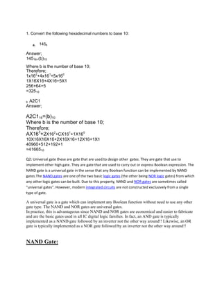
  • 1. 1. Convert the following hexadecimal numbers to base 10: a. 1458 Answer; 14516=(b)10 Where b is the number of base 10; Therefore; 1x162+4x161+5x160 1X16X16+4X16+5X1 256+64+5 =32510 b .A2C1 Answer; A2C116=(b)10 Where b is the number of base 10; Therefore; AX163+2X162+CX161+1X160 10X16X16X16+2X16X16+12X16+1X1 40960+512+192+1 =4166510 Q2: Universal gate these are gate that are used to design other gates. They are gate that use to implement other high gate. They are gate that are used to carry out or express Boolean expression. The NAND gate is a universal gate in the sense that any Boolean function can be implemented by NAND gates.The NAND gates are one of the two basic logic gates (the other being NOR logic gates) from which any other logic gates can be built. Due to this property, NAND and NOR gates are sometimes called "universal gates". However, modern integrated circuits are not constructed exclusively from a single type of gate. A universal gate is a gate which can implement any Boolean function without need to use any other gate type. The NAND and NOR gates are universal gates. In practice, this is advantageous since NAND and NOR gates are economical and easier to fabricate and are the basic gates used in all IC digital logic families. In fact, an AND gate is typically implemented as a NAND gate followed by an inverter not the other way around!! Likewise, an OR gate is typically implemented as a NOR gate followed by an inverter not the other way around!! NAND Gate:
  • 2. The NAND gate represents the complement of the AND operation. Its name is an abbreviation of NOT AND. The graphic symbol for the NAND gate consists of an AND symbol with a bubble on the output, denoting that a complement operation is performed on the output of the AND gate. The truth table and the graphic symbol of NAND gate is shown below; NAND Gate is a Universal Gate; To prove that any Boolean function can be implemented using only NAND gates, we will show that the AND, OR, and NOT operations can be performed using only these gates. Implementing an Inverter Using only NAND Gate; 1. All NAND input pins connect to the input signal Agives an output A’. 2. One NAND input pin is connected to the input signal A while all other input pins are connected to logic 1. The output will be A’.
  • 3. Implementing an AND using only NAND GATE; 3. An AND gate can be replaced by NAND with its output complemented by a NAND gate inverter. Implementing OR Using only NAND Gates; 4. An OR gate can be replaced by NAND with it’s input complemented by a NAND gate inverter. Thus ,the NAND gate is a unversal gate since it can implement the AND,OR and NOT functions.
  • 4. NOR Gate: The NOR gate represents the complement of the OR operation. Its name is an abbreviation of NOT OR. The graphic symbol for the NOR gate consists of an OR symbol with a bubble on the output, denoting that a complement operation is performed on the output of the OR gate. The truth table and the graphic symbol of NOR gate as show below; The truth table clearly shows that the NOR operation is the complement of the OR. NOR Gate is a Universal Gate: To prove that any Boolean function can be implemented using only NOR gates, we will show that the AND, OR, and NOT operations can be performed using only these gates. Implementing and inverter using NOR gate; 1. All NOR input pins connect to the input signal A gives an output A’. 2. One NOR input pin is connected to the input signal A while all other input pins are connected to logic 0. The output will be A’.
  • 5. Implementing OR Using only NOR Gates; 1. The OR is replaced by a NOR gate with it's output complemented by a NOR gate inverter. Implementing AND Using only NOR Gates; 2. The NAND gates is replaced by a NOR gate with all it's inputs complemented by NOR gates inverters. 1 Thus, the NOR gate is a universal gate since it can implement the AND, OR and NOT functions. The reason why they are called universal gate; 1. Universal gates are the ones from which we can design other gates also. foreg. NAND and NOR gates. they help in forming the uniformity in the circuits. 2. NAND and NOR both are called as universal gate. You can built any circuit or design using either NAND or NOR, this will be so flexible to fabricate any circuit in a single chip 3. They are less expensive to construct 5. Draw and explain the working of JK, S-R, and D flip flops. JK flip-flop
  • 6. A circuit symbol for a positive-edge-triggered JK flip-flop JK flip-flop timing diagram The JK flip-flop augments the behavior of the SR flip-flop (J=Set, K=Reset) by interpreting the S = R = 1 condition as a "flip" or toggle command. Specifically, the combination J = 1, K = 0 is a command to set the flip-flop; the combination J = 0, K = 1 is a command to reset the flip-flop; and the combination J = K = 1 is a command to toggle the flip-flop, i.e., change its output to the logical complement of its current value. Setting J = K = 0 does NOT result in a D flip-flop, but rather, will hold the current state. To synthesize a D flip-flop, simply set K equal to the complement of J. Similarly, to synthesize a T flip-flop, set K equal to J. The JK flip-flop is therefore a universal flip-flop, because it can be configured to work as an SR flip-flop, a D flip- flop, or a T flip-flop. The characteristic equation of the JK flip-flop is: and the corresponding truth table is: JK Flip Flop operation[28] Characteristic table Excitation table J K Qnext Comment Q Qnext J K Comment 0 0 Q hold state 0 0 0 X No change 0 1 0 reset 0 1 1X Set 1 0 1 set 1 0 X 1 Reset 1 1 Q toggle 1 1 X 0 No change
  • 7. S-R NOR latch An SR latch, constructed from a pair of cross-coupled NOR gate (an animated picture). Red and black mean logical '1' and '0', respectively. When using static gates as building blocks, the most fundamental latch is the simple S-R latch, where S and R stand for set and reset. It can be constructed from a pair of cross-coupled NORlogic gates. The stored bit is present on the output marked Q. While the S and R inputs are both low, feedback maintains the Q and Q outputs in a constant state, with Q the complement of Q. If S (Set) is pulsed high while R (Reset) is held low, then the Q output is forced high, and stays high when S returns to low; similarly, if R is pulsed high while S is held low, then the Q output is forced low, and stays low when R returns to low. S-R Flip Flop operation Characteristic table Excitation table S R Qnext Action Q Qnext S R 00 Q hold state 0 0 0 x 01 0 reset 0 1 1 0 10 1 set 1 0 0 1 1 1 X not allowed 1 1 X 0 The R = S = 1 combination is called a restricted combination or a forbidden state because, as both NOR gates then output zeros, it breaks the logical equation Q = not Q. The combination is also inappropriate in circuits where both inputs may go low simultaneously (i.e. a transition from restricted to keep). The output would lock at either 1 or 0 depending on the propagation time relations between the gates (a race condition). In certain implementations, it could also lead to
  • 8. longer ringings (damped oscillations) before the output settles, and thereby result in undetermined values (errors) in high-frequency digital circuits. Although this condition is usually avoided, it can be useful in some applications. To overcome the restricted combination, one can add gates to the inputs that would convert (S,R) = (1,1) to one of the non-restricted combinations. That can be: Q = 1 (1,0) – referred to as an S-latch Q = 0 (0,1) – referred to as an R-latch Keep state (0,0) – referred to as an E-latch Alternatively, the restricted combination can be made to toggle the output. The result is the JK latch. Characteristic: Q+ = R'Q + R'S or Q+ = R'Q + S Gated SR latch A gated SR latch circuit diagram constructed from NOR gates. A synchronous SR latch (sometimes clocked SR flip-flop) can be made by adding a second level of NAND gates to the inverted SR latch (or a second level of AND gates to the direct SR latch). The extra gates further invert the inputs so the simple SR latch becomes a gated SR latch (and a simple SR latch would transform into a gated SR latch with inverted enable). With E high (enable true), the signals can pass through the input gates to the encapsulated latch; all signal combinations except for (0,0) = hold then immediately reproduce on the (Q,Q) output, i.e. the latch is transparent. With E low (enable false) the latch is closed (opaque) and remains in the state it was left the last time E was high. The enable input is sometimes a clock signal, but more often a read or write strobe.
  • 9. Gated S-R latch operation E/C Action 0 No action (keep state) Symbol for a gated SR latch 1 The same as non-clocked SR latch Gated D latch A D-type transparent latch based on an SR NAND latch A gated D latch based on an SR NOR latch This latch exploits the fact that, in the two active input combinations (01 and 10) of a gated SR latch, R is the complement of S. The input NAND stage converts the two D input states (0 and 1) to these two input combinations for the next SR latch by inverting the data input signal. The low state of the enable signal produces the inactive "11" combination. Thus a gated D-latch may be considered as a one-input synchronous SR latch. This configuration prevents application of the restricted input combination. It is also known as transparent latch, data latch, or simply gated latch. It has a data input and an enable signal (sometimes named clock, or control). The word transparent comes from the fact that, when the enable input is on, the signal propagates directly through the circuit, from the input D to the output Q.
  • 10. Transparent latches are typically used as I/O ports or in asynchronous systems, or in synchronous two-phase systems (synchronous systems that use a two-phase clock), where two latches operating on different clock phases prevent data transparency as in a master–slave flip-flop. Latches are available as integrated circuits, usually with multiple latches per chip. For example, 74HC75 is a quadruple transparent latch in the 7400 series. Gated D latch truth table E/C D Q Q Comment 0 X Qprev Qprev No change 1 0 0 1 Reset Symbol for a gated D latch 1 1 1 0 Set The truth table shows that when the enable/clock input is 0, the D input has no effect on the output. When E/C is high, the output equals D. D flip-flop D flip-flop symbol The D flip-flop is widely used. It is also known as a data or delay flip-flop. The D flip-flop captures the value of the D-input at a definite portion of the clock cycle (such as the rising edge of the clock). That captured value becomes the Q output. At other times, the output Q does not change. The D flip-flop can be viewed as a memory cell, a zero-order hold, or a delay line.
  • 11. Truth table: Clock D Qnext Rising edge 0 0 Rising edge 1 1 Non-Rising X Q ('X' denotes a Don't care condition, meaning the signal is irrelevant) Most D-type flip-flops in ICs have the capability to be forced to the set or reset state (which ignores the D and clock inputs), much like an S-R flip-flop. Usually, the illegal S = R = 1 condition is resolved in D-type flip-flops. By setting S = R = 0, the flip-flop can be used as described above. Inputs Outputs S R D > Q Q' 0 1 X X 0 1 1 0 X X 1 0 1 1 X X 1 1 4-bit serial-in, parallel-out (SIPO) shift register
  • 12. These flip-flops are very useful, as they form the basis for shift registers, which are an essential part of many electronic devices. The advantage of the D flip-flop over the D-type "transparent latch" is that the signal on the D input pin is captured the moment the flip-flop is clocked, and subsequent changes on the D input will be ignored until the next clock event. An exception is that some flip-flops have a "reset" signal input, which will reset Q (to zero), and may be either asynchronous or synchronous with the clock. The above circuit shifts the contents of the register to the right, one bit position on each active transition of the clock. The input X is shifted into the leftmost bit position. Classical positive-edge-triggered D flip-flop A positive-edge-triggered D flip-flop This clever circuit consists of two stages implemented by S-R NAND latches. The input stage (the two latches on the left) processes the clock and data signals to ensure correct input signals for the output stage (the single latch on the right). If the clock is low, both the output signals of the input stage are high regardless of the data input; the output latch is unaffected and it stores the previous state. When the clock signal changes from low to high, only one of the output voltages (depending on the data signal) goes low and sets/resets the output latch: if D = 0, the lower output becomes low; if D = 1, the upper output becomes low. If the clock signal continues staying high, the outputs keep their states regardless of the data input and force the output latch to stay in the corresponding state as the input logical zero remains active while the clock is high. Hence the role of the output latch is to store the data only while the clock is low. The circuit is closely related to the gated D latch as both the circuits convert the two D input states (0 and 1) to two input combinations (01 and 10) for the output S-R latch by inverting the data input signal (both the circuits split the single D signal in two complementary S and R signals). The difference is that in the gated D latch simple NAND logical gates are used while in the positive-edge-triggered D flip-flop SR NAND latches are used for this purpose. The role of these latches is to "lock" the active output producing low voltage (a logical zero); thus the positive-edge-triggered D flip-flop can be thought of as a gated D latch with latched input gates.
  • 13. Q6. Give any two applications of a shift register. Answer 1. Very effective for sequence detectors. 2. Shift register are often used as the state register in a sequential device. Q7. Explain the working principle of a 4 bit Johnson counter with a neat diagram. Answer. The demonstration above initially implements only the legitimate counting sequence of the Johnson counter. To allow for all possible illegal combinations and show how they get straightened out, we
  • 14. would need 66 separate images for the over lays, and each is about 6.5k bytes in size. That’s a bit much to ask of many users. however, you can see the count correction gates operating at the bottom of the counter, and see how they work. The D input to flip-flop C is not directly driven from the B output. Rather , A’ and C’ are added together, and that combination is NO Red with B’, as a result, improper bits reaching flip-flop B get blocked, and flip-flop C can only take on the correct state to reinstate the correct shifting sequence. To see this in action, you can click on any of the individual flip-flops in the figure. This will force a load of all remaining images and change the state of the selected flip-flop without applying a clock pulse. Then you can watch the behavior of the counter as it removes improper counting sequences. Remember that the download of the additional images may take some time, so please be patient. You can only identify an illegal counting sequence because more than one output will be high (logic 1). Since each output is enabled by a transition from 0 to 1 or from 1 to 0 in a specific position in the counter, more than one transition will produce more than one output, which is illegal in this context. Also note that in order to repeatedly invert the shifting bits as they start from flip-flop A, the E' output is fed back to the A flip-flop's D input. This shift does not constitute a second transition here; only when all bits are the same does this appear as a transition. Of course, these must necessarily be edge-triggered flip-flops clocked simultaneously. The Reset inputs are asynchronous and override the clocking signal. In addition, the CMOS ICs that serve as the model for this demonstration change state on the rising edge of the clock, so this model does the same. The COUT signal is the Carry Out, which is a symmetrical square wave at one-tenth of the incoming Clock signal frequency. It is quite suitable for clocking a second counter of the same type, to form a multiple-digit decimal counter. Q8. Explain temperature and weather forecast system with a neat circuit diagram. Answer;
  • 15. Hardware calibration is simply a matter of setting the offset voltage to the value listed in table 1 for your altitude. A jumper on the input of the DS2438 allows the use of the DS2438 to measure the offset. Put the jumper in the A-C position and using the iButton Viewer for the DS2438, set the voltage to the table value using the 25-turn pot. Once it’s set, put the jumper in the A-B position to read pressure. For altitudes in between the values listed in the table, simple interpolation will give accurate results. An Excel spreadsheet will be also available online to calculate intermediate values. Software: Routines currently exist to measure the DS2438s Vad voltage. Once this voltage is measured, the pressure is calculated using: Press = slope * Vad + intercept Where the slope and intercept are the values listed in table 1 for your altitude. The prototype code I used had an external text file to store the slope and intercept values. This allows the user to edit the file to fine-tune the calibration if desired.
  • 16. Fine-tuning can be accomplished by monitoring the pressure and comparing it with a known reference source, such as a nearby airport or NOAA weather. Start by adjusting the intercept. When the reference station indicates a pressure near mid-scale (30.00 inHg), adjust the software intercept value until your weather station matches. Now monitor the pressure extremes to determine if the slope needs adjustment. An Excel spreadsheet will be available as an aid. Q10. Write a short note on ADC. Answer; ADC An analog-to-digital converter (abbreviated ADC, A/D or A to D) is an electronic integrated circuit, which converts continuous signals to discrete digital numbers. Typically, an ADC is an electronic device that converts an input analog voltage (or current) to a digital number. The digital output may be using different coding schemes, such as binary, Gray code or two's complement binary. However, some non-electronic or only partially electronic devices, such as rotary encoders, can also be considered ADCs. Working Principle & Circuits of Analog to Digital Concepts Resolution The resolution of the converter indicates the number of discrete values it can produce over the range of analog values. The values are usually stored electronically in binary form, so the resolution is usually expressed in bits. In consequence, the number of discrete values available, or "levels", is usually a power of two. For example, an ADC with a resolution of 8 bits can encode an analog input to one in 256 different levels, since 28 = 256. The values can represent the ranges from 0 to 255 (i.e. unsigned integer) or from -128 to 127 (i.e. signed integer), depending on the application. Resolution can also be defined electrically, and expressed in volts. The voltage resolution of an ADC is equal to its overall voltage measurement range divided by the number of discrete intervals as in the formula: Where: Q is resolution in volts per step (volts per output code), N E 2 E Q FSR M FSR EFSR is the full scale voltage range = VRefHi − VRefLo and M is the ADC's resolution in bits. The number of intervals is given by the number of available levels (output codes), which is: N = 2M Some examples may help:
  • 17. Example: Full scale measurement range = 0 to 10 volts ADC resolution is 12 bits: 212 = 4096 quantization levels (codes) ADC voltage resolution is: (10V - 0V) / 4096 codes = 10V / 4096 codes 0.00244 volts/code 2.44 mV/code Response type Linear ADCs Most ADCs are of a type known as linear, although analog-to-digital conversion is an inherently non- linear process (since the mapping of a continuous space to a discrete space is a piecewise-constant and therefore non-linear operation). The term linear as used here means that the range of the input values that map to each output value has a linear relationship with the output value, i.e., that the output value k is used for the range of input values from m(k + b) to m(k + 1 + b), where m and b are constants. Here b is typically 0 or −0.5. When b = 0, the ADC is referred to as mid-rise, and when b = −0.5 it is referred to as mid-tread. Non-linear ADCs If the probability density function of a signal being digitized is uniform, then the signal-to-noise ratio relative to the quantization noise is the best possible. Because of this, it's usual to pass the signal through its cumulative distribution function (CDF) before the quantization. This is good because the regions that are more important get quantized with a better resolution. In the dequantization process, the inverse CDF is needed. This is the same principle behind the commanders used in some tape- recorders and other communication systems, and is related to entropy maximization. (Never confuse commanders with compressors!) For example, a voice signal has a Laplacian distribution. This means that the region around the lowest levels, near 0, carries more information than the regions with higher amplitudes. Because of this, logarithmic ADCs are very common in voice communication systems to increase the dynamic range of the represent able values while retaining fine-granular fidelity in the low- amplitude region Accuracy An ADC has several sources of errors. Quantization error and (assuming the ADC is intended to be linear) non-linearity is intrinsic to any analog-to-digital conversion. There is also a so-called aperture error which is due to a clock jitter and is revealed when digitizing a time-variant signal (not a constant value). These errors are measured in a unit called the LSB, which is an abbreviation for least significant bit. In the above example of an eight-bit ADC, an error of one LSB is 1/256 of the full signal range, or about 0.4%. Quantization error Quantization error is due to the finite resolution of the ADC, and is an unavoidable imperfection in all types of ADC. The magnitude of the quantization error at the sampling instant is between zero and half of one LSB. In the general case, the original signal is much larger than one LSB. When this happens, the quantization error is not correlated with the signal, and has a uniform distribution. Its RMS value is the standard deviation of this distribution, given by In the eight-bit ADC example, this represents 0.113% of the full signal range. At lower levels the quantizing error becomes dependent of the input signal, resulting in distortion. This distortion is created after the anti-aliasing filter.
  • 18. Sampling rate The analog signal is continuous in time and it is necessary to convert this to a flow of digital values. It is therefore required to define the rate at which new digital values are sampled from the analog signal. The rate of new values is called the sampling rate or sampling frequency of the converter. A continuously varying band limited signal can be sampled (that is, the signal values at intervals of time T, the sampling time, are measured and stored) and then the original signal can be exactly reproduced from the discrete- time values by an interpolation formula. The accuracy is limited by quantization error. However, this faithful reproduction is only possible if the sampling rate is higher than twice the highest frequency of the signal. This is essentially what is embodied in the Shannon-Nyquist sampling theorem. Since a practical ADC cannot make an instantaneous conversion, the input value must necessarily be held constant during the time that the converter performs a conversion (called the conversion time). An input circuit called a sample and hold performs this task – in most cases by using a capacitor to store the analogue voltage at the input, and using an electronic switch or gate to disconnect the capacitor from the input. Many ADC integrated circuits include the sample and hold subsystem internally. Aliasing All ADCs work by sampling their input at discrete intervals of time. Their output is therefore an incomplete picture of the behavior of the input. There is no way of knowing, by looking at the output, what the input was doing between one sampling instant and the next. If the input is known to be changing slowly compared to the sampling rate, then it can be assumed that the value of the signal between two sample instants was somewhere between the two sampled values. If, however, the input signal is changing fast compared to the sample rate, then this assumption is not valid. If the digital values produced by the ADC are, at some later stage in the system, converted back to analog values by a digital to analog converter or DAC, it is desirable that the output of the DAC be a faithful representation of the original signal. If the input signal is changing much faster than the sample rate, then this will not be the case, and spurious signals called aliases will be produced at the output of the DAC. The frequency of the aliased signal is the difference between the signal frequency and the sampling rate. For example, a 2 kHz sine wave being sampled at 1.5 kHz would be reconstructed as a 500 Hz sine wave. This problem is called aliasing. To avoid aliasing, the input to an ADC must be low-pass filtered to remove frequencies above half the sampling rate. This filter is called an anti-aliasing filter, and is essential for a practical ADC system that is applied to analog signals with higher frequency content. Although aliasing in most systems is unwanted, it should also be noted that it can be exploited to provide simultaneous down-mixing of a band-limited high frequency signal (see frequency mixer). Dither In A to D converters, performance can usually be improved using dither. This is a very small amount of random noise (white noise) which is added to the input before conversion. Its amplitude is set to be about half of the least significant bit. Its effect is to cause the state of the LSB to randomly oscillate between 0 and 1 in the presence of very low levels of input, rather than sticking at a fixed value. Rather than the signal simply getting cut off altogether at this low level (which is only being quantized to a resolution of 1 bit), it extends the effective range of signals that the A to D converter can convert, at the expense of a slight increase in noise - effectively the quantization error is diffused across a series of noise
  • 19. values which is far less objectionable than a hard cutoff. The result is an accurate representation of the signal over time. A suitable filter at the output of the system can thus recover this small signal variation An audio signal of very low level (with respect to the bit depth of the ADC) sampled without dither sounds extremely distorted and unpleasant. Without dither the low level always yields a '1' from the A to D. With dithering, the true level of the audio is still recorded as a series of values over time, rather than a series of separate bits at one instant in time. A virtually identical process, also called dither or dithering, is often used when quantizing photographic images to a fewer number of bits per pixel –the image becomes noisier but to the eye looks far more realistic than the quantized image, which otherwise becomes banded. This analogous process may help to visualize the effect of dither on an analogue audio signal that is converted to digital. Dithering is also used in integrating systems such as electricity meters. Since the values are added together, the dithering produces results that are more exact than the LSB of the analog- to-digital converter. Note that dither can only increase the resolution of a sampler, it cannot improve the linearity, and thus accuracy does not necessarily improve. been used. With this technique, it is possible to obtain an effective resolution larger than that provided by the converter alone. ADC structures These are the most common ways of implementing an electronic ADC: A direct conversion ADC or flash ADC has a bank of comparators, each firing for their decoded voltage range. The comparator bank feeds a logic circuit that generates a code for each voltage range. Direct conversion is very fast, but usually has only 8 bits of resolution (255 comparators - since the number of comparators required is 2n - 1) or fewer, as it needs a large, expensive circuit. ADCs of this type have a large die size, a high input capacitance, and are prone to produce glitches on the output (by outputting an out-of- sequence code). Scaling to newer submicron technologies does not help as the device mismatch is the dominant design limitation. They are often used for video, wideband communications or other fast signals in optical storage. A successive-approximation ADC uses a comparator to reject ranges of voltages, eventually settling on a final voltage range. Successive approximation works by constantly comparing the input voltage to the output of an internal digital to analog converter (DAC, fed by the current value of the approximation) until the best approximation is achieved. At each step in this process, a binary value of the approximation is stored in a successive approximation register (SAR). The SAR uses a reference voltage (which is the largest signal the ADC is to convert) for comparisons. For example if the input voltage is 60 V and the reference voltage is 100 V, in the 1st clock cycle, 60 V is compared to 50 V (the reference, divided by two. This is the voltage at the output of the internal DAC when the input is a '1' followed by zeros), and the voltage from the comparator is positive (or '1') (because 60 V is greater than 50 V).