8051 Programming Instruction Set
•Télécharger en tant que PPT, PDF•
13 j'aime•7,496 vues

Introduction to the 8051 instruction set

Recommandé
Contenu connexe
Tendances
Tendances (20)
Similaire à 8051 Programming Instruction Set
Similaire à 8051 Programming Instruction Set (20)
Plus de Shreyans Pathak
Dernier
Dernier (20)
8051 Programming Instruction Set
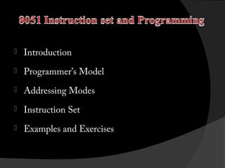
- 1. Introduction Programmer’s Model Addressing Modes Instruction Set Examples and Exercises
- 2. Valve Analog sensor Analog Mux DAC ADC Interrupt Stepper motor Timer Counter Digital sensor Digital Mux µp Digital Actuator D mux Alarm Annunciator Binary Switches Digital Mux Memory I/O System
- 3. SUB SYSTEMS - ANALOG SENSORS - DIGITAL SENSORS -BINARY SWITCHES µP + Memory + I/O D MUX - DAC + Valve - Stepper Motor -Digital Actuator - Alarm Annunciator MUX
- 4. General Facilities 8 bit CPU On chip clock oscillator 4 KB of ROM (Program memory) 128 bytes RAM (Data Memory) 21 Special Function Registers(SFR) 32 I/O lines (Ports P0 to P3) 64 KB address space for external data memory 64 KB address space for program memory 2- 16 bit timer/counter 5 source interrupt structure
- 5. Full duplex serial port Bit addressability Bit processing capability MCS-51 compatible chips 8031 – Romless version – 4KB ROM not available 8751 – EPROM version – 4KB EPROM 8052- (8 KB ROM + 256 byte Data memory)
- 7. Resources used in programming Memory Special Function Register Program status word Memory – Program Memory - 4 KB on chip ROM 60 KB External RAM or 64 KB External RAM 64 KB Internal Data memory – 256 bytes 128 bytes Internal Data RAM 21 SFRS
- 8. 0FFF 0000
- 9. Internal Data memory - 128 bytes internal data RAM is divided into 32 bytes - 4 banks of Register R0-R7. - 00-1FH Register Bank selected by using 2 bits RS0 & RSI in PSW. - 20 – 2FH 30 – 7FH 16 bytes direct addressing bits (total 128 bit addresses). 80 bytes general purpose RAM.
- 11. 80- FFH
- 14. Memory Map of 8051 FFFF FFFF External (60 KB) 1000 Over lapped Space 0FFF 0FFF Internal (EA = 1) (4 KB) 0000 64 KB FF External (EA = 0) (4 KB) 0000 Program Memory 80 7F SFRs Internal Data RAM 0000 00 Internal Data Memory External Data Memory
- 15. 7 FH 48 80 bytes 127 30 H 2 FH 127(7F) ----------------------------120(78 H) 16 bytes 32 7 24 16 32 bytes 8 00 0 Reg. Bank 3 Reg. Bank 2 Reg. Bank 1 20 H 1 FH 18 H 17 H 10 H 0FH 00H 07H Reg. Bank 0 00H Internal Data RAM Byte Addressing – General Purpose Direct Addressable bits
- 16. 7 Cr 6 AC 5 4 3 RS1 2 RS0 User Flag 0 0 P Reserved bit CY- (PSW-7)- Set if operation results in carry out of (during addition) or a borrow in to (during subtraction) the higher order bit of the result otherwise CY in reset. Carry 1 OV 0F FH + 1 = 1 1 1 1 10000 1111 +1 0000 02H – 5 = 0000 0010 10 1 Borrow 11 1 1 1 1101
- 17. AC- (PSW.6) - is set if operation results in carry out of Lower Nibble (during addition) to Higher Nibble or borrow from Higher Nibble to Lower Nibble (during subtraction) otherwise it is cleared. ( Used For BCD addition/Subtraction) RS1 , RS0 (PSW.4, PSW.3) - represent the current register bank in the internal data RAM selected. PSW SFR is bit addressable. RS1 RS0 0 0 - Bank 0 0 1 - Bank 1 1 0 - Bank 2 1 1 - Bank 3 Default - Bank 0 OV – Overflow (PSW.2) is set if operation results in carry in to the higher order bit of result but not carry out of higher order bit or vice versa. OV has significant role in two’s compliment arithmetic, since it becomes set when signed result can’t be represented in 8 bits.
- 18. Example (1) - 0 111 1111 + 0 000 0001 1 000 0000 Carry in to MSB but not out of MSB Example (2) = +127 OV set Result = -ve no. - 1 + -1 = -2 -1 = 1 1 1 1 - 1 = 1 111 1111 1 1110 Carry CY is set 111 Carry 1111 OV in not set Sign of result is correct. If you consider CY is 8th bit then the result is -2 only. CY 1 1111 1110 1’s compliment = 0 0000 0001 +1 = 0 0000 0010
- 19. P-odd parity (PSW.0) – is set if no. of ones in the accumulator is odd otherwise it is cleared (even parity). User flag 0 and Reserved bit are for internal use of chip. Not available to programmer.
- 20. Bytes - Unsigned 8 bit nos. , ASCII code etc Short Integer – Signed number. Bits – are represented in Bit addressable RAM. - 128 bits within internal data RAM. - 128 bits within SFR may be addressed directly. Separate instructions for bit processing. CY is used in bit processing as ACC. 16 bit operations are not facilitated. Thus 16 bit operand can’t be addressed. In MUL instruction (Multiplication) MUL AB Operand 1 Stored in ACC. Operand 2 Stored in B reg. Result in 16 bits stored in B reg. (higher bytes) and ACC (lower bytes).
- 21. In Div instruction (DIV) DIV AB Operand1 - Stored in ACC (8 bits) Operand 2 – Stored in B register (8 bits) A/B is performed Result – Quotient – Stored in ACC Remainder – Stored in B register
- 22. Immediate Addressing Register Addressing Direct Addressing Register indirect Addressing Base Register plus index register indirect addressing.
- 23. Operand on which operation to be performed is part of instruction. Example: - MOV Rn, # data (n = 0 to 7) (Rn) data - ADD A , # data (A) (A) + data - ADD A , # 0FH
- 24. Example:ADD A, # 0FH : 0FH ADD A + 1FH Program Memory : 10 H E0H (ACC) | | | | | Internal Data Memory Bank1 Reg. Bank R1 R0
- 25. Register R0 – R7, A, B, DPTR and SFR register may be accessed. Reg. bank may be selected by RS1 RS0 bits of PSW. Example – MOV A , R2 (A) (R2) Program MOV A , R2 ADD A , R3 Memory (A) (A) + (R3) DEC R2 (R2) (R2) - 1 E0H ACC 24 H 02 01 00 24 H R2 R1 R0
- 26. Address of operand is specified in the instruction. - may be byte operand or bit operand. • Direct Addressing of byte operand may be. - Lower 128 byte of Internal Data RAM i.e Address 00 to 7FH - Special Function Register. Direct bit address provides operation on - 128 bit subset of Internal Data RAM (20H to 2FH) - Subsets of SFR address space (80H to FFH) Out of 21 SFR’s , 11 SFRS are direct bit addressable. Note – Only Internal data RAM space can be directly addressed.
- 27. Example – X EQU 48 H MOV A, X MOV X, # 30H ADD A, X (A) (X) (A) (X) (48 H) (30H) (A)+ (X) Program Memory H 87 E0H A + 48 H
- 29. Example – MOV A, @ R0 (R0 has the address of operand) (A) ((R0)) A E0H 33H 2 52 H 1 R0 00
- 30. For external data RAM , 16 bit register DPTR may be used to access any location within full 64 KB memory R0 and R1 may be used for up to 0FFH external data memory space. Instruction is MOVX Example - MOVX A, @ R1 (A) ((R1)) MOV DPTR, # 0240FH MOVX @ DPTR , A MOVX A, @ DPTR (( DPTR)) (A) (A) ((DPTR))
- 32. Used to access program memory. Operand is not specified directly. Operand Address = (Base Reg) + (Index reg.) Base Register – DPTR or PC – 16 bit register Index Reg – ACC Thus Operand Address = (A) + (DPTR) or (A) + (PC) as specified in the instruction. Instruction is MOVC C – means program memory access Example- MOVC A, @ A+DPTR (A) ((A) + (DPTR) Used for reading already stored arrays as part of program memory
- 33. Example:ARRAY : DB 3FH, 39H, 0FH, 37H ----MOV R5, #0AH MOV DPTR, #ARRAY MOV A, #00H KK1 : MOVC A, @ A + DPTR ------------------------------INC A DJNZ R5 , KK1
- 34. MOVC A, @ A + DPTR 0502 0FH 0501 Program Memory 39H 0500 3FH 3 2 A 00 E0H 1 + 0500H 1 DPTR DPH DPL 05 00 83H 82H
- 35. General Purpose Data Transfer Accumulator Specific Data Transfer Address Object Data Transfer
- 36. . MOV – byte or bit transfer . PUSH - byte to stack . POP - byte from stack (Flags not effected unless PSW in being modified)
- 37. MOV Rn, # data – Immediate Addressing MOV A, # data - Immediate Addressing MOV Rn, A - Register Addressing Note - MOV Ri , Rj – Not allowed MOV A, Rn – Register Addressing MOV A, Direct – Direct Addressing MOV Direct , A - Direct Addressing MOV Direct , Rn - Direct Addressing MOV Rn , Direct - Direct Addressing MOV Direct , Direct - Direct Addressing
- 38. MOV @Ri , A – Indirect Addressing MOV A , @Ri -Indirect Addressing MOV Direct, @Ri – Direct + Indirect MOV @Ri, Direct – Direct + Indirect (Ri = Ro or R1) MOV Direct, # Data - Direct + immediate MOV @ Ri , # Data – Indirect + immediate
- 39. MOV < dest. bit> <Src. bit> Move bit variable. Carry acts as ACC for bit operation . MOV C , bit (C) (bit) MOV bit , C PUSH Direct (SP) ((SP)) (SP) + 1 (Direct) POP Direct (Direct) (SP) ((SP)) (SP) - 1
- 40. XCH – Exchange data between A reg. and byte source operand XCHD –Exchange lower Nibble in A with Lower Nibble of source operand (Indirect Addressing). MOVX – Data transfer between external data memory and A register(Indirect Addressing). External address in DPTR. MOVC – Move byte from program memory to A. (Base Reg + Index reg. indirect addressing) XCH A, <byte> XCH A, Rn – Register Addressing XCH A, direct – Direct Addressing XCH A, @Ri – Indirect Addressing
- 41. XCHD A, @Ri (Ri = R0 or R1) MOVX < dest. Byte> <src. Byte> MOVX A, @ Ri MOVX A , @ DPTR MOVX @ Ri, A MOVX @ DPTR , A MOVC A, @A + DPTR (Move code byte) (A) ((DPTR)+(A)) MOVC A, @A + PC (A) (( PC) +(A))
- 42. Address object Transfer Move 16 bit address as immediate data to DPTR MOV DPTR, # Data16
- 43. Flags are affected Operations – Add , Subtract , Multiply, Divide, Increment, Decrement. Only 8 bit operations are permitted. ADDITION:ADD A, (src. Byte) - Add (A) (A) + (Src.) ADDC A, (Src byte) Add with carry (A) (A) +(Src) + (C) Register AddressingADD A, Rn (A) (A)+(Rn) ADDC A, Rn (A) (A)+(Rn)+(C)
- 44. Direct Addressing src = direct address (A) (A)+(direct)+(C) (A) (A) + (direct) Indirect Addressing src = @Ri (R1 or R2) (A) (A)+((Ri)) (A) (A) + ((Ri)) + (C) Immediate Addressing src = # data (A) (A) + data (A) (A)+(C)+data INCREMENT INC <byte> INC A, INC Rn , INC @Ri, INC direct INC DPTR is additional instruction (DPTR) (DPTR) + 1
- 45. SUBTRACTION SUBB , DEC Decrement Subtract with Borrow SUBB A, <Src. byte)> (A) (A) - (Src) (C) Register –Src = Rn Indirect – Src = @Ri ( i =0 or 1) Direct – Src = direct Immediate- Src = # data SUBB A, @Ri – (A) DEC <byte> (A)-((Ri)) – (C) <byte> = A, Rn ,@ Ri ,direct DEC A , DEC Rn , DEC @ Ri , DEC direct
- 46. MULTIPLY MUL AB (A) - Operand 1, (B) – (Operand 2) After operation (A) - lower order byte of Result (B) - Higher order byte DIVIDE DIV AB (A)/(B) quotient in A remainder in B
- 47. DA A (Decimal Adjust Accumulator for addition) If two BCD numbers (in packed BCD format) are added using ADD or ADDC instructions then to represent the result in BCD. DA A instruction is used, Algorithms is(1) If value of lower Nibble in ACC > 9 or if AC Flag is set then 6 is added to ACC. (2) Now after (1), if value of higher Nibble is greater than 9 or if CY Flag is set then 6 is added to higher Nibble of ACC.
- 48. Example :A & R3 have BCD number 6 8 A= R3 = 0110 1000 A= R3= 2 4 0010 0100 After ADD A, R3 instruction. 1100 A = 1000 Not in BCD DA A instruction (1) Lower Nibble = 12 i.e > 9 (A) (A) + 6 + 0110 = 1001 1000 1100 0010 (2) Higher Nibble = 9 , CY=0 So no action – Result 92 is BCD number.
- 50. 1 7 7 CY 6 0 1 0
- 51. RR A Rotate ACC Right 7 RRC A 6 1 0 Rotate ACC Right through Carry 7 6 1 0 CY SWAP A (Swap Nibble in ACC) 7 6 5 4 3 2 1 Basically RR A or RL A four times. 0
- 53. XOR XRL A, <Src> (A) (A) V (Src) Register addressing – Src =Rn , Direct addressing – Src = direct Immediate addressing– Src = #data , Indirect addressing – Src = @Ri Two more Instructions XRL direct , A (direct) XRL direct, # data (direct) (direct) V (A) (direct) V data
- 54. - Unconditional calls, Returns and jumps - Conditional Jumps - Interrupts
- 55. ACALL addr.11 (Absolute Call) CALL to subroutine located within 2kb memory block
- 56. Main program ACALL ------------------------Subroutine FACT: ----------------RET 1 FACT 2 KB 2 (1) Program counter is saved in the stack. Address of Subroutine is loaded to PC. (2) Program counter value is retrieved from stack.
- 57. LCALL addr. 16 (Long call) Call can be made to full 64KB space. LCALL FACT ----------------------FACT: ---------------------RET
- 58. AJMP addr 11 (Absolute Jump) Jump to instruction in 2KB block LJMP addr16 (Long Jump) Jump can be any where in memory space SJMP rel (Short Jump) Jump can be 128 bytes before or 127 bytes after the instruction
- 59. AJMP CALC ------------------CALC: ------------KALC: 128 LJMP CALC --------------------CALC: --------------- 2 KB bytes SJMP KALC --------------- Either of them 127 bytes KALC: --------------- No limit
- 60. JMP @A + DPTR (PC) (A)+ (DPTR) For case statements. Return from Interrupt – RETI No operation - NOP
- 61. Condition - bit set or bit not set - result in ACC is zero or not zero - rel. Jump to 128 byte before 127 after JB bit, rel. (Jump if bit set) JB P0.3 , NEXT NEXT:
- 62. JNB JC bit, rel (Jump if bit not set) rel (Jump if carry set) JNC rel (Jump if carry not set) JBC bit, rel (Jump if bit is set and clear bit) JZ rel , Jump if result in ACC is zero JNZ rel , Jump if result in ACC is not zero.
- 63. CJNE <dest>, <Src>,rel. If (dest) # (Src) then jump to specified address. If <dest> less than <Src> CY=1 If <dest> greater than <src> CY =0 CJNE A, direct, rel CJNE A, #data, rel CJNE Rn, #data, rel CJNE @R0, #data, rel CJNE R3, #015H , KK5. 127 bytes KK5: (or 128 byte before)
- 64. DJNZ Rn, rel (Rn) (Rn) – 1 If (Rn) ≠ 0 then jump Else next instruction
- 65. X. Y Z ORG EQU DB DB XXXXH 40H 7H 5,7 , 9 , 2 , 3, 5 MOV DPTR, #Z Address of Z stored in DPTR data.