SlideShare une entreprise Scribd logo
1  sur  70
So what can we conclude!!!


A capacitor needs atleast Ipeak amount of current


Ipeak
        IR


               To get charged upto Vdd voltage


             VCL


And, the output of (single) inverter, is recognised as logic ‘1’
Consider the amount of the switching current required
      For a complex block something like below
Consider the amount of the switching current required
      For a complex block something like below
Why to do?


1. If the wires were ideal,
   i.e. 'zero' resistance, 'zero'
   inductance and infinitely
   short, thus no issue of
   power distribution


   3/2/2013                                      4
Why to do?


1. Consider capacitance to be zero
   for the discussion. Rdd, Rss, Ldd
   and Lss are well defined values.

2. During switching operation, the
   circuit demands switching
   current i.e. peak current (Ipeak).

3. Now, due to the presence of Rdd
   and Ldd, there will be a voltage
   drop across them and the
   voltage at Node 'A' would be
   Vdd' instead of Vdd.
     3/2/2013                                   5
Why to do?

1. When input of the inverter
   switches from logic '1' to logic
   '0', output of inverter should
   switch from logic '0' to logic '1'.

2. This essentially means that the
   output capacitance of inverter
   should charge till the supply
   voltage Vdd'.

3. But if Vdd' goes below the
   noise margin, due to Rdd and
   Ldd, the logic '1' at the output
   of inverter wont be detected
   as logic '1' at the input of the      Vdd - Vdd' = Ipeak*Rdd + Ldd * (dI/dt)
   circuit following the inverter.
     3/2/2013                                                                     6
Why to do?

Solution

1. Keep Rdd and Rss minimum by
   increasing width of wire.

2. Keep peak current Ipeak and
   change in current dI/dt as
   small as possible.
   Ipeak = CL * Vdd / tr
   dI/dt = CL * Vdd / tr2

3. Limit the rise time (tr). If a
    circuit could run at 500 ps, its
    unnecessary to run the circuit
    at 300 ps. The largest possible
    value of tr should be selected.    Vdd - Vdd' = Ipeak*Rdd + Ldd * (dI/dt)
   3/2/2013                                                                     7
Why to do?


1. Addition of Decoupling
   Capacitor in parallel with the
   circuit

2. Everytime the critical cell (in
   above daigram,an inverter)
   switches, it draws current from
   Cd , whereas, the RL network is
   used to replenish the charge
   into Cd


    3/2/2013                                     8
We have taken care of local communication


   Now, Consider the below scenario
Driver
Driver


         Load
Driver


         Load
Driver


         Load
Driver


         Load
Driver


         Load
Driver


         Load
Driver


         Load
Driver


         Load
Driver


         Load
Driver


                                           Load


Let us trace the path of current when Driver is ‘Switching’
Driver


                                           Load


Let us trace the path of current when Driver is ‘Switching’
Driver


                                           Load


Let us trace the path of current when Driver is ‘Switching’
Driver


                                           Load


Let us trace the path of current when Driver is ‘Switching’
Driver


                                           Load


Let us trace the path of current when Driver is ‘Switching’
Driver


                                           Load


Let us trace the path of current when Driver is ‘Switching’
Driver


                                                  Load


No Decoupling Capacitors are involved in the path through ‘Blue’ line
Driver


                                                          Load


Hence, switching through ‘Blue’ line will need peak current, which has to supplied by Vdd
Driver


                           Load


 And not through Decaps.
Driver


                                                               Load


This will lead to ‘voltage droop’ and ‘ground bounce’, i.e. disturbance in power supply network
Driver


                                      Load


Assume, the ‘Blue’ path is a 16-bit bus
Also assume, the 16-bit bus is having present data as below


              1110010111000110
Also assume, the 16-bit bus is having present data as below


              1110010111000110
Also assume, the 16-bit bus is having present data as below


              1110010111000110
Also assume, the 16-bit bus is having present data as below


                  1110010111000110


V   V   V            V        V    V   V                 V    V
Also assume, the 16-bit bus is having present data as below


                    1110010111000110


V   V   V   0   0    V   0    V    V   V    0   0    0   V    V   0
V   V   V   0   0   V   0   V   V   V   0   0   0   V   V   0
V    V   V    0    0    V   0    V    V   V    0    0   0    V    V   0


Now, Lets the output of 16 – bit bus, is connected to an inverter
V    V   V    0    0    V   0     V    V     V   0   0   0   V    V   0


Now, Lets the output of 16 – bit bus, is connected to an inverter

               1110010111000110

                                  16-bit bus


                                  16-bit bus
V    V   V    0    0    V   0     V    V     V   0   0   0   V    V   0


Now, Lets the output of 16 – bit bus, is connected to an inverter

               1110010111000110

                                  16-bit bus


                                  16-bit bus

               0001101000111001
V   V   V    0   0   V   0   V   V   V   0   0   0   V   V   0


            0001101000111001
V   V   V    0   0   V   0   V   V   V   0   0   0   V   V   0


            0001101000111001

             What does this mean?
V    V   V    0    0    V   0    V    V    V    0   0    0    V    V   0


                                  0001101000111001

                                    What does this mean?

This means, all capacitors which were charged to ‘V’ volts will have to discharge to ‘0’ volts
      through single ‘Ground’ tap point. This will cause a bump in ‘Ground’ tap point.

                     V   V    V    0    0    V   0    V    V   V     0   0    0    V   V    0


                                        Ground Bounce
V   V   V    0   0   V   0   V   V   V   0   0   0   V   V   0


            0001101000111001

             What does this mean?
V    V   V     0   0    V    0   V    V    V    0    0   0    V    V     0


                              0001101000111001

                                What does this mean?

      Also, all capacitors which were ‘0’ volts will have to charge to ‘V’ volts
through single ‘Vdd’ tap point. This will cause lowering of voltage at ‘Vdd’ tap point.


                 V    V   V    0    0    V   0    V    V    V    0   0    0    V    V     0
V    V   V     0   0    V    0   V     V   V    0    0   0    V    V     0


                              0001101000111001

                                What does this mean?

      Also, all capacitors which were ‘0’ volts will have to charge to ‘V’ volts
through single ‘Vdd’ tap point. This will cause lowering of voltage at ‘Vdd’ tap point.

                                                      Voltage Droop
                 V    V   V    0    0    V   0    V     V   V    0    0   0    V    V     0
So what could be the solution ?


  Driver


                                  Load
So what could be the solution ?


                       Driver


                                                      Load


How can ‘Driver’ and ‘Load’ can be brought close to each other in ‘L’ sense ?
If ‘Driver’ and ‘Load’ have a lot of communication between them, then
the power supply network must be designed in such a way, that they are
                      Inductively close to each other
If ‘Driver’ and ‘Load’ have a lot of communication between them, then
the power supply network must be designed in such a way, that they are
                      Inductively close to each other


      So, how do we design power supply distribution network?
If ‘Driver’ and ‘Load’ have a lot of communication between them, then
the power supply network must be designed in such a way, that they are
                      Inductively close to each other


      So, how do we design power supply distribution network?


                              MESH!!!!
Vdd Vss   Vdd Vss   Vdd Vss
Vss                                 Vss
Vdd                                 Vdd


Vss                                 Vss
Vdd                                 Vdd


Vss                                 Vss
Vdd                                 Vdd
      Vdd Vss   Vdd Vss   Vdd Vss
Power should not be coming only from one place


            But from many places
Power should not be coming only from one place


                             But from many places


Assume that, the boundary power is available, now we have to get it inside the chip
Power should not be coming only from one place


                             But from many places


Assume that, the boundary power is available, now we have to get it inside the chip


        Thus, local communication is taken care by de-coupling capacitors
Power should not be coming only from one place


                             But from many places


Assume that, the boundary power is available, now we have to get it inside the chip


        Thus, local communication is taken care by de-coupling capacitors


    And, common rail inductance coupling issue is taken care by power mesh
DECAP1
               D
      Block a     Block b
               4
           DECAP2
           Block c
          DECAP3


                            Die


Vss                         Core
Vdd

Contenu connexe

Tendances

Presentation on Scaling
Presentation on ScalingPresentation on Scaling
Presentation on ScalingRaviraj Kaur
 
optimazation of standard cell layout
optimazation of standard cell layoutoptimazation of standard cell layout
optimazation of standard cell layoutE ER Yash nagaria
 
Placement in VLSI Design
Placement in VLSI DesignPlacement in VLSI Design
Placement in VLSI DesignTeam-VLSI-ITMU
 
Vlsi design main ppt 1
Vlsi design main ppt 1Vlsi design main ppt 1
Vlsi design main ppt 1Semi Design
 
Types of MOSFET Applications and Working Operation
Types of MOSFET Applications and Working OperationTypes of MOSFET Applications and Working Operation
Types of MOSFET Applications and Working OperationEdgefxkits & Solutions
 
8051 Microcontroller ppt
8051 Microcontroller ppt8051 Microcontroller ppt
8051 Microcontroller pptRahul Kumar
 
Design of cmos based ring oscillator
Design of cmos based ring oscillatorDesign of cmos based ring oscillator
Design of cmos based ring oscillatorUshaswini Chowdary
 
Analog Layout design
Analog Layout design Analog Layout design
Analog Layout design slpinjare
 
Low Power Design Techniques for ASIC / SOC Design
Low Power Design Techniques for ASIC / SOC DesignLow Power Design Techniques for ASIC / SOC Design
Low Power Design Techniques for ASIC / SOC DesignRajesh_navandar
 
Microprocessors and microcontrollers
Microprocessors and microcontrollersMicroprocessors and microcontrollers
Microprocessors and microcontrollersAditya Porwal
 

Tendances (20)

CMOS
CMOS CMOS
CMOS
 
Pass Transistor Logic
Pass Transistor LogicPass Transistor Logic
Pass Transistor Logic
 
Vlsi ppt priyanka
Vlsi ppt priyankaVlsi ppt priyanka
Vlsi ppt priyanka
 
Presentation on Scaling
Presentation on ScalingPresentation on Scaling
Presentation on Scaling
 
Vlsi testing
Vlsi testingVlsi testing
Vlsi testing
 
optimazation of standard cell layout
optimazation of standard cell layoutoptimazation of standard cell layout
optimazation of standard cell layout
 
DRAM
DRAMDRAM
DRAM
 
Low Power Techniques
Low Power TechniquesLow Power Techniques
Low Power Techniques
 
Placement in VLSI Design
Placement in VLSI DesignPlacement in VLSI Design
Placement in VLSI Design
 
Vlsi design main ppt 1
Vlsi design main ppt 1Vlsi design main ppt 1
Vlsi design main ppt 1
 
Types of MOSFET Applications and Working Operation
Types of MOSFET Applications and Working OperationTypes of MOSFET Applications and Working Operation
Types of MOSFET Applications and Working Operation
 
8051 Microcontroller ppt
8051 Microcontroller ppt8051 Microcontroller ppt
8051 Microcontroller ppt
 
Application of diode
Application of diodeApplication of diode
Application of diode
 
Design of cmos based ring oscillator
Design of cmos based ring oscillatorDesign of cmos based ring oscillator
Design of cmos based ring oscillator
 
Analog Layout design
Analog Layout design Analog Layout design
Analog Layout design
 
PCB Layout Fundamentals
PCB Layout FundamentalsPCB Layout Fundamentals
PCB Layout Fundamentals
 
Low Power Design Techniques for ASIC / SOC Design
Low Power Design Techniques for ASIC / SOC DesignLow Power Design Techniques for ASIC / SOC Design
Low Power Design Techniques for ASIC / SOC Design
 
Microprocessors and microcontrollers
Microprocessors and microcontrollersMicroprocessors and microcontrollers
Microprocessors and microcontrollers
 
Stick Diagram
Stick DiagramStick Diagram
Stick Diagram
 
Dynamic logic circuits
Dynamic logic circuitsDynamic logic circuits
Dynamic logic circuits
 

En vedette

Define Width and Height of Core and Die (http://www.vlsisystemdesign.com/PD-F...
Define Width and Height of Core and Die (http://www.vlsisystemdesign.com/PD-F...Define Width and Height of Core and Die (http://www.vlsisystemdesign.com/PD-F...
Define Width and Height of Core and Die (http://www.vlsisystemdesign.com/PD-F...VLSI SYSTEM Design
 
Chapter 2 Boolean Algebra (part 2)
Chapter 2 Boolean Algebra (part 2)Chapter 2 Boolean Algebra (part 2)
Chapter 2 Boolean Algebra (part 2)Frankie Jones
 
CMOS Topic 5 -_cmos_inverter
CMOS Topic 5 -_cmos_inverterCMOS Topic 5 -_cmos_inverter
CMOS Topic 5 -_cmos_inverterIkhwan_Fakrudin
 

En vedette (8)

Static Noise margin
Static Noise margin Static Noise margin
Static Noise margin
 
Define Width and Height of Core and Die (http://www.vlsisystemdesign.com/PD-F...
Define Width and Height of Core and Die (http://www.vlsisystemdesign.com/PD-F...Define Width and Height of Core and Die (http://www.vlsisystemdesign.com/PD-F...
Define Width and Height of Core and Die (http://www.vlsisystemdesign.com/PD-F...
 
Place decap
Place decapPlace decap
Place decap
 
Chapter 2 Boolean Algebra (part 2)
Chapter 2 Boolean Algebra (part 2)Chapter 2 Boolean Algebra (part 2)
Chapter 2 Boolean Algebra (part 2)
 
Mit notes
Mit notesMit notes
Mit notes
 
CMOS Topic 5 -_cmos_inverter
CMOS Topic 5 -_cmos_inverterCMOS Topic 5 -_cmos_inverter
CMOS Topic 5 -_cmos_inverter
 
Capacitor
CapacitorCapacitor
Capacitor
 
Switching activity
Switching activitySwitching activity
Switching activity
 

Similaire à Need of Decoupling Capacitor

Similaire à Need of Decoupling Capacitor (20)

le roludes the tiofuture research directions
le roludes the tiofuture research directionsle roludes the tiofuture research directions
le roludes the tiofuture research directions
 
Unit 3
Unit 3Unit 3
Unit 3
 
Op amps explained
Op amps explainedOp amps explained
Op amps explained
 
_8_EE462L_Fall2011_DC_DC_BuckBoost_PPT.ppt
_8_EE462L_Fall2011_DC_DC_BuckBoost_PPT.ppt_8_EE462L_Fall2011_DC_DC_BuckBoost_PPT.ppt
_8_EE462L_Fall2011_DC_DC_BuckBoost_PPT.ppt
 
_8_EE462L_Fall2011_DC_DC_BuckBoost_PPT (1).ppt
_8_EE462L_Fall2011_DC_DC_BuckBoost_PPT (1).ppt_8_EE462L_Fall2011_DC_DC_BuckBoost_PPT (1).ppt
_8_EE462L_Fall2011_DC_DC_BuckBoost_PPT (1).ppt
 
_8_EE462L_Fall2011_DC_DC_BuckBoost_PPT.ppt
_8_EE462L_Fall2011_DC_DC_BuckBoost_PPT.ppt_8_EE462L_Fall2011_DC_DC_BuckBoost_PPT.ppt
_8_EE462L_Fall2011_DC_DC_BuckBoost_PPT.ppt
 
8 ee362_l_dc_dc_buckboost_ppt (1)
 8 ee362_l_dc_dc_buckboost_ppt (1) 8 ee362_l_dc_dc_buckboost_ppt (1)
8 ee362_l_dc_dc_buckboost_ppt (1)
 
Buck_Converter.ppt
Buck_Converter.pptBuck_Converter.ppt
Buck_Converter.ppt
 
Essential_&_Practical_Circuit_Analysis_Part 2_Op-Amps.pptx
Essential_&_Practical_Circuit_Analysis_Part 2_Op-Amps.pptxEssential_&_Practical_Circuit_Analysis_Part 2_Op-Amps.pptx
Essential_&_Practical_Circuit_Analysis_Part 2_Op-Amps.pptx
 
Prese000
Prese000Prese000
Prese000
 
DC_DC_Buck_PPT.ppt
DC_DC_Buck_PPT.pptDC_DC_Buck_PPT.ppt
DC_DC_Buck_PPT.ppt
 
Chopper
ChopperChopper
Chopper
 
Sepic converter
Sepic  converterSepic  converter
Sepic converter
 
Lect2 up140 (100325)
Lect2 up140 (100325)Lect2 up140 (100325)
Lect2 up140 (100325)
 
VLSI- Unit II
VLSI- Unit IIVLSI- Unit II
VLSI- Unit II
 
Stabilised Power Supplies
Stabilised Power SuppliesStabilised Power Supplies
Stabilised Power Supplies
 
Choppers
ChoppersChoppers
Choppers
 
6 ee462_l_dc_dc_buck_ppt
 6 ee462_l_dc_dc_buck_ppt 6 ee462_l_dc_dc_buck_ppt
6 ee462_l_dc_dc_buck_ppt
 
Chapter 05. ppt operational amplifier
Chapter 05.    ppt operational amplifierChapter 05.    ppt operational amplifier
Chapter 05. ppt operational amplifier
 
7 ee462_l_dc_dc_boost_ppt
 7 ee462_l_dc_dc_boost_ppt 7 ee462_l_dc_dc_boost_ppt
7 ee462_l_dc_dc_boost_ppt
 

Plus de VLSI SYSTEM Design

Clk-to-q delay, library setup and hold time
Clk-to-q delay, library setup and hold timeClk-to-q delay, library setup and hold time
Clk-to-q delay, library setup and hold timeVLSI SYSTEM Design
 
Floorplan (http://www.vlsisystemdesign.com/PD-Flow.php)
Floorplan (http://www.vlsisystemdesign.com/PD-Flow.php)Floorplan (http://www.vlsisystemdesign.com/PD-Flow.php)
Floorplan (http://www.vlsisystemdesign.com/PD-Flow.php)VLSI SYSTEM Design
 
Define location of Preplaced cells(http://www.vlsisystemdesign.com/PD-Flow.php)
Define location of Preplaced cells(http://www.vlsisystemdesign.com/PD-Flow.php)Define location of Preplaced cells(http://www.vlsisystemdesign.com/PD-Flow.php)
Define location of Preplaced cells(http://www.vlsisystemdesign.com/PD-Flow.php)VLSI SYSTEM Design
 
VLSI Physical Design Flow(http://www.vlsisystemdesign.com)
VLSI Physical Design Flow(http://www.vlsisystemdesign.com)VLSI Physical Design Flow(http://www.vlsisystemdesign.com)
VLSI Physical Design Flow(http://www.vlsisystemdesign.com)VLSI SYSTEM Design
 

Plus de VLSI SYSTEM Design (6)

SPEF format
SPEF formatSPEF format
SPEF format
 
Clk-to-q delay, library setup and hold time
Clk-to-q delay, library setup and hold timeClk-to-q delay, library setup and hold time
Clk-to-q delay, library setup and hold time
 
Powerplanning
PowerplanningPowerplanning
Powerplanning
 
Floorplan (http://www.vlsisystemdesign.com/PD-Flow.php)
Floorplan (http://www.vlsisystemdesign.com/PD-Flow.php)Floorplan (http://www.vlsisystemdesign.com/PD-Flow.php)
Floorplan (http://www.vlsisystemdesign.com/PD-Flow.php)
 
Define location of Preplaced cells(http://www.vlsisystemdesign.com/PD-Flow.php)
Define location of Preplaced cells(http://www.vlsisystemdesign.com/PD-Flow.php)Define location of Preplaced cells(http://www.vlsisystemdesign.com/PD-Flow.php)
Define location of Preplaced cells(http://www.vlsisystemdesign.com/PD-Flow.php)
 
VLSI Physical Design Flow(http://www.vlsisystemdesign.com)
VLSI Physical Design Flow(http://www.vlsisystemdesign.com)VLSI Physical Design Flow(http://www.vlsisystemdesign.com)
VLSI Physical Design Flow(http://www.vlsisystemdesign.com)
 

Dernier

Unit 3 Emotional Intelligence and Spiritual Intelligence.pdf
Unit 3 Emotional Intelligence and Spiritual Intelligence.pdfUnit 3 Emotional Intelligence and Spiritual Intelligence.pdf
Unit 3 Emotional Intelligence and Spiritual Intelligence.pdfDr Vijay Vishwakarma
 
Food safety_Challenges food safety laboratories_.pdf
Food safety_Challenges food safety laboratories_.pdfFood safety_Challenges food safety laboratories_.pdf
Food safety_Challenges food safety laboratories_.pdfSherif Taha
 
Micro-Scholarship, What it is, How can it help me.pdf
Micro-Scholarship, What it is, How can it help me.pdfMicro-Scholarship, What it is, How can it help me.pdf
Micro-Scholarship, What it is, How can it help me.pdfPoh-Sun Goh
 
ICT Role in 21st Century Education & its Challenges.pptx
ICT Role in 21st Century Education & its Challenges.pptxICT Role in 21st Century Education & its Challenges.pptx
ICT Role in 21st Century Education & its Challenges.pptxAreebaZafar22
 
REMIFENTANIL: An Ultra short acting opioid.pptx
REMIFENTANIL: An Ultra short acting opioid.pptxREMIFENTANIL: An Ultra short acting opioid.pptx
REMIFENTANIL: An Ultra short acting opioid.pptxDr. Ravikiran H M Gowda
 
Google Gemini An AI Revolution in Education.pptx
Google Gemini An AI Revolution in Education.pptxGoogle Gemini An AI Revolution in Education.pptx
Google Gemini An AI Revolution in Education.pptxDr. Sarita Anand
 
Beyond_Borders_Understanding_Anime_and_Manga_Fandom_A_Comprehensive_Audience_...
Beyond_Borders_Understanding_Anime_and_Manga_Fandom_A_Comprehensive_Audience_...Beyond_Borders_Understanding_Anime_and_Manga_Fandom_A_Comprehensive_Audience_...
Beyond_Borders_Understanding_Anime_and_Manga_Fandom_A_Comprehensive_Audience_...Pooja Bhuva
 
TỔNG ÔN TẬP THI VÀO LỚP 10 MÔN TIẾNG ANH NĂM HỌC 2023 - 2024 CÓ ĐÁP ÁN (NGỮ Â...
TỔNG ÔN TẬP THI VÀO LỚP 10 MÔN TIẾNG ANH NĂM HỌC 2023 - 2024 CÓ ĐÁP ÁN (NGỮ Â...TỔNG ÔN TẬP THI VÀO LỚP 10 MÔN TIẾNG ANH NĂM HỌC 2023 - 2024 CÓ ĐÁP ÁN (NGỮ Â...
TỔNG ÔN TẬP THI VÀO LỚP 10 MÔN TIẾNG ANH NĂM HỌC 2023 - 2024 CÓ ĐÁP ÁN (NGỮ Â...Nguyen Thanh Tu Collection
 
Holdier Curriculum Vitae (April 2024).pdf
Holdier Curriculum Vitae (April 2024).pdfHoldier Curriculum Vitae (April 2024).pdf
Holdier Curriculum Vitae (April 2024).pdfagholdier
 
Application orientated numerical on hev.ppt
Application orientated numerical on hev.pptApplication orientated numerical on hev.ppt
Application orientated numerical on hev.pptRamjanShidvankar
 
80 ĐỀ THI THỬ TUYỂN SINH TIẾNG ANH VÀO 10 SỞ GD – ĐT THÀNH PHỐ HỒ CHÍ MINH NĂ...
80 ĐỀ THI THỬ TUYỂN SINH TIẾNG ANH VÀO 10 SỞ GD – ĐT THÀNH PHỐ HỒ CHÍ MINH NĂ...80 ĐỀ THI THỬ TUYỂN SINH TIẾNG ANH VÀO 10 SỞ GD – ĐT THÀNH PHỐ HỒ CHÍ MINH NĂ...
80 ĐỀ THI THỬ TUYỂN SINH TIẾNG ANH VÀO 10 SỞ GD – ĐT THÀNH PHỐ HỒ CHÍ MINH NĂ...Nguyen Thanh Tu Collection
 
How to Add New Custom Addons Path in Odoo 17
How to Add New Custom Addons Path in Odoo 17How to Add New Custom Addons Path in Odoo 17
How to Add New Custom Addons Path in Odoo 17Celine George
 
Exploring_the_Narrative_Style_of_Amitav_Ghoshs_Gun_Island.pptx
Exploring_the_Narrative_Style_of_Amitav_Ghoshs_Gun_Island.pptxExploring_the_Narrative_Style_of_Amitav_Ghoshs_Gun_Island.pptx
Exploring_the_Narrative_Style_of_Amitav_Ghoshs_Gun_Island.pptxPooja Bhuva
 
HMCS Max Bernays Pre-Deployment Brief (May 2024).pptx
HMCS Max Bernays Pre-Deployment Brief (May 2024).pptxHMCS Max Bernays Pre-Deployment Brief (May 2024).pptx
HMCS Max Bernays Pre-Deployment Brief (May 2024).pptxEsquimalt MFRC
 
UGC NET Paper 1 Mathematical Reasoning & Aptitude.pdf
UGC NET Paper 1 Mathematical Reasoning & Aptitude.pdfUGC NET Paper 1 Mathematical Reasoning & Aptitude.pdf
UGC NET Paper 1 Mathematical Reasoning & Aptitude.pdfNirmal Dwivedi
 
Salient Features of India constitution especially power and functions
Salient Features of India constitution especially power and functionsSalient Features of India constitution especially power and functions
Salient Features of India constitution especially power and functionsKarakKing
 
How to Give a Domain for a Field in Odoo 17
How to Give a Domain for a Field in Odoo 17How to Give a Domain for a Field in Odoo 17
How to Give a Domain for a Field in Odoo 17Celine George
 
Kodo Millet PPT made by Ghanshyam bairwa college of Agriculture kumher bhara...
Kodo Millet  PPT made by Ghanshyam bairwa college of Agriculture kumher bhara...Kodo Millet  PPT made by Ghanshyam bairwa college of Agriculture kumher bhara...
Kodo Millet PPT made by Ghanshyam bairwa college of Agriculture kumher bhara...pradhanghanshyam7136
 
Sensory_Experience_and_Emotional_Resonance_in_Gabriel_Okaras_The_Piano_and_Th...
Sensory_Experience_and_Emotional_Resonance_in_Gabriel_Okaras_The_Piano_and_Th...Sensory_Experience_and_Emotional_Resonance_in_Gabriel_Okaras_The_Piano_and_Th...
Sensory_Experience_and_Emotional_Resonance_in_Gabriel_Okaras_The_Piano_and_Th...Pooja Bhuva
 
Understanding Accommodations and Modifications
Understanding  Accommodations and ModificationsUnderstanding  Accommodations and Modifications
Understanding Accommodations and ModificationsMJDuyan
 

Dernier (20)

Unit 3 Emotional Intelligence and Spiritual Intelligence.pdf
Unit 3 Emotional Intelligence and Spiritual Intelligence.pdfUnit 3 Emotional Intelligence and Spiritual Intelligence.pdf
Unit 3 Emotional Intelligence and Spiritual Intelligence.pdf
 
Food safety_Challenges food safety laboratories_.pdf
Food safety_Challenges food safety laboratories_.pdfFood safety_Challenges food safety laboratories_.pdf
Food safety_Challenges food safety laboratories_.pdf
 
Micro-Scholarship, What it is, How can it help me.pdf
Micro-Scholarship, What it is, How can it help me.pdfMicro-Scholarship, What it is, How can it help me.pdf
Micro-Scholarship, What it is, How can it help me.pdf
 
ICT Role in 21st Century Education & its Challenges.pptx
ICT Role in 21st Century Education & its Challenges.pptxICT Role in 21st Century Education & its Challenges.pptx
ICT Role in 21st Century Education & its Challenges.pptx
 
REMIFENTANIL: An Ultra short acting opioid.pptx
REMIFENTANIL: An Ultra short acting opioid.pptxREMIFENTANIL: An Ultra short acting opioid.pptx
REMIFENTANIL: An Ultra short acting opioid.pptx
 
Google Gemini An AI Revolution in Education.pptx
Google Gemini An AI Revolution in Education.pptxGoogle Gemini An AI Revolution in Education.pptx
Google Gemini An AI Revolution in Education.pptx
 
Beyond_Borders_Understanding_Anime_and_Manga_Fandom_A_Comprehensive_Audience_...
Beyond_Borders_Understanding_Anime_and_Manga_Fandom_A_Comprehensive_Audience_...Beyond_Borders_Understanding_Anime_and_Manga_Fandom_A_Comprehensive_Audience_...
Beyond_Borders_Understanding_Anime_and_Manga_Fandom_A_Comprehensive_Audience_...
 
TỔNG ÔN TẬP THI VÀO LỚP 10 MÔN TIẾNG ANH NĂM HỌC 2023 - 2024 CÓ ĐÁP ÁN (NGỮ Â...
TỔNG ÔN TẬP THI VÀO LỚP 10 MÔN TIẾNG ANH NĂM HỌC 2023 - 2024 CÓ ĐÁP ÁN (NGỮ Â...TỔNG ÔN TẬP THI VÀO LỚP 10 MÔN TIẾNG ANH NĂM HỌC 2023 - 2024 CÓ ĐÁP ÁN (NGỮ Â...
TỔNG ÔN TẬP THI VÀO LỚP 10 MÔN TIẾNG ANH NĂM HỌC 2023 - 2024 CÓ ĐÁP ÁN (NGỮ Â...
 
Holdier Curriculum Vitae (April 2024).pdf
Holdier Curriculum Vitae (April 2024).pdfHoldier Curriculum Vitae (April 2024).pdf
Holdier Curriculum Vitae (April 2024).pdf
 
Application orientated numerical on hev.ppt
Application orientated numerical on hev.pptApplication orientated numerical on hev.ppt
Application orientated numerical on hev.ppt
 
80 ĐỀ THI THỬ TUYỂN SINH TIẾNG ANH VÀO 10 SỞ GD – ĐT THÀNH PHỐ HỒ CHÍ MINH NĂ...
80 ĐỀ THI THỬ TUYỂN SINH TIẾNG ANH VÀO 10 SỞ GD – ĐT THÀNH PHỐ HỒ CHÍ MINH NĂ...80 ĐỀ THI THỬ TUYỂN SINH TIẾNG ANH VÀO 10 SỞ GD – ĐT THÀNH PHỐ HỒ CHÍ MINH NĂ...
80 ĐỀ THI THỬ TUYỂN SINH TIẾNG ANH VÀO 10 SỞ GD – ĐT THÀNH PHỐ HỒ CHÍ MINH NĂ...
 
How to Add New Custom Addons Path in Odoo 17
How to Add New Custom Addons Path in Odoo 17How to Add New Custom Addons Path in Odoo 17
How to Add New Custom Addons Path in Odoo 17
 
Exploring_the_Narrative_Style_of_Amitav_Ghoshs_Gun_Island.pptx
Exploring_the_Narrative_Style_of_Amitav_Ghoshs_Gun_Island.pptxExploring_the_Narrative_Style_of_Amitav_Ghoshs_Gun_Island.pptx
Exploring_the_Narrative_Style_of_Amitav_Ghoshs_Gun_Island.pptx
 
HMCS Max Bernays Pre-Deployment Brief (May 2024).pptx
HMCS Max Bernays Pre-Deployment Brief (May 2024).pptxHMCS Max Bernays Pre-Deployment Brief (May 2024).pptx
HMCS Max Bernays Pre-Deployment Brief (May 2024).pptx
 
UGC NET Paper 1 Mathematical Reasoning & Aptitude.pdf
UGC NET Paper 1 Mathematical Reasoning & Aptitude.pdfUGC NET Paper 1 Mathematical Reasoning & Aptitude.pdf
UGC NET Paper 1 Mathematical Reasoning & Aptitude.pdf
 
Salient Features of India constitution especially power and functions
Salient Features of India constitution especially power and functionsSalient Features of India constitution especially power and functions
Salient Features of India constitution especially power and functions
 
How to Give a Domain for a Field in Odoo 17
How to Give a Domain for a Field in Odoo 17How to Give a Domain for a Field in Odoo 17
How to Give a Domain for a Field in Odoo 17
 
Kodo Millet PPT made by Ghanshyam bairwa college of Agriculture kumher bhara...
Kodo Millet  PPT made by Ghanshyam bairwa college of Agriculture kumher bhara...Kodo Millet  PPT made by Ghanshyam bairwa college of Agriculture kumher bhara...
Kodo Millet PPT made by Ghanshyam bairwa college of Agriculture kumher bhara...
 
Sensory_Experience_and_Emotional_Resonance_in_Gabriel_Okaras_The_Piano_and_Th...
Sensory_Experience_and_Emotional_Resonance_in_Gabriel_Okaras_The_Piano_and_Th...Sensory_Experience_and_Emotional_Resonance_in_Gabriel_Okaras_The_Piano_and_Th...
Sensory_Experience_and_Emotional_Resonance_in_Gabriel_Okaras_The_Piano_and_Th...
 
Understanding Accommodations and Modifications
Understanding  Accommodations and ModificationsUnderstanding  Accommodations and Modifications
Understanding Accommodations and Modifications
 

Need of Decoupling Capacitor

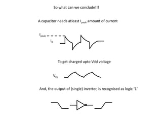
  • 1. So what can we conclude!!! A capacitor needs atleast Ipeak amount of current Ipeak IR To get charged upto Vdd voltage VCL And, the output of (single) inverter, is recognised as logic ‘1’
  • 2. Consider the amount of the switching current required For a complex block something like below
  • 3. Consider the amount of the switching current required For a complex block something like below
  • 4. Why to do? 1. If the wires were ideal, i.e. 'zero' resistance, 'zero' inductance and infinitely short, thus no issue of power distribution 3/2/2013 4
  • 5. Why to do? 1. Consider capacitance to be zero for the discussion. Rdd, Rss, Ldd and Lss are well defined values. 2. During switching operation, the circuit demands switching current i.e. peak current (Ipeak). 3. Now, due to the presence of Rdd and Ldd, there will be a voltage drop across them and the voltage at Node 'A' would be Vdd' instead of Vdd. 3/2/2013 5
  • 6. Why to do? 1. When input of the inverter switches from logic '1' to logic '0', output of inverter should switch from logic '0' to logic '1'. 2. This essentially means that the output capacitance of inverter should charge till the supply voltage Vdd'. 3. But if Vdd' goes below the noise margin, due to Rdd and Ldd, the logic '1' at the output of inverter wont be detected as logic '1' at the input of the Vdd - Vdd' = Ipeak*Rdd + Ldd * (dI/dt) circuit following the inverter. 3/2/2013 6
  • 7. Why to do? Solution 1. Keep Rdd and Rss minimum by increasing width of wire. 2. Keep peak current Ipeak and change in current dI/dt as small as possible. Ipeak = CL * Vdd / tr dI/dt = CL * Vdd / tr2 3. Limit the rise time (tr). If a circuit could run at 500 ps, its unnecessary to run the circuit at 300 ps. The largest possible value of tr should be selected. Vdd - Vdd' = Ipeak*Rdd + Ldd * (dI/dt) 3/2/2013 7
  • 8. Why to do? 1. Addition of Decoupling Capacitor in parallel with the circuit 2. Everytime the critical cell (in above daigram,an inverter) switches, it draws current from Cd , whereas, the RL network is used to replenish the charge into Cd 3/2/2013 8
  • 9. We have taken care of local communication
  • 10. We have taken care of local communication Now, Consider the below scenario
  • 11.
  • 12.
  • 14. Driver Load
  • 15. Driver Load
  • 16. Driver Load
  • 17. Driver Load
  • 18. Driver Load
  • 19. Driver Load
  • 20. Driver Load
  • 21. Driver Load
  • 22. Driver Load
  • 23. Driver Load Let us trace the path of current when Driver is ‘Switching’
  • 24. Driver Load Let us trace the path of current when Driver is ‘Switching’
  • 25. Driver Load Let us trace the path of current when Driver is ‘Switching’
  • 26. Driver Load Let us trace the path of current when Driver is ‘Switching’
  • 27. Driver Load Let us trace the path of current when Driver is ‘Switching’
  • 28. Driver Load Let us trace the path of current when Driver is ‘Switching’
  • 29. Driver Load No Decoupling Capacitors are involved in the path through ‘Blue’ line
  • 30. Driver Load Hence, switching through ‘Blue’ line will need peak current, which has to supplied by Vdd
  • 31. Driver Load And not through Decaps.
  • 32. Driver Load This will lead to ‘voltage droop’ and ‘ground bounce’, i.e. disturbance in power supply network
  • 33. Driver Load Assume, the ‘Blue’ path is a 16-bit bus
  • 34. Also assume, the 16-bit bus is having present data as below 1110010111000110
  • 35. Also assume, the 16-bit bus is having present data as below 1110010111000110
  • 36. Also assume, the 16-bit bus is having present data as below 1110010111000110
  • 37. Also assume, the 16-bit bus is having present data as below 1110010111000110 V V V V V V V V V
  • 38. Also assume, the 16-bit bus is having present data as below 1110010111000110 V V V 0 0 V 0 V V V 0 0 0 V V 0
  • 39. V V V 0 0 V 0 V V V 0 0 0 V V 0
  • 40. V V V 0 0 V 0 V V V 0 0 0 V V 0
  • 41. V V V 0 0 V 0 V V V 0 0 0 V V 0 Now, Lets the output of 16 – bit bus, is connected to an inverter
  • 42. V V V 0 0 V 0 V V V 0 0 0 V V 0 Now, Lets the output of 16 – bit bus, is connected to an inverter 1110010111000110 16-bit bus 16-bit bus
  • 43. V V V 0 0 V 0 V V V 0 0 0 V V 0 Now, Lets the output of 16 – bit bus, is connected to an inverter 1110010111000110 16-bit bus 16-bit bus 0001101000111001
  • 44. V V V 0 0 V 0 V V V 0 0 0 V V 0 0001101000111001
  • 45. V V V 0 0 V 0 V V V 0 0 0 V V 0 0001101000111001 What does this mean?
  • 46. V V V 0 0 V 0 V V V 0 0 0 V V 0 0001101000111001 What does this mean? This means, all capacitors which were charged to ‘V’ volts will have to discharge to ‘0’ volts through single ‘Ground’ tap point. This will cause a bump in ‘Ground’ tap point.
  • 47. V V V 0 0 V 0 V V V 0 0 0 V V 0 0001101000111001 What does this mean? This means, all capacitors which were charged to ‘V’ volts will have to discharge to ‘0’ volts through single ‘Ground’ tap point. This will cause a bump in ‘Ground’ tap point. V V V 0 0 V 0 V V V 0 0 0 V V 0
  • 48. V V V 0 0 V 0 V V V 0 0 0 V V 0 0001101000111001 What does this mean? This means, all capacitors which were charged to ‘V’ volts will have to discharge to ‘0’ volts through single ‘Ground’ tap point. This will cause a bump in ‘Ground’ tap point. V V V 0 0 V 0 V V V 0 0 0 V V 0
  • 49. V V V 0 0 V 0 V V V 0 0 0 V V 0 0001101000111001 What does this mean? This means, all capacitors which were charged to ‘V’ volts will have to discharge to ‘0’ volts through single ‘Ground’ tap point. This will cause a bump in ‘Ground’ tap point. V V V 0 0 V 0 V V V 0 0 0 V V 0 Ground Bounce
  • 50. V V V 0 0 V 0 V V V 0 0 0 V V 0 0001101000111001 What does this mean?
  • 51. V V V 0 0 V 0 V V V 0 0 0 V V 0 0001101000111001 What does this mean? Also, all capacitors which were ‘0’ volts will have to charge to ‘V’ volts through single ‘Vdd’ tap point. This will cause lowering of voltage at ‘Vdd’ tap point.
  • 52. V V V 0 0 V 0 V V V 0 0 0 V V 0 0001101000111001 What does this mean? Also, all capacitors which were ‘0’ volts will have to charge to ‘V’ volts through single ‘Vdd’ tap point. This will cause lowering of voltage at ‘Vdd’ tap point. V V V 0 0 V 0 V V V 0 0 0 V V 0
  • 53. V V V 0 0 V 0 V V V 0 0 0 V V 0 0001101000111001 What does this mean? Also, all capacitors which were ‘0’ volts will have to charge to ‘V’ volts through single ‘Vdd’ tap point. This will cause lowering of voltage at ‘Vdd’ tap point. V V V 0 0 V 0 V V V 0 0 0 V V 0
  • 54. V V V 0 0 V 0 V V V 0 0 0 V V 0 0001101000111001 What does this mean? Also, all capacitors which were ‘0’ volts will have to charge to ‘V’ volts through single ‘Vdd’ tap point. This will cause lowering of voltage at ‘Vdd’ tap point. Voltage Droop V V V 0 0 V 0 V V V 0 0 0 V V 0
  • 55. So what could be the solution ?
  • 56. So what could be the solution ? Driver Load
  • 57. So what could be the solution ? Driver Load How can ‘Driver’ and ‘Load’ can be brought close to each other in ‘L’ sense ?
  • 58. If ‘Driver’ and ‘Load’ have a lot of communication between them, then the power supply network must be designed in such a way, that they are Inductively close to each other
  • 59. If ‘Driver’ and ‘Load’ have a lot of communication between them, then the power supply network must be designed in such a way, that they are Inductively close to each other So, how do we design power supply distribution network?
  • 60. If ‘Driver’ and ‘Load’ have a lot of communication between them, then the power supply network must be designed in such a way, that they are Inductively close to each other So, how do we design power supply distribution network? MESH!!!!
  • 61.
  • 62. Vdd Vss Vdd Vss Vdd Vss Vss Vss Vdd Vdd Vss Vss Vdd Vdd Vss Vss Vdd Vdd Vdd Vss Vdd Vss Vdd Vss
  • 63. Vdd Vss Vdd Vss Vdd Vss Vss Vss Vdd Vdd Vss Vss Vdd Vdd Vss Vss Vdd Vdd Vdd Vss Vdd Vss Vdd Vss
  • 64. Vdd Vss Vdd Vss Vdd Vss Vss Vss Vdd Vdd Vss Vss Vdd Vdd Vss Vss Vdd Vdd Vdd Vss Vdd Vss Vdd Vss
  • 65. Power should not be coming only from one place
  • 66. Power should not be coming only from one place But from many places
  • 67. Power should not be coming only from one place But from many places Assume that, the boundary power is available, now we have to get it inside the chip
  • 68. Power should not be coming only from one place But from many places Assume that, the boundary power is available, now we have to get it inside the chip Thus, local communication is taken care by de-coupling capacitors
  • 69. Power should not be coming only from one place But from many places Assume that, the boundary power is available, now we have to get it inside the chip Thus, local communication is taken care by de-coupling capacitors And, common rail inductance coupling issue is taken care by power mesh
  • 70. DECAP1 D Block a Block b 4 DECAP2 Block c DECAP3 Die Vss Core Vdd