This report is documented for Metal Detector System. The goal is to analyze, design, model, simulate and construct the Metal Detector System. A very simple Design Pattern was used to modulate the system with the use of less number of components. Coils were designed in consideration to the principles of induction for the Metal Detector System. Standard components were used to construct the Signal Processing Unit (ASPU). The design for the ASPU was simulated and tested using advanced simulation software called Pspice. The final Product fulfills the requirements as expected.
+97470301568>> buy weed in qatar,buy thc oil qatar,buy weed and vape oil in d...
Metal Detector Project
1. 62462 Project 3 in Circuit theory and Analog
Group 4
Metal
Detector
28. maj
2014
Abstract
This report is documented for Metal Detector System. The
goal is to analyze, design, model, simulate and construct
the Metal Detector System. A very simple Design Pattern
was used to modulate the system with the use of less
number of components. Coils were designed in
consideration to the principles of induction for the Metal
Detector System. Standard components were used to
construct the Signal Processing Unit (ASPU). The design
for the ASPU was simulated and tested using advanced
simulation software called Pspice. The final Product
fulfills the requirements as expected.
Supervisor
Abdallah Ahmad Ibrahim Al-Mass
Assistant Lecturer
DTU Ballerup Campus
aalm@dtu.dk
Lars Maack
Head of studies,
Associate professor
lmaa@dtu.dk
Students:
Danish Mohammed Ali Bangash - s104712
Arier Azad Jaff - s121635
Nobert Nikolas Kruz - s127648
2. 62462 Project 3 in Circuit theory and Analog
Group 4
Note: For Schematics, Test Results and Block Diagram Of the system please refer to the appendices at the last part of the report
1
Table of Contents
1 Introduction ............................................................................................................................................... 2
1.1 Project start........................................................................................................................................ 2
1.2 Problem Formulation......................................................................................................................... 2
1.3 Milestone Plan................................................................................................................................... 3
2 Problem Analysis....................................................................................................................................... 3
3 Project Delimitation and Methods............................................................................................................. 4
3.1 Solution Strategy ............................................................................................................................... 4
3.2 Requirements..................................................................................................................................... 4
3.3 Problem Solution............................................................................................................................... 5
3.3.1 Block Diagram Representation of the System........................................................................... 5
3.3.2 Metal Object .............................................................................................................................. 5
3.3.3 AC Signal .................................................................................................................................. 5
3.3.4 Transducer Part.......................................................................................................................... 5
3.3.5 ASPU Part ................................................................................................................................. 5
3.3.6 Transducer ................................................................................................................................. 6
3.3.7 Analog Signal Processing Unit (ASPU).................................................................................... 6
3.4 Resources (Hardware / Software)...................................................................................................... 9
4 Conclusion............................................................................................................................................... 10
4.1 Product Assessment......................................................................................................................... 10
4.2 Process Assessment......................................................................................................................... 10
5 Appendixes.............................................................................................................................................. 11
5.1 Appendix 1. (Schematics)................................................................................................................ 11
5.1.1 Amplifier ................................................................................................................................. 11
5.1.2 Active Full Wave Precision Rectifier...................................................................................... 11
5.1.3 Active Low Pass Filters In Cascade ........................................................................................ 12
5.1.4 Full System Schematic ............................................................................................................ 12
5.2 Appendix 2. (Transducer Test)........................................................................................................ 13
5.3 Appendix 3. (ASPU Tests).............................................................................................................. 14
5.4 Metal Detector Test ......................................................................................................................... 15
5.5 Appendix 4. (Calculations).............................................................................................................. 16
5.5.1 Coil related calculations: ......................................................................................................... 16
3. 62462 Project 3 in Circuit theory and Analog
Group 4
Note: For Schematics, Test Results and Block Diagram Of the system please refer to the appendices at the last part of the report
2
Preface
This report is fully packed with documentation of the metal detector system. It covers the important aspects
of the product and the process of developing the System.
The problem formulated is the combination of electro physics and circuit theory to implement the system
that can be used in real life as well.
The reader of the report should have the basic knowledge and understanding of the system or any related
theory.
1 Introduction
1.1 Project start
The goals for the project is to analyze design, construct, test and simulate a metal detector system. The
System should have to be able to detect any metal object under it but only metal.
It can be used for any security purposes at the airport or any metal restricted areas, many companies
require this product too for organic processes to evaluate the metal objects contained in any organic
processes like recycling and checking for metals.
1.2 Problem Formulation
For the metal detector there will be the need of a transducer, which operates with the input which is the coin
or metal object, the transducer is powered by the function generator, transducer consist of 3 coils, which
convey one energy domain to another energy domain. Transducer operates with the frequency of 10 kHz.
Copper wire is used for the construction of the coils.
An active precision rectifier has to be used to change the AC signal to a DC signal. The reason why the
rectifier should be active is that we amplify the signal; non-active rectifier has a voltage drop over the diodes.
An active low pass filter is used which are constructed using the OP-Amps with a reason to amplify the
signal as like the rectifier. However we are using two active low pass filters on of them makes the signal
smooth but reverse and the other does the same and have a high gain before the output.
And then the signal will be reversed by each other and generate an output of 5V DC with reduced noise and
smoothens the signal.
All the modules combined together will be the metal detector system.
4. 62462 Project 3 in Circuit theory and Analog
Group 4
Note: For Schematics, Test Results and Block Diagram Of the system please refer to the appendices at the last part of the report
3
1.3 Milestone Plan
Week Number
Task 12 13 14 15 16 17 18 19 20 21 22
Project Start x
Problem Formulation x
Block diagram x
Milestone Plan x
Create Transducer x
Testing Transducer x
Create ASPU x Holidays x
Testing ASPU holidays x
Simulations x
Adjustments x x
Error Correcting x x
Finish report x x
2 Problem Analysis
For the metal detector we will need a coil for detecting the metal part. Transducer consists of one transmitter
coil and two receiving. The transmitter coil is connected to a function generator. The receiving coils are
placed inside the transmitter coil, with each in the opposite direction of each other.
By placing the receiving coils in opposite directions of each other the B-field will be nullified by each other.
The small coil is connected to the ASPU, which gives the required output. Inside ASPU the AC signal gets
amplified, by the amplifier then the output is passed on to the rectification. A low pass filter is introduced in
order to ensure the output ripple is within the requirements.
5. 62462 Project 3 in Circuit theory and Analog
Group 4
Note: For Schematics, Test Results and Block Diagram Of the system please refer to the appendices at the last part of the report
4
3 Project Delimitation and Methods
3.1 Solution Strategy
A Precision Rectifier is used, also known as the Full Wave Precision Rectifier the topology used is based on
two stages, HWR and a summing stage. Two Low Pass Filters are constructed in cascade to filter the
rectified signal the designed is properly calculated and simulated with respect to the preset requirements.
For the purpose of the induction, outer coil called the transmitter coils was mounted on the top of the plastic
plate and the inner coils called the receiver coils are placed precisely measured as fitted inside the transmitter
coils.
3.2 Requirements
Here we have specified the requirements for the metal detector.
System requirements:
Reference Test Object: A Danish “5 KRONER” coin
Reference Position: Test Object is 1 cm from the transducer at the place, and an orientation, where
the sensitivity is best.
Output DC voltage when the Reference Test Object is at its reference position: VOUT = 5 V ± 0.5 V
Output DC voltage with no metal object: VOUT = 0 V ± 0.5 V
Output peak to peak ripple voltage: Vout peak-to-peak ≤ 20 mV
Transducer requirements:
The transducer must be of type “Continuous Wave - Differential coil” operating at 10 kHz
The transducer output voltage must be zero initially and as big as possible when metal is nearby.
The transducer must be driven from a standard lab function generator with 50 ohm output resistance.
The transducer must have a flat physical design and be homemade. You must decide the number of
turns, size and geometries.
The design should be explained from electro physics formulas and sketches or simulations of the
magnetic fields
Analog Signal Processing Unit (ASPU) requirements:
The ASPU must convert the transducer output signal into a system output voltage as specified under
“System Requirements”
The transducer may pick up unwanted external noise in a broad frequency range. To reduce this
noise, the transducer + ASPU input stages, must have a 3-dB bandwidth of maximum 4 kHz
Additional requirements:
Potentiometers or variable resistors are in general unwanted, but if needed it can be accepted for fine
tuning the output voltage e.g. for sensitivity adjustment
6. 62462 Project 3 in Circuit theory and Analog
Group 4
Note: For Schematics, Test Results and Block Diagram Of the system please refer to the appendices at the last part of the report
5
3.3 Problem Solution
3.3.1 Block Diagram Representation of the System
Figure 5: Block Diagram of the System
3.3.2 Metal Object
The metal object is to be scanned on the transducer part for the purpose of metal detection.
3.3.3 AC Signal
Transducer takes Ac input from the function generator at the frequency of 10 kHz.
3.3.4 Transducer Part
Transducers were constructed by hand, transducer consist of an outer coil called the transmitter coil
and the two inner coils called the receiver coils. The coils were tested to measure the output generated
from the coil.
3.3.5 ASPU Part
The ASPU was started by designing the circuit and analyzed using simulation process, Orcad Pspice
was used for this purpose; the output of the system was verified by the simulation process.
Furthermore after the simulation process the design was implemented on a Printed Circuit Board, in
short “PCB “. The PCB was constructed twice first time it emerged with the some minor issues like
miss connections and wrong placements of the components. Second time the board was tested and
worked as expected.
7. 62462 Project 3 in Circuit theory and Analog
Group 4
Note: For Schematics, Test Results and Block Diagram Of the system please refer to the appendices at the last part of the report
6
3.3.6 Transducer
The transceiver coil generates a B-field by the 10 kHz alternating current signal form the function generator.
The two inner coils in the system are a transmitter coil and receiver coil. The inner coils will counter the B -
field with a B - field from the induced current.
This will lead to an induced current and voltage:
( )
( )
These formulas are defined by Faraday's law of electromagnetic induction.
Both inner coils will create a B - field. The B - field of the receiving coil will be opposing the B - field of the
transmitter coil due to their turning in opposite directions. It is important to design these two receiver coils of
same size and turns so that they nullify each other when there is no coin.
By holding a coin over the receiving coil a drop in voltage happens, since adding an extra B - field will
reduce the voltage.
This will lead to detection of the coin.
3.3.7 Analog Signal Processing Unit (ASPU)
3.3.7.1 Amplifier
The operational amplifier is connected with feedback to produce a closed loop operation. The
inverting amplifier circuit amplifies a voltage by a factor –R2/R1.So that the gain of the circuit can
be controlled by controlling the resistor value.
Figure 1: Screenshot of the amplified signal
8. 62462 Project 3 in Circuit theory and Analog
Group 4
Note: For Schematics, Test Results and Block Diagram Of the system please refer to the appendices at the last part of the report
7
3.3.7.2 Full Wave Precision Rectifier
In order to make the signal a positive DC signal a decision was taken to use a precision rectifier. The
precision rectifier, also known as the super diode, configuration obtained with an operational amplifier
in order to have circuit behave like an ideal diode and rectifier which are useful for high-precision
signal processing.
The rectifier is divided in two parts first part of the circuit is active when the signal is positive, for
each half cycle, one diode is forward biased, and the other is reversed biased.
The output of the first part generates a Half Wave Rectification with negative value of the double
positive input value which is added to a sine wave as an input to the second part of the Precision
Rectifier. It generates a Full Wave Rectification at the output with the negative value furthermore the
signal is added to the inverting OP-Amp and a positive full wave signal is generated.
Figure 2: Simulation shot of full wave rectification in Time Domain.
3.3.7.3 Active low Pass Filters
The use of two filters was needed to average the average of the rectified signal- the pulsating DC. The
purposed component is called cascaded active low pass filters.
The basic RC circuit principle is used for implantation of the circuit for filters. The resistor has a
constant resistance while the capacitor varies its impedance. High resistance is optimized at a very low
frequencies and a very low resistance optimized at higher frequencies.
The Filters are acting as a voltage divider,
We need to find out R=XC=10k which is the cut off frequency at -3db, is calculated using the
equation given below
9. 62462 Project 3 in Circuit theory and Analog
Group 4
Note: For Schematics, Test Results and Block Diagram Of the system please refer to the appendices at the last part of the report
8
Gain of Op-Amp Av =
Capacitor value calculated using C =
Resistance calculated using R2 =
Transfer Function for the filters
In figure below we can see the bode plot of the two low pass filters in cascade. Since the cutoff
frequency for both filters is the same, we have two poles laying at the cutoff frequency
Figure 3: Screenshot of active low pass filters in Frequency Domain
The poles Y1 and Y2 are laying at value of 41.147 DB
The Cutoff frequency is laying at 106 Hz approx. -6db. Raise time is of approx. 5ms (see figure 4).
10. 62462 Project 3 in Circuit theory and Analog
Group 4
Note: For Schematics, Test Results and Block Diagram Of the system please refer to the appendices at the last part of the report
9
Figure 4: Screenshot of active low pass filters in Time Domain
Raise time is approx. 5ms as show in the figure above marked with white line defined as 10% - 90% of the steady
state value in our case it’s the 5V
3.4 Resources (Hardware / Software)
Orcad Pspice was used to design and simulate the circuit decided for the ASPU of the Metal Detector
System.
Use of Function Generator was required to generate 10 KHz signal.
Power Supply was used to power up the Operational amplifiers at the required input voltage.
Standard Lab Oscilloscope was used to test the product and compare the simulation results with
measurements.
Standard tool box was used which contained cables for various machines.
Help from the supervisor was accessed whenever needed.
http://daycounter.com/Articles/How-To-Measure-Inductance.phtml
http://www.electronics-tutorials.ws/inductor/inductance.html
11. 62462 Project 3 in Circuit theory and Analog
Group 4
Note: For Schematics, Test Results and Block Diagram Of the system please refer to the appendices at the last part of the report
10
4 Conclusion
Part Requirement Nr Description Mandatory / Optional State
System
R1 Test object: 5 crowns Mandatory Approved
R2 Testing distance: 1 cm Mandatory Approved
R3 Max output: 4.5 V - 5.5V Mandatory Approved
R4 Min output: 0 V - 0.5 V Mandatory Approved
R5 Peak to peak: <20 mV Mandatory Approved
Transducer
R6 Operating value: 10 kHz Mandatory Approved
R7 Min output: ~ 0
Max output: 0 <
Mandatory Approved
R8 Use of function generator Mandatory Approved
R9 Handmade & calculations Mandatory Approved
R10 Formulas Mandatory Approved
ASPU R11 Convert signal Mandatory Approved
R12 3-dB bandwidth of max. 4 kHz Mandatory Approved
Additional R13 Use of potentiometers or variable
resistors
Optional Rejected
4.1 Product Assessment
The product ended up by fulfilling the expected requirements. Some of the major requirements are the
rise and fall time, +-0,5v 5v output. Approximately zero at the input when no coin is available.
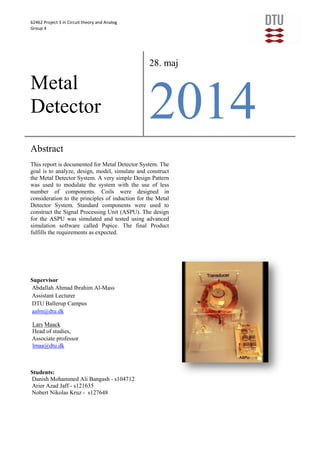
The Image at the start page is the final prototype of the Metal Detector System.
4.2 Process Assessment
It is always convenient to work with such a well-defined project who’s learning outcome is at its peak
.It is always best to particulate according to the aspects of theory. We worked according to our time
plan therefore we did not emerged with any major problems everything went very clearly though we
had some issues but not any serious technical issues. Group work was outstanding gave us a good
communication skills and understanding others work. Problem was modulated and was fairly fulfilled
by the group members.
12. 62462 Project 3 in Circuit theory and Analog
Group 4
Note: For Schematics, Test Results and Block Diagram Of the system please refer to the appendices at the last part of the report
11
5 Appendixes
5.1 Appendix 1. (Schematics)
5.1.1 Amplifier
Figure 5: Screen Shot shows the Amplification Circuit
5.1.2 Active Full Wave Precision Rectifier
13. 62462 Project 3 in Circuit theory and Analog
Group 4
Note: For Schematics, Test Results and Block Diagram Of the system please refer to the appendices at the last part of the report
12
Figure 6: Screen Shot shows the Full Wave Rectifier (active)
5.1.3 Active Low Pass Filters In Cascade
Figure 7: Screen Shot shows the Low Pass Filters in Cascade
5.1.4 Full System Schematic
Figure 8: Screen Shot shows the Schematic of the Whole System
14. 62462 Project 3 in Circuit theory and Analog
Group 4
Note: For Schematics, Test Results and Block Diagram Of the system please refer to the appendices at the last part of the report
13
5.2 Appendix 2. (Transducer Test)
Figure 9: Screenshot of transducer test when no coin in there
Figure 10: Screenshot of the transducer test when coin is introduced
15. 62462 Project 3 in Circuit theory and Analog
Group 4
Note: For Schematics, Test Results and Block Diagram Of the system please refer to the appendices at the last part of the report
14
5.3 Appendix 3. (ASPU Tests)
Figure 11: Screenshot of the Amplification test
Figure 12: Screenshot of the half wave rectification test
16. 62462 Project 3 in Circuit theory and Analog
Group 4
Note: For Schematics, Test Results and Block Diagram Of the system please refer to the appendices at the last part of the report
15
Figure 13: Screenshot of the full wave rectification test
5.4 Metal Detector Test
Figure 14: Screenshot of Metal Detector when idle
17. 62462 Project 3 in Circuit theory and Analog
Group 4
Note: For Schematics, Test Results and Block Diagram Of the system please refer to the appendices at the last part of the report
16
Figure 15: Screenshot Of the Metal Detector System when coin is introduced
5.5 Appendix 4. (Calculations)
5.5.1 Coil related calculations:
To find the inductance this formula can be used:
√
F = 10 kHz
R = 4 ohm
√
To find the number of turns of the coil this formula is used:
( )
18. 62462 Project 3 in Circuit theory and Analog
Group 4
Note: For Schematics, Test Results and Block Diagram Of the system please refer to the appendices at the last part of the report
17