Cloud Frontiers: A Deep Dive into Serverless Spatial Data and FME
G1103026268
1. IOSR Journal of Electrical and Electronics Engineering (IOSR-JEEE)
e-ISSN: 2278-1676,p-ISSN: 2320-3331, Volume 11, Issue 3 Ver. II (May. – Jun. 2016), PP 62-68
www.iosrjournals.org
DOI: 10.9790/1676-1103026268 www.iosrjournals.org 62 | Page
Power and Speed Analysis of CMOS-based Multipliers using
VEDIC techniques
Adnan Ghaderi, Javad Frounchi
Electrical and Computer Engineering Department University of Tabriz Tabriz, Iran
Electrical and Computer Engineering Department University of Tabriz Tabriz, Iran
Abstract: Multipliers are one of the most important components in design of both digital and analog circuits.
The design and structure of multipliers play a significant role to determine speed and power consumption of
processing units as the core component of electronic devices. In this paper, we design 4×4 and 8×8 multipliers
in layout level to extract important design parameters. VEDIC mathematic techniques and CMOS logic are used
to obtain a tradeoff between speed and power efficiency. Our results show that voltage range between 1.5v and
2.5v is the efficient range to perform high speed and low power multiplication.
Keywords: Multiplier; VEDIC; L-edit; CMOS; Low power
I. Introduction
Multipliers, play vital role to determine speed and power consumption of most arithmetic processes.
Due to abundant utilization of multipliers in Digital Signal Processors they have been considered as one of the
most significant elements in designing these types of processor. This significance has led several researches to
optimize multiplier’s architectures. Existing researches have shown that the main issues which should be
considered in designing a multiplier are increasing multiplier speed and decreasing power consumption.In the
recent years, a lot of work has been done to design efficient multiplier architecture based on high speed and low
power techniques.
In order to design high speed and low power multiplier, various techniques have been applied into
different architectures. In (Zhijun and Ercegovac 2005) a high performance and low power linear array
multipliers has been designed by using signal flow optimization and splitting of the reduction array into
upper/lower parts techniques. In (Mahant-Shetti, Balsara et al. 1999) a low power multiplier has been designed
by utilizing temporal tiling with array multiplier technique. In (Nagamatsu, Tanaka et al. 1990), a CMOS
multiplier with high speed performance has been presented based on improved parallel structure. In (Fadavi-
Ardekani 1993), a M×N Booth encoded parallel multiplier generator has been designed by taking advantage of
optimized Wallace trees to decrease the delay. (Kuang and Wang 2010) has used Booth technique to make
power-efficient multiplier. (Hemavathi and Rao 2015) has utilized a modified Booth recording with zero
bypassing technique to reduce power consumption. (Abu-Khater, Bellaouar et al. 1996) has designed a low
power multiplier using circuit techniques and CMOS style. In (Tiwari, Gankhuyag et al. 2008) Vedic
mathematics technique has been used to improve speed and power of multiplier. In (Thapliyal and Srinivas
2004), a high speed N×N bits parallel multiplier has been designed based on Vedic mathematics.
In order to design high speed and low power multiplier, various techniques have been applied into
different architectures. In this paper 4×4 and 8×8 CMOS multiplier are designed by making use ancient Indian
Vedic mathematics technique (Nicholas, Williams et al. 1982; Nicholas, Williams et al. 1984; Bharath and
Tirathji 1986) with respect to reducing delay and using low power architecture. The validity of the proposed
circuit is verified using Hspice in 800nm standard technology and L-Edit. The paper organized as follows: In
section II multiplier architecture is explained. In section III, the CMOS multiplier is designed. Simulation results
are presented in section IV and some conclusions are provided in section V.
II. Multiplier Architecture
A. Vedic Multiplication Algorithm
Vedic mathematics is an ancient Indian system which includes sixteen algorithms (Tiwari, Gankhuyag
et al. 2008). All algorithms have their own importance and they have been used for the multiplication of two
numbers.
Urdhva Tiryakbhyam algorithm is the most flexible method that can be used for binary multiplication.
Urdhva Tiryakbhyam means vertically and crosswise. In order to become familiar with how the algorithm
works, consider the multiplication of two binary numbers in fig. 1, which A= 11 and B= 10:
2. Power and Speed Analysis of CMOS-based Multipliers using VEDIC techniques
DOI: 10.9790/1676-1103026268 www.iosrjournals.org 63 | Page
Fig. 1. Multiplication of two binary numbers with Urdhva algorithm.
This algorithm is based on creative concept which makes possible the computation of partial product
and their sums in the same step. As shown in fig. 1, at first, we multiply the first digit of two numbers vertically,
then in step 2 we do crosswise multiplication of digits and sum of both partial products, finally in step 3, we
have to multiply second digits of two numbers vertically and add it to carry of previous section.
B. VLSI architecture by using CMOS logic Style
Utilizing low power consumption architecture in integrated circuits with large structure and area is
inevitable. The increasing demand for low power architectures, encourage researchers to test various techniques.
Power consumption reduction could be achieved in circuit level, by choosing proper logic style. CMOS is one of
the appropriate logic styles that because of its structure have been used for low power approaches. In this paper
we used Inverter, OR and AND gates based on CMOS styles. In fig. 2 and fig. 3, show these gates with true
table and layout of structures.
Fig. 2. Basic CMOS gates with true table.
Fig. 3. Layout of CMOS gates
3. Power and Speed Analysis of CMOS-based Multipliers using VEDIC techniques
DOI: 10.9790/1676-1103026268 www.iosrjournals.org 64 | Page
III. Multiplier Architecture Design
Proposed 8×8 multiplier architecture is based on product of two 8 bit numbers. Structure of 8×8
multiplier include four block of 4×4 multipliers and structure of 4x4 multiplier consist of four 2×2 block
multipliers. Architecture of 2×2, 4x4 and 8×8 multipliers are explained in following sections.
A. Architecture and Layout of 2×2 Multiplier
In implementation of proposed multiplier, a 2×2 block multiplier is the basic block. As we know in
binary multiplication, for multiply two bit, we use AND gate to multiply both bit, also use Half Adder (HA), to
add outputs of AND gates. Structure and layout of 2×2 multiplier shown in fig.4 and fig.5.
Consider two number with two bits length, which means A(A1A0) and B(B1B0). The output will be four
bits length. As shown in fig.4 and fig.5: the upper half adder, add outputs of second AND gate (A0B1) and third
AND gate (A1B0), also the lower half adder is sum between output of last AND gate (A1B1) with carry generated
in upper half adder. Finally a number with four bits length will be generated (Q3Q2Q1Q0).
Fig. 4. Structure and Layout of HalfAdder (HA).
Fig. 5. Structure and Layout of 2×2 multiplier.
4. Power and Speed Analysis of CMOS-based Multipliers using VEDIC techniques
DOI: 10.9790/1676-1103026268 www.iosrjournals.org 65 | Page
B. Architecture and Layout of 4×4 Multiplier
When input bit length increase, structure of multiplier will change. For multiplication of two numbers,
separate each input number into two equal parts. For implementation of 4×4 multiplier consider two inputs such
A(A3A2A1A0) and B(B3B2B1B0), the result of multiplication is eight bits as Q(Q7 Q6 Q5 Q4 Q3 Q2 Q1 Q0).
Firstly, A and B should be divided into two equal parts, which A1A0 and A3A2 as A, also B1B0 and B3B2 as
B. After dividing two bits multiplication should be done simultaneously and by four blocks of 2×2 multiplier.
The first 2×2 multiplier block uses A1A0 and B1B0 as input, the second one feed with A1A0 and B3B2 the
third one takes A3A2 and B1B0 and last one works with A3A2 and B3B2.
Secondly, all of the 2×2 multipliers block outputs in a specific structure should be linked to two four
bits ripple carry adders and two half adder and one OR gate, just like fig.7. Layout of 4×4 multiplier is
represented in fig.8.
Fig. 6. Structure of Full Adder and 4-bits Ripple carry adder.
Fig. 7. Structure of 4×4 multiplier.
5. Power and Speed Analysis of CMOS-based Multipliers using VEDIC techniques
DOI: 10.9790/1676-1103026268 www.iosrjournals.org 66 | Page
Fig. 8. Layout of 4×4 multiplier
C. Architecture and Layout of 8×8 Multiplier
The structure of 8×8 multiplier is somehow the same as the structure of 4×4 multiplier with a little
difference and extension. The proposed 8×8 multiplier uses four 4x4 block multiplier. We implement 8×8
multiplier with two eight bits numbers, A(A7-A0) and B(B7-B0), and its sixteen bits output Q(Q15-Q0). The
structure of this multiplier is shown in fig.9. Its layout is also shown in fig.10.
Fig. 9. Structure of 8×8 multiplier.
6. Power and Speed Analysis of CMOS-based Multipliers using VEDIC techniques
DOI: 10.9790/1676-1103026268 www.iosrjournals.org 67 | Page
Fig. 10. Layout of 8×8 multiplier
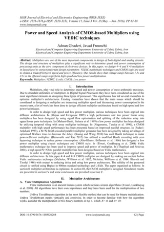
IV. Result
In this work, layout of multiplier design with L-edit v8.30 and simulate with Hspice. In this paper, in
order to calculate the power, we use the source average current times the voltage in one period. Additionally,
considering the architecture of the circuit as shown in fig.9, for calculating the delay we tried to choose the
longest path with biggest number of blocks. In order to stimulate the circuit in a way that output is also changed,
and as a result calculation of delay and power is made easier for us, for both states of the multiplier we used a
variable pulse source. We have considered the worst case scenario in picking the numbers to be multiplied,
resulting in two numbers with all the bits of 1. Bearing in mind that all the bits in 4×4 and 8×8 are 1 and due the
architecture of the circuit, q3 and q7 have been respective chosen for the delay of 4×4 and 8×8. Table I and table
II show the results of simulation for 4×4 and 8×8 multipliers. Power consumption and delay for both multipliers
at 50MHz and 100MHz are shown in table I and table II with voltage supply of 1v, 1.5v, 2v and 3v. This
multiplier doesn’t work correctly for 1v supply, also power consumption will increase for high voltages but
delay will decrease. So based on our requirements, we can chose proper supply.
Table 1. Power and delay in 50 MHZ
Propose paper
Freq. = 50
MHz
Supply
1v 1.5 2 v 2.5v 3 v
Power
(mW)
Delay
(ns)
Power
(mW)
Delay
(ns)
Power
(mW)
Delay
(ns)
Power
(mW)
Delay
(ns)
Power
(mW)
Delay
(ns)
4×4 Multiplier 0.17 --- 2 21 5.14 13 9.5 11 14.8 9
8×8 Multiplier 0.25 --- 4.59 32 13.6 20 26.7 15 43.8 12
Table 2. Power and delay in 100 MHZ
Propose
paper
Freq. =
100
MHz
Supply
1v 1.5 2 v 2.5v 3 v
Power
(mW)
Delay
(ns)
Power
(mW)
Delay
(ns)
Power
(mW)
Delay
(ns)
Power
(mW)
Delay
(ns)
Power
(mW)
Delay
(ns)
4×4
Multiplier
0.1 --- 1.93 19.5 6.18 12.5 12.3 10.5
21.5 9
8×8
Multiplier
0.12 --- 3.73 23 13.7 18.5 29.5 16.5
53.3 12
V. Conclusion
This paper presents 4×4 and 8×8 multiplier by taking advantage of ancient Indian Vedic mathematics
technique with respect to reducing delay and also used CMOS logic based to reduce power consumption. After
designing layout and simulating it, we understand proper voltage range is between 1.5v to 2.5v. Because of
lower range, multiplier doesn’t work correctly and also for higher range, power consumption will be increased.
For future works, we can select different styles in circuit level to decrease area.
7. Power and Speed Analysis of CMOS-based Multipliers using VEDIC techniques
DOI: 10.9790/1676-1103026268 www.iosrjournals.org 68 | Page
References
[1]. Abu-Khater, I. S., A. Bellaouar, et al. (1996). "Circuit techniques for CMOS low-power high-performance multipliers." IEEE
Journal of Solid-State Circuits 31(10): 1535-1546.
[2]. Bharath, J. S. S. and K. Tirathji (1986). "Vedic Mathematics or Sixteen Simple Sutras From The Vedas." Motilal Banarsidas,
Varanasi (India).
[3]. Fadavi-Ardekani, J. (1993). "M* N Booth encoded multiplier generator using optimized Wallace trees." Very Large Scale
Integration (VLSI) Systems, IEEE Transactions on 1(2): 120-125.
[4]. Hemavathi, K. and G. M. Rao (2015). Empirical Analysis of Low Power and High Performance Multiplier. Computational
Intelligence in Data Mining-Volume 2, Springer: 585-594.
[5]. Kuang, S. R. and J. P. Wang (2010). "Design of Power-Efficient Configurable Booth Multiplier." IEEE Transactions on Circuits
and Systems I: Regular Papers 57(3): 568-580.
[6]. Mahant-Shetti, S. S., P. T. Balsara, et al. (1999). "High performance low power array multiplier using temporal tiling." IEEE
Transactions on Very Large Scale Integration (VLSI) Systems 7(1): 121-124.
[7]. Nagamatsu, M., S. Tanaka, et al. (1990). "A 15-ns 32×32-b CMOS multiplier with an improved parallel structure." IEEE
Journal of Solid-State Circuits 25(2): 494-497.
[8]. Nicholas, A., K. Williams, et al. (1982). "Lectures on Vedic Mathematics." Spiritual Study Group, Roorkee (India).
[9]. Nicholas, A., K. Williams, et al. (1984). "Application of Urdhava Sutra." Spiritual Study Group, Roorkee (India).
[10]. Thapliyal, H. and M. Srinivas (2004). "High Speed Efficient N x N Bit Parallel Hierarchical Overlay Multiplier Architecture Based
on Ancient Indian Vedic Mathematics." Enformatika Trans 2: 225-228.
[11]. Tiwari, H. D., G. Gankhuyag, et al. (2008). Multiplier design based on ancient Indian Vedic Mathematics. SoC Design Conference,
2008. ISOCC '08. International.
[12]. Zhijun, H. and M. D. Ercegovac (2005). "High-performance low-power left-to-right array multiplier design." IEEE Transactions on
Computers 54(3): 272-283.