Morphing Aircraft Workshop 26/03/13 - Presentation on Auxetics
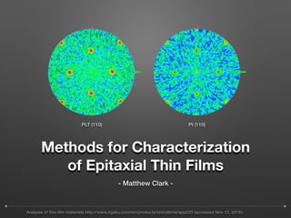
Methods for Characterization of Epitaxial Thin Films Using XRD
1. Methods for Characterization
of Epitaxial Thin Films
- Matthew Clark -
PLT (110) Pt (110)
Analysis of thin film materials http://www.rigaku.com/en/products/xrd/ultima/app033 (accessed Nov 15, 2016).
2. Thin Films
• Crucial to the success of
modern electronic devices
• Allows for complex layering in
devices
• Many different deposition
techniques: PLD, ALD,
Sputtering, Spin coating etc.
Substrate (mm)
Deposited Thin Film (nm - μm)
3. Epitaxy
• Perfectly epitaxial thin films
consist of ordered crystallite
domains matching the
structure of the underlying
substrate
• Necessary to maximize
desired properties of
anisotropic materials
Substrate
Film
Polycrystalline Film
Epitaxial Film
Substrate
Film
4. Pole Figure Diagrams
• X(α), φ(β) scan
• Used to determine degree of
preferred orientation
• Pole figures are measured along
varying crystallographic
orientations
• Tailoring of preferred orientation
crucial to device engineering
Polycrystalline Randomly Oriented
Polycrystalline Degree of Orientation
Crystallographic Texture http://www.doitpoms.ac.uk/tlplib/crystallographic_texture/texture_representation.php (accessed Nov 18, 2016).
5. Relationship Between Film
and Substrate
• Heteroepitaxy
• If lattice mismatch between film and substrate is small material
can conform to substrate
• Relaxation can create dislocations or defects
Res, H.; Zimmerman, M. High Resolution X-ray Diffractometry. www.bruker-webinars.com.
6. Reciprocal Space Mapping
• 2θ/ω , ω2θχ/φ , φ scan
• 2D representation of 3D
intensity data
• Allows for characterization
of lattice distortion/
relaxation
• Epitaxial orientation
(Mosaicity)
Konya, T. The Rigaku Journal 2009, 25 (2).
7. In Plane Diffraction
• 2θχ/φ , φ scan
• Reflection Intensities of thin
film often weak with respect
to substrate
• Diffraction from lattice planes
normal to the substrate
observed
• Measurement depth is
controllable
Kobayashi, S. The Rigaku Journal 2010, 26 (1).
8. Current Work
• In situ determination of lattice strain pole figures (Kazimirov et al.)
• Employing lattice strain helps to develop modeling methodology
capable of predicting alloy behavior
• In situ growth studies using synchrotron radiation (Kawamura et al.)
• Diffraction experiments performed at elevated temperatures
throughout growth stage
• Synchrotron study of microstructure gradient in laser additively formed
epitaxial Ni-based superalloy (Chen et al.)
• Laser additive formation, preferred orientation sometimes may
deviate from the axial direction of the actual growth
9. References
• Li, X.; Sundaram, S.; Disseix, P.; Gac, G. L.; Bouchoule, S.; Patriarche, G.; Réveret, F.; Leymarie, J.; Gmili, Y. E.;
Moudakir, T.; Genty, F.; Salvestrini, J.-P.; Dupuis, R. D.; Voss, P. L.; Ougazzaden, A. Optical Materials Express
2015, 5 (2), 380.
• Analysis of thin film materials http://www.rigaku.com/en/products/xrd/ultima/app033 (accessed Nov
15, 2016).
• Crystallographic Texture http://www.doitpoms.ac.uk/tlplib/crystallographic_texture/
texture_representation.php (accessed Nov 18, 2016).
• Res, H.; Zimmerman, M. High Resolution X-ray Diffractometry. www.bruker-webinars.com.
• Kobayashi, S. The Rigaku Journal 2010, 26 (1).
• Inaba, K. The Rigaku Journal 2008, 24 (1).
• Konya, T. The Rigaku Journal 2009, 25 (2).
• Mitsunaga, T. The Rigaku Journal 2009, 25 (1).
• Nagao, K.;Kagami, E The Rigaku Journal 2011, 27 (2).
• Xue, J.; Zhang, A.; Li, Y.; Qian, D.; Wan, J.; Qi, B.; Tamura, N.; Song, Z.;
Chen, K. Sci. Rep. Scientific Reports 2015, 5, 14903.
• Miller, M. P.; Bernier, J. V.; Park, J.-S.; Kazimirov, A. Review of Scientific Instruments 2005,
76 (11), 113903.
• Lamberti, C. Surface Science Reports 2004, 53 (1-5), 1–197.
• T. Kawamura, Y. Watanabe, S. Fujikawa, S. Bhunia, K. Uchida, J. Matsui, Y. Kagoshima, Y. Tsusaka,
Real-time observation of surface morphology of indium phosphide MOVPE growth with using X-ray
reflectivity technique, J. Cryst. Growth 237 (2002) 398