I have prepared it to create an understanding of delay modeling in VLSI.
Regards,
Vishal Sharma
Doctoral Research Scholar,
IIT Indore
vishalfzd@gmail.com
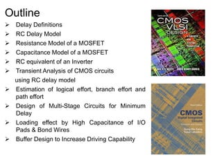
1. Outline
Delay Definitions
RC Delay Model
Resistance Model of a MOSFET
Capacitance Model of a MOSFET
RC equivalent of an Inverter
Transient Analysis of CMOS circuits
using RC delay model
Estimation of logical effort, branch effort and
path effort
Design of Multi-Stage Circuits for Minimum
Delay
Loading effect by High Capacitance of I/O
Pads & Bond Wires
Buffer Design to Increase Driving Capability
2. Basic Delay Definitions:
Propagation delay time, tpd = time difference of the input crossing 50% and
the output crossing 50% of its maximum stable value for worst case
Contamination delay time, tcd = time difference for the input crossing 50%
and the output crossing 50% of its maximum stable value for best case
Rise time, tr = time for a waveform to rise from 10% to 90% of its steady-
state value
Fall time, tf = time for a waveform to fall from 90% to 10% of its steady-state
value
Propagation delay = (tphl + tplh) / 2
For both the worst or best case,
propagation delay can be determined
from the corresponding values of tphl
and tplh for that case.
3. RC delay Model for MOSFET
Here, 𝑅 𝑛 is channel resistance of nMOS which is a function of biasing voltage
and given as: 𝑹 𝒏 =
𝑽 𝑫𝑺
𝑰 𝑫
But for the linear region of nMOS,
𝑉𝐺𝑆 > 𝑉𝑇𝑛 and 𝑉𝐷𝑆 > 0 but very small:
Then, 𝐼 𝐷 = µ 𝑛 𝐶 𝑜𝑥
𝑊
𝐿
(𝑉𝐺𝑆 − 𝑉𝑇𝑛)𝑉𝐷𝑆
Hence, 𝑹 𝒏 = 𝟏/ µ 𝒏 𝑪 𝒐𝒙
𝑾
𝑳
(𝑽 𝑮𝑺 − 𝑽 𝑻𝒏)
For the triode region of nMOS,
𝑉𝐺𝑆 > 𝑉𝑇𝑛 and 0 < 𝑉𝐷𝑆 < 𝑉𝐺𝑆 − 𝑉𝑇𝑛
Then, 𝐼 𝐷 is given as: 𝐼 𝐷 = µ 𝑛 𝐶 𝑜𝑥
𝑊
𝐿
[ 𝑉𝐺𝑆 − 𝑉𝑇𝑛 𝑉𝐷𝑆 −
𝑉 𝐷𝑆
2
2
]
Resistance R and Capacitance C of
MOSFETs are very important to decide
the transient performance of MOS
circuits
RC model for a single nMOS, of k times
than unit size, is show in figure
4. Hence, 𝑹 𝒏 = 𝟐/{µ 𝒏 𝑪 𝒐𝒙
𝑾
𝑳
𝟐 𝑽 𝑮𝑺 − 𝑽 𝑻𝒏 − 𝑉𝐷𝑆 }
The saturation region of nMOS is given as:
𝑉𝐺𝑆 > 𝑉𝑇𝑛 and 𝑉𝐷𝑆 > 𝑉𝐺𝑆 − 𝑉𝑇𝑛
Then, 𝐼 𝐷 =
1
2
µ 𝑛 𝐶 𝑜𝑥
𝑊
𝐿
[ 𝑉𝐺𝑆 − 𝑉𝑇𝑛
2]
Hence, 𝑹 𝒏 = 𝟐𝑉𝐷𝑆/ µ 𝒏 𝑪 𝒐𝒙
𝑾
𝑳
𝑉𝐺𝑆 − 𝑉𝑇𝑛
2
The generalized model of channel
resistance, independent of its
operating region for nMOS is given
as:
𝑹 𝒏 = 𝟏/ 𝜷 𝒏(𝑽 𝑫𝑫 − 𝑽 𝑻𝒏)
- where, 𝜷 𝒏 = µ 𝒏 𝑪 𝒐𝒙
𝑾
𝑳
The similar method is applied for the
pMOS device resistance modelling.
5. In general, the channel resistance for the nMOS and pMOS dependent on the
gate to source voltage can be written as:
𝑹 𝒏 ∝ 𝟏/ µ 𝒏 𝑪 𝒐𝒙
𝑾
𝑳 𝒏
(𝑽 𝑮𝑺 − 𝑽 𝑻𝒏)
𝑹 𝒑 ∝ 𝟏/ µ 𝒑 𝑪 𝒐𝒙
𝑾
𝑳 𝒑
(𝑽 𝑺𝑮 − |𝑽 𝑻𝒑|)
where, 𝐶 𝑜𝑥=
ε 𝑜𝑥
𝑡 𝑜𝑥
is a process constant which is oxide capacitance per unit
area (F/cm2).
From the above equations it is clear that:
- 𝑹 𝒏 ∝ 𝟏/𝑾 (hence, higher the width lesser would be the resistance)
- Also, the resistance varies with the gate voltage as shown in the figure.
- If we assume 𝑾 𝒏 = 𝑾 𝒑 and 𝑽 𝑻𝒏 = |𝑽 𝑻𝒑|, then 𝑹 𝒏 < 𝑹 𝒑
- It is so because, µ 𝒏 > µ 𝒑
- Therefore, to match the resistance we have to increase 𝑊𝑝
Approximate channel resistance of MOS
Resistance dependence with sizing and voltage
6. Capacitance for RC model
Here we develop the basic idea of capacitance value of nMOS for the RC
modelling.
Basically the capacitance is divided in to two parts:
Gate oxide related capacitance (𝐶 𝐺𝑆, 𝐶 𝐺𝐷)
Junction capacitance (𝐶 𝐷𝐵, 𝐶𝑆𝐵)
Gate oxide capacitance (𝐶 𝐺): It is developed due to
the overlap of gate electrode and channel charge.
𝑪 𝑮 = 𝑪 𝒐𝒙 𝐖 𝐋 where, 𝐶 𝑜𝑥=
ε 𝑜𝑥
𝑡 𝑜𝑥
- This 𝐶 𝐺 is equally split between 𝐶 𝐺𝑆 and 𝐶 𝐺𝐷 such that:
𝐶 𝐺𝑆 =
1
2
𝐶 𝑜𝑥 𝑊 𝐿 and 𝐶 𝐺𝐷 =
1
2
𝐶 𝑜𝑥 𝑊 𝐿
Also, the gate electrode overlaps the source and drain region at the edges and
results into overlap capacitances:
𝐶 𝐺𝑆(𝑜𝑣𝑒𝑟𝑙𝑎𝑝) = 𝐶 𝑜𝑥 𝑊 𝐿 𝐷 and 𝐶 𝐺𝐷(𝑜𝑣𝑒𝑟𝑙𝑎𝑝) = 𝐶 𝑜𝑥 𝑊𝐿 𝐷
- here 𝐿 𝐷 is the channel overlapping length at one end.
Therefore, the resultant gate capacitance is given as:
𝑪 𝑮𝑺 =
𝟏
𝟐
𝑪 𝒐𝒙 𝑾 𝑳 + 𝑪 𝒐𝒙 𝑾 𝑳 𝑫 and 𝑪 𝑮𝑫 =
𝟏
𝟐
𝑪 𝒐𝒙 𝑾 𝑳 + 𝑪 𝒐𝒙 𝑾 𝑳 𝑫
7. Junction Capacitance
It appears due to the diffusion of drain and source regions which create
depletion regions near the substrate and the channel stop implants.
The capacitances for the surface 1 and 5, in the figure, are given as:
𝑪𝒋𝒖𝒏 = 𝑪𝒋 𝑨𝒋𝒖𝒏
where, 𝐶𝑗 is junction capacitance per unit area (F/cm2) and 𝐴𝑗𝑢𝑛 is junction area (cm2) .
The junction capacitances for the diffusion surfaces (2, 3 and 4) which are in
contact with the highly doped channel stop implants are given as:
𝑪 𝒔𝒘 = 𝑪𝒋𝒔𝒘 𝑷 𝒔𝒘
here, 𝑪𝒋𝒔𝒘 = 𝑪𝒋 𝒙𝒋 (F/cm), 𝒙𝒋 is junction depth and 𝑷 𝒔𝒘 is the surface perimeter
(cm).
Therefore, the total junction capacitance is
given as:
𝑪𝒋𝒕𝒐𝒕𝒂𝒍 = 𝑪𝒋𝒖𝒏 + 𝑪 𝒔𝒘
It leads to total source and drain junction
capacitance as:
𝑪 𝑺𝑩(𝒔𝒐𝒖𝒓𝒄𝒆 − 𝒃𝒖𝒍𝒌) = 𝑪𝒋 𝑨 𝑺𝒋𝒖𝒏 + 𝑪𝒋𝒔𝒘 𝑷 𝑺𝒔𝒘
𝑪 𝑫𝑩(𝒅𝒓𝒂𝒊𝒏 − 𝒃𝒖𝒍𝒌) = 𝑪𝒋 𝑨 𝑫𝒋𝒖𝒏 + 𝑪𝒋𝒔𝒘 𝑷 𝑫𝒔𝒘
8. Capacitance dependence on sizing
The gate capacitance increases with the increasing size of the device.
Hence, for a MOSFET with k times of unit width will have gate capacitance
k𝑪 𝑮.
Diffusion capacitance also increases proportional to the device width.
However, Increasing channel length increases gate capacitance
proportionally but does not affect diffusion capacitance.
The overall capacitance (gate capacitance and diffusion capacitance)
can be partitioned into 𝑪 𝑮, 𝑪 𝑺 and 𝑪 𝑫 as shown below:
9. Resultant RC delay Model for a MOSFET
The equivalent RC delay models for nMOS and pMOS devices of width k are
shown in figure below.
where resistance 𝑹 𝒏 ∝ (
𝑳
𝑾
) and 𝑪 ∝ 𝐖
Here, pMOS has twice the resistance than nMOS because holes mobility (µ 𝒑) is
approx. half of the electron mobility (µ 𝒏) and
𝑹 ∝ 𝟏/µ
To make the equal resistance of nMOS and pMOS, we have to double the
width of pMOS.
10. Calculate the load capacitance at
the output node B of inverter X1?
It can be determined by estimating the
individual terminal capacitances and
then calculating the equivalent effect
of them on node B, as shown in
figures below:
wire capacitance from
output of X1 to input of X2
11. RC Equivalent of an Inverter
Below is the equivalent circuit for a fanout-of-1 inverter, when we have
neglected the wire capacitance.
- Fanout-of-1: means when the inverter is driving one similar inverter gate at the load.
The given inverter is composed of nMOS of unit size and pMOS of twice width
of unit size to exhibit equal rise and fall current/resistance.
when input is logic 1.
Hence nMOS is ON and
pMOS is OFF
Fanout-of-4 (FO4) Inverter
Output capacitance = 𝟐𝑪 + 𝑪 + 𝟒 𝟐𝑪 + 𝑪 = 𝟏𝟓𝑪
Fanout-of-1 (FO1) Inverter
12. Transient response from the RC delay model
Once the RC model is determined from the CMOS
inverter, it can easily be analysed for the transient
response.
The transfer function of this first order RC model
driven by a step input :
𝐻 𝑠 =
1
(1+𝑠𝑅𝐶)
By taking the inverse Laplace transform of H(s), the
step response:
𝑉𝑌 𝑡 = 𝑉𝐷𝐷 𝑒− 𝑡 τ where 𝜏 = 𝑅𝐶
Now, the propagation delay 𝑡 𝑝𝑑 is the time at which
the output 𝑉𝑌 reaches to 𝑉𝐷𝐷/2. Hence,
𝑉𝐷𝐷/2 = 𝑉𝐷𝐷 𝑒− 𝑡 𝑝𝑑 𝑅𝐶
It gives: 𝑡 𝑝𝑑 = 𝑅𝐶 𝑙𝑛2 𝑡 𝑝𝑑 ∝ 𝑅𝐶
Note: Delay increases with the increasing value of both R and C.
13. Design of a 3-input NAND gate for effective rise and fall
resistance equal to that of a unit inverter (R):
For worst case, only
single pMOS will be
ON, which is
equivalent to that of
a unit inverter
Width is 3 times due
to series connection:
(R/3 + R/3 + R/3
= R)
Capacitance gets increased
3 times due to increased
device width
14. Capacitances connected to the o/p terminal Y are combined
together (2C+2C+2C+3C=9C)
In similar manner, gate capacitances are detemined.
Design of a 3-input NAND gate for effective rise and fall
resistance equal to that of a unit inverter (R)…
15. RC equivalent delay model for 3-input NAND
Gate
RC equivalent when
output is falling
RC equivalent when output is rising
in worst case
In the worst case of output falling transition, output pulls
down through the three series nMOS transistors.
During the worst case of rising transition, two pMOS
remains off and one is ON. Accordingly, upper two nMOS
are still ON and bottom one is OFF.
Hence, the series capacitances of upper two nMOS must
also be discharged during the falling transition in worst
case.
16. Elmore Delay model to solve RC equivalent
delay models
RC equivalent models of the CMOS circuits can be solved by using the Elmore’s
delay model:
𝒕 𝒑𝒅 = 𝒏𝒐𝒅𝒆−𝒊 (𝑹𝒊−𝒕𝒐−𝒔𝒐𝒖𝒓𝒄𝒆 𝑪𝒊)
= 𝑹 𝟏 𝑪 𝟏 + (𝑹 𝟏+𝑹 𝟐)𝑪 𝟐 + ⋯ (𝑹 𝟏+𝑹 𝟐 + 𝑹 𝟑 … +𝑹 𝑵)𝑪 𝑵
17. Delay Modelling for a 2-input NAND Gate with Fan-
out of h (FOh)
𝑡 𝑝𝑑𝑟 = (6 + 4ℎ)𝑅𝐶 𝑡 𝑝𝑑𝑑 =
𝑅
2
2𝐶 +
𝑅
2
+
𝑅
2
6 + 4ℎ 𝐶
= (7 + 4ℎ)𝑅𝐶
Worst case Rising delay:
Worst case Falling delay:
Note: In both the cases, delay has two components (i) Independent of load
capacitance (here 6 or 7 RC) (ii) Due to external loading (4hRC)
18. Delay of a Gate as a Process-Independent Unit
(Normalized Delay 𝒅)
𝒅 =
𝒅 𝒂𝒃𝒔
𝝉
where 𝜏 = 3𝑅𝐶 is the delay of an inverter driving an identical
inverter (FO1 inverter) with no parasitic capacitance
Delay d has two components: 𝒅 = 𝒇 + 𝒑
𝒇 is Effort Delay or Stage Effort which is due to the external loading
𝒑 is Parasitic delay due to the internal capacitance when gate driving no load
(total capacitance appearing at the output terminal divided by that of unit
inverter)
Stage effort 𝒇 = 𝒈. 𝒉
Logic Effort (𝒈): Ratio of input capacitance of a gate to that of an inverter
capable of delivering the same output current:
𝒈 =
𝑪𝒊𝒏,𝒈𝒂𝒕𝒆
𝑪𝒊𝒏,𝒖𝒏𝒊𝒕_𝒊𝒏𝒗
Electrical Effort (𝒉): A gate driving h copies of itself is said to have a fan
out or electrical effort of h, which is the ratio of output capacitance and input
capacitance of the gate: 𝒉 =
𝑪 𝒐𝒖𝒕
𝑪 𝒊𝒏,𝒈𝒂𝒕𝒆
19. Then, the Effort delay: 𝑓 = 𝑔. ℎ =
𝑪 𝒊𝒏,𝒈𝒂𝒕𝒆
𝑪 𝒊𝒏,𝒖𝒏𝒊𝒕_𝒊𝒏𝒗
𝑪 𝒐𝒖𝒕
𝑪 𝒊𝒏,𝒈𝒂𝒕𝒆
=
𝑪 𝒐𝒖𝒕
𝑪 𝒊𝒏,𝒖𝒏𝒊𝒕_𝒊𝒏𝒗
Hence, the delay due to the external loading only:
𝑑(𝑎𝑏𝑠)_𝑒𝑥𝑡 = 𝑔. ℎ. τ =
𝑪 𝒐𝒖𝒕
𝑪 𝒊𝒏,𝒖𝒏𝒊𝒕_𝒊𝒏𝒗
3𝑅𝐶
=
𝑪 𝒐𝒖𝒕
𝑪𝒊𝒏,𝒖𝒏𝒊𝒕 𝒊𝒏𝒗
𝑅 𝑪𝒊𝒏,𝒖𝒏𝒊𝒕 𝒊𝒏𝒗
= 𝑪 𝒐𝒖𝒕 𝑹
𝒅(𝒂𝒃𝒔)_𝒆𝒙𝒕 = 𝑪 𝒐𝒖𝒕 𝑹
Delay of a Gate as a Process-Independent Unit
(Normalized Delay 𝒅)…
Note: delay part due to the external loading is proportional to the load
capacitance (𝑪 𝒐𝒖𝒕).
21. Gate Type Number of Inputs
1 2 3 4 N
Inverter 1
NAND 4/3 5/3 6/3 (n+2)/3
NOR 5/3 7/3 9/3 (2n+1)/3
MUX 2 2 2 2 2
XOR/XNOR 4 6 8
Logical Effort of Basic Gates
Parasitic Delay of Basic Gates
Gate Type Number of Inputs
1 2 3 4 N
Inverter 1
NAND 2 3 4 n
NOR 2 3 4 n
MUX 2 4 6 8 2n
22. Frequency of a Ring Oscillator
Delay 𝑑 = 𝑔. ℎ + 𝑝
Logical effort 𝑔 = 1
Electrical Effort ℎ = 1
Parasitic Delay 𝑝 = 1
Delay of each stage 𝑑 = 𝑔. ℎ + 𝑝 = 1 ∗ 1 + 1 = 2
Now, N-stage ring oscillator has a period of 2N stage delays because a value must
propagate twice around the ring to regain the original polarity. Therefore, the total
period of this oscillator is:
𝑇 = 2𝑁. 𝑑 = 4𝑁
Hence, the frequency of operation is: f =
1
𝑇
= (1/4𝑁)
24. Logical Effort of Paths and Path Delay
Overall path effort is given as:
𝑭 = 𝑮𝑩𝑯
Path logical effort G is the products of the logical efforts
of each stage along the path having i number of stages:
𝐺 = 𝑔𝑖
Path electrical effort H is the ratio of the output
capacitance the path must drive divided by the input
capacitance presented by the path:
𝐻 =
𝐶 𝑜𝑢𝑡(𝑝𝑎𝑡ℎ}
𝐶𝑖𝑛(𝑝𝑎𝑡ℎ)
Path branching effort B is the product of the branching
efforts between stages:
𝐵 = 𝑏𝑖
where, branching effort b is the ratio of the total capacitance
seen by a stage to the capacitance on the path:
𝑏 =
𝐶 𝑜𝑛(𝑝𝑎𝑡ℎ} + 𝐶 𝑜𝑓𝑓(𝑝𝑎𝑡ℎ}
𝐶 𝑜𝑛(𝑝𝑎𝑡ℎ)
=
15 + 15
15
= 2
Now, the Path delay D is the sum of the delays of each stage, or It can be written
as the sum of the path effort delay 𝐷 𝐹 and path parasitic delay P:
𝑫 = 𝒅𝒊 = 𝑮𝑩𝑯 + 𝑷 where, 𝑃 = 𝑝𝑖
25. Logical Effort of Paths and Path Delay…
The path delay is minimized when each stage bears the same effort.
If a path has N stages and each bears the same effort, that the stage effort must
be:
𝒇 = 𝒈𝒊 𝒉𝒊 = 𝑭 𝟏 𝑵
Thus, the minimum possible delay of an N-stage path with path effort F and path
parasitic delay P is:
𝑫 = 𝑵𝑭 𝟏 𝑵 + 𝑷
This is a key result of Logical Effort. It shows that the minimum delay of the path
can be estimated knowing only the number of stages, path effort, and parasitic
delays without the need to assign transistor sizes.
26. Estimate the minimum delay of the
path from A to B, and determine the
required Gate sizes
Path logical effort is: G = 4/3 x 5/3 x 5/3 = 100/27
Path electrical effort is: H = 45/8
Path branching effort is: B = (1+2)/1 x (1+1)/1 = 3 x 2 = 6
The path effort is: F = GBH = 100/27 x 6 x 45/8 = 125
Now, for the minimum path delay, the best stage effort is:
𝒇 = (125)1/3 = 5
Path parasitic delay is: P = 2 + 3 + 2 = 7
Hence, the minimum path delay is: D = N 𝒇 + P = 3 x 5 + 7 = 22
Now, to determine the size of various gates for min. delay:
𝒇 = 𝒈𝒊 𝒉𝒊 = 𝒈𝒊
𝑪 𝒐𝒖𝒕,𝒊
𝑪 𝒊𝒏,𝒊
=> 𝑪𝒊𝒏,𝒊 = 𝒈𝒊
𝑪 𝒐𝒖𝒕,𝒊
𝒇
Hence, working backward along the path: size y = (5/3)x(45/5) = 15
x = (5/3)x(15+15)/5 = 10
27. Delay analysis through the simulation for a
FO3-Inverter
Two methods for a Fan-out 3 Inverter is shown below:
1. The inverter working as the load has device sizes three times of the device size
for unit inverter
2. Three unit inverters are connected at the load of unit inverter
FO3 Inverter: Method 1
FO3 Inverter: Method 2
28. Delay analysis through the simulation for a
FO3-Inverter…
From the simulation: τ 𝑝𝐻𝐿 = 117.484𝑝𝑆, τ 𝑝𝐿𝐻 = 176.403𝑝𝑆
Hence, τ 𝐹𝑂3 =(τ 𝑝𝐻𝐿 + τ 𝑝𝐿𝐻)/2 = 146.94𝑝𝑆
Since, it is the delay of FO3 inverter, then the unit inverter delay:
τ =
τ 𝐹𝑂3
4
= 36.735𝑝𝑆
Transient simulation
result of FO3 Inverter
29. Logical Effort and Parasitic Delay Estimation
using simulation
The delay of a gate is given as: 𝑑𝑒𝑙𝑎𝑦 = 𝑔ℎ + 𝑝
From the previous result of FO3 Inverter,
τ 𝐹𝑂3= 146.94𝑝𝑆 = 𝑔ℎ1 + 𝑝 (1)
Now, by simulating the FO1 Inverter (as shown below, which has the same unit
inverter connected at the load), τ 𝐹𝑂1= 94.06𝑝𝑆 = 𝑔ℎ2 + 𝑝 (2)
FO1 Inverter
By solving Eq. (1) and (2), we get:
Logical Effort (g) = 26.44 pS
Parasitic Delay (p) = 67.62 pS
https://www.engr.usask.ca/classes/CME/342/lab_files/CME
342_lab4_logic_effort.pdf
30. Driver/Buffer Design for I/O Pads and Bond wire
loading affect
The delay (RC) for any circuit is increased with
the increasing load capacitance.
The excessive load (as shown by CL) may
disturb the circuit functionality. It is due to the
time taken to charge/discharge the output load
capacitance.
Now, think about the I/O pads and bond wire
loading effect with a huge size (see figures). It
is almost impossible for our design to drive
such a huge load.
Unit Inverter
Small
Capacitor
(15fF)
A single
I/O pad
31. Each I/O Pad or Bond wire create a heavy
capacitive load (approx. in the range of 5-10
pF).
A driver/buffer circuit is required providing a
large current to charge/discharge the load
capacitance.
It can be done by using large pMOS and nMOS transistors in the buffer placed
at each output of our design driving the heavy load.
However, such a large buffer with large input capacitance would itself create the
loading effect for the design.
Thus the effect of large load can be propagated to many gates preceding the
last-stage driver, as shown below:
Driver/Buffer Design for I/O Pads and Bond wire
loading affect…
where, the no. of stages (N) and size multiplying factor (a) at each stage is determined
as: 𝒂(𝒍𝒐𝒈 𝒆
𝒂 − 𝟏) =
𝑪 𝒅
𝑪 𝒈
and 𝑪𝒍𝒐𝒂𝒅 = 𝒂 𝑵+𝟏
𝑪 𝒈 here 𝐶 𝑑 and 𝐶𝑔 are the drain and input
capacitance of first stage inverter
32. Loading effect on Inverter performance with
increasing CL
CL Inverter’s functionality is lost for 10pF load
capacitance
Transient simulation result of an Inverter
33. Buffer design to increase the driving capability of Inverter
- The scaling factor a is determined
by: 𝒂(𝒍𝒐𝒈 𝒆
𝒂 − 𝟏) =
𝑪 𝒅
𝑪 𝒈
- For a simple case, a is 2.718 when
𝑪 𝒅 is negligible as compared to 𝑪 𝒈.
- Here, we have chose the scaling
factor of 3.
- Then, the number of stages N to
drive a load (𝑪𝒍𝒐𝒂𝒅) of 10pF is
found to be 6 by the relation:
𝑪𝒍𝒐𝒂𝒅 = 𝒂 𝑵+𝟏
𝑪 𝒈
- The simulation results are shown in
figure.