Sepic
•
7 j'aime•6,414 vues

calculations for single ended primary inductor converter

Recommandé
Contenu connexe
Tendances
Tendances (20)
En vedette
En vedette (20)
Similaire à Sepic
Similaire à Sepic (20)
Dernier
Dernier (20)
Sepic
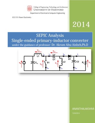
- 1. Department of Electrical & Computer Engineering ECE 573: Power Electronics ECE 573 power electronics SEPIC Analysis primary-inductor converter of professor: Dr. Akram Abu Single-ended primary under the guidance o 2014 Abu-Aisheh,Ph.D ANANTHALAKSHMI ADAPA 12/8/2014
- 2. Department of Electrical & Computer Engineering 1 Table of Contents SINGLE-ENDED PRIMARY-INDUCTOR CONVERTER 1. Abstract 2 2. overview 3 3. difference between converters 4 4. methodology 5 Continuous mode operation 6 5. practical design 7 Calculation considerations 7 Output voltage 8 L & C Voltages 8 Voltage Ripple 9 Diode current 9 MOSFET selection 10 Isolation 10 6. Results and Observation 11 LT Spice designing 11 7. disadvantages 13 8. refrences 13
- 3. Department of Electrical & Computer Engineering Abstract: The single-ended primary-inductance converter (SEPIC) is a DC/DC-converter that provides a positive regulated output voltage from an input voltage that varies from above to below the output voltage. This type of conversion is handy when the designer uses voltages (e.g.,12 V) from an unregulated input power supply such as a low-cost wall wart. Unfortunately, the SEPIC is difficult to understand and requires two inductors, making the power-supply footprint quite large. Recently, several inductor manufacturers began selling off-the-shelf coupled inductors in a single package at a cost only slightly higher than that of the comparable single inductor. The coupled inductor not only provides a smaller footprint but also, to get the same inductor ripple current, requires only half the inductance required for a SEPIC with two separate inductors. This article explains how to design a SEPIC converter with a coupled inductor. 2
- 4. Department of Electrical & Computer Engineering 3 Overview: Single-ended primary-inductor converter (SEPIC) is a type of DC-DC converter allowing the electrical potential (voltage) at its output to be greater than, less than, or equal to that at its input; the output of the SEPIC is controlled by the duty cycle of the control transistor. A SEPIC is essentially a boost converter followed by a buck-boost converter, therefore it is similar to a traditional buck-boost converter, but has advantages of having non-inverted output (the output has the same voltage polarity as the input), using a series capacitor to couple energy from the input to the output (and thus can respond more gracefully to a short-circuit output), and being capable of true shutdown: when the switch is turned off, its output drops to 0 V, following a fairly hefty transient dump of charge. SEPICs are useful in applications in which a battery voltage can be above and below that of the regulator's intended output. For example, a single lithium ion battery typically discharges from 4.2 volts to 3 volts; if other components require 3.3 volts, then the SEPIC would be effective.
- 5. Department of Electrical & Computer Engineering Different converters showing line current waveform, DCM self-PFC and power level 4
- 6. Department of Electrical & Computer Engineering 5 Methodology A converter similar to the Cuk is the single-ended primary inductance converter (SEPIC), as shown in Fig. below. The SEPIC can produce an output voltage that is either greater or less than the input but with no polarity reversal. To derive the relationship between input and output voltages, these initial assumptions are made: 1. Both inductors are very large and the currents in them are constant. 2. Both capacitors are very large and the voltages across them are constant. 3. The circuit is operating in the steady state, meaning that voltage and current waveforms are periodic. 4. For a duty ratio of D, the switch is closed for time DT and open for (1 _ D)T. 5. The switch and the diode are ideal.
- 7. Department of Electrical & Computer Engineering 6 Continuous mode action: A SEPIC is said to be in continuous-conduction mode ("continuous mode") if the current through the inductor L1 never falls to zero. During a SEPIC's steady-state operation, the average voltage across capacitor C1 (VC1) is equal to the input voltage (Vin). Because capacitor C1 blocks direct current (DC), the average current across it (IC1) is zero, making inductor L2 the only source of load current. Therefore, the average current through inductor L2 (IL2) is the same as the average load current and hence independent of the input voltage When switch turned on: When switch S1 is turned on, current IL1 increases and the current IL2 increases in the negative direction. (Mathematically, it decreases due to arrow direction.) The energy to increase the current IL1 comes from the input source. Since S1 is a short while closed, and the instantaneous voltage VC1 is approximately VIN, the voltage VL2 is approximately −VIN. Therefore, the capacitor C1 supplies the energy to increase the magnitude of the current in IL2 and thus increase the energy stored in L2. The easiest way to visualize this is to consider the bias voltages of the circuit in a d.c. state, then close S1. When switch turn off When switch S1 is turned off, the current IC1 becomes the same as the current IL1, since inductors do not allow instantaneous changes in current. The current IL2 will continue in the negative direction, in fact it never reverses direction. It can be seen from the diagram that a negative IL2 will add to the current IL1 to increase the current delivered to the load. Using Kirchhoff's Current Law, it can be shown that ID1 = IC1 - IL2. It can then be concluded, that while S1 is off, power is delivered to the load from both L2 and L1. C1, however is being charged by L1 during this off cycle, and will in turn recharge L2 during the on cycle.
- 8. Department of Electrical & Computer Engineering 7 The practical design Calculations By considering Vin = 12V D = 0.6 Fs = 200KHz L1 = L2 = 3.36μH
- 9. Department of Electrical & Computer Engineering C1 = C2 = 5.26μF I0 = 5A output voltage the output voltage can be determined using the formula below 8 ݒ0 = ܸ௦ ൬ ܦ 1 − ܦ ൰ = 12 ൬ Ͳ.6 1 − Ͳ.6 ൰ = 18ܸ L and C voltages: average inductor current, which is also the average source current will be calculated for calculating L and C values The average current in L1 is determined from ܫଵ = ܸ0 × ܫ0 ܸ௦ = 18 × 5 12 = 7.5ܣ Now Δ݅ଶ = Δ݅ଵ = ܸ௦ × ܦ ܮଵ × ܨ = 12 × Ͳ.6 3.36 × 1Ͳି × 2ͲͲ,ͲͲͲ = 1Ͳ.72ܣ Resulting the maximum and minimum current magnitudes in L1 are ܫଵ,௫ = ܫଵ + Δ݅ଵ 2 = 7.5 + ൬ 1Ͳ.72 2 ൰ = 12.86ܣ ܫଵ, = ܫଵ − Δ݅ଶ 2 = 7.5 − 1Ͳ.72 2 = 2.14 ܣ For the current in L2, the average is the same as the output current Io = 5 A. The variation in IL2 is determined ܫଶ,௫ = 5 + 1Ͳ.72 2 = 7.144ܣ ܫଶ, = 5 − 1Ͳ.72 2 = 2.86ܣ The variation in iL1 when the switch is closed is found from
- 10. Department of Electrical & Computer Engineering 9 ܸଵ = ܸଶ = ܸ௦ = ܮଵ ൬ Δ݅ଵ ܦܶ ൰ = 3.36 × 1Ͳି ൬ 1Ͳ.72 × 2ͲͲ,ͲͲͲ Ͳ.6 ൰ = 12ܸ The output stage consisting of the diode, C2, and the load resistor is the same as in the boost converter, so the output ripple voltage is ܸଶ = ܸଵ = ܸ௦ = 12ܸ Voltage Ripple: Kirchhoff’s voltage law applied to the circuit assuming no voltage ripple across the capacitors, shows that the voltage across the switch when it is open is Vs + Vo. the maximum reverse bias voltage across the diode when it is off is also Vs+ Vo. The output stage consisting of the diode, C2, and the load resistor is the same as in the boost converter, so the output ripple voltage is By calculating మ ೄோ = 3.6Ω ܴ = బ Δܸ0 = Δܸଶ = బ× ோమி = ଵ଼×0. ଷ.×ହ.ଶ×ଶ00,000 = 2.85ܸ Diode current Applications of Kirchhoff’s current law show that the diode and switch currents are iD = 7.5 +10 = 17.5A when switch open iD = 0 when switch closed and isw = 0 when switch open isw = 17.5A when switch closed
- 11. Department of Electrical & Computer Engineering ଶ × ܴௌ, × ܦெ௫ ൯ + (ܸௌ + ܸ0) × ܫொଵ × ൬ 10 and switch voltage stress can be calculated as ܸௌௐ,ௌாூ = ܸ௦ 1 − ܦ = 12 1 − Ͳ.6 = 3Ͳ Power MOSFET The MOSFET peak current is ܫொଵ,௫ = ܫଵ,௫ + ܫଶ,௫ = 12.86 + 7.84 = 2Ͳ.7ܣ and the RMS current is by considering VD = 0.5 ܫொଵ,௦ = ܫ0 ቌඨ (ܸ + ܸ௦ + ܸ) × (ܸ0 + ܸ) ଶ ቍ = 2.916ܣ ܸ௦ The rated drain voltage for the MOSFET must be higher than VIN+VOUT. RDS(ON) = 8 mΩ and QGD = 10 nC is selected in this design. The gate drive current IG is taken 0.3A. The estimated power loss is: ܲொଵ = ൫ ܫொଵ ܳீ × ܨ ܫீ ൰ = 44.78ܹ Isolation: Taking Isolated Single Ended Primary Inductance converters (Isolated SEPIC) are good choice that can be used in high step-up photovoltaic applications. This type of converters has advantages such as: 1- same input and output voltage polarity, 2- low input current ripple, 3- Possibility of having multiple outputs, 4- Possibility of working in both step-up and step-down modes, 5- Low amount of EMI due to low input current ripple and 6-Electrical isolation between input and output Simulation of SEPIC
- 12. Department of Electrical & Computer Engineering 11
- 13. Department of Electrical & Computer Engineering 12
- 14. Department of Electrical & Computer Engineering 13 Disadvantages: 1. Like buck–boost converters, SEPICs have a pulsating output current. The similar Cuk converter does not have this disadvantage, but it can only have negative output polarity, unless the isolated Cuk converter is used. 2. Since the SEPIC converter transfers all its energy via the series capacitor, a capacitor with high capacitance and current handling capability is required. 3. The fourth-order nature of the converter also makes the SEPIC converter difficult to control, making them only suitable for very slow varying applications. References: 1. Power Electronics text book by Daniel W. Hart 2. http://en.wikipedia.org/wiki/Single-ended_primary-inductor_converter 3. analysis of a SEPIC by Texas Instruments 4. high performance DC-DC controllers by liner technology 5. Analyzing the Sepic Converter by Dr. Ray Ridley, Ridley Engineering 6. Fundamentals of Power Electronics By Robert W. Erickson, Dragan Maksimovic