SlideShare une entreprise Scribd logo
1  sur  20
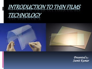
INTRODUCTIONTO THINFILMS
TECHNOLOGY
Presented by :
Sumit Kumar
Thin Films ???
 Thin films are just a layer of materials, thickness ranging
between (10-500) nanometers
 If there is no substrate then it is a “foil”.
fig: Zno thin film deposited on a substrate
Why Thin Films ???
 Maintain surface uniformity
 Simple fabrication
 Manufacturing requires less material
 Reduce light absorbing material
 Strange electrical, optical and mechanical properties
• Nowadays thin film technology used in many applications,
including microelectronics, optics, magnetic, hard resistant
coatings, micro-mechanics, etc.
• Better results in these areas depend on selective and
controlled deposition.
• There are a vast number of deposition methods available, all
methods have their specific advantages as well as
disadvantages based on substrate and source material,
thickness of deposited film.
• This makes it difficult to select the best technique for any
specific application. Some of these methods are discussed.
Technology Focus
Deposition Techniques
 Glow Discharge Processes
1. Sputtering
2. Plasma processes
 Gas phase chemical processes
1. Low Pressure CVD
2. Metal Organic CVD
3. Laser induced CVD
 Liquid Phase Chemical Processes
1. Electroplating
2. Spin on Techniques
.
• Vacuum evaporation Techniques
1. Convential Vacuum Evaporation
2. Molecular Beam evaporation
3. Molecular Beam Epitaxy
4. Reaction Evaporation
.Deposition based on Physical or
Chemical Processes
Deposition
Techniques
PhysicalVapor
Deposition
Vacuum
Evaporation
Techniques
Sputtering Spin Coatings
Chemical
Vapor
Deposition
Electroplating PECVD LPCVD
Plasma Enhanced CVD
.
• Lower Temperature Process
due to Plasma Enhancement
• Dissociation of precursor gas
molecules (Homogeneous
reactions)
• Ions bombard surface
making it more reactive
• Higher rates of deposition
are possible than with
LPCVD
Low Pressure CVD
 .
• Surface reaction limited
at low pressure
• Chamber may also be
heated or unheated
• Low pressure
environment increases
mean free path
• Better Step Coverage
and conformality than
APCVD
Electroplating
Sputtering
• It is basically an etching process which was first discovered in
1892 and developed as a thin film deposition techniques in
1920 by Langmuir.
Spin Coating
Evaporation Deposition
The material is heated in high vacuum chamber (P < 10-5 Torr)
to minimize the collision in source atoms, it is also called
Vacuum Deposition.
Heating is done by resistive or e-beam sources.
Surface interactions are physical, can be very fast (>1m/min
possible)
High sticking coefficient leading to poor conformal
coverage/significant shadow. But this also makes evaporation
the most popular thin film deposition for nanofabrication using
liftoff process.
Deposition rate is determined by emitted flux and by geometry
of the source and wafer.
Evaporation is not widely used by industry as sputter
13
 Evaporator based on heating process
1. Thermal Evaporator(Resistive heating)
2. Electron beam Evaporator(Heating by electron beam)
3. Inductive Evaporator (Inductive heating – most unpopular
one)
Thermal Evaporator
 Used for material whose vapor pressure can be reasonable at
(1600-1800)°C or less than that. Common evaporant materials
are Au, Ag, Al, Sn, Cds, Pbs, Cdse etc.
 Thermal Evaporator
1. Simple, used at large scale
2. W, Ta filaments are used as heaters.
3. Filament produces current to (200-300) ampere.
4. Substrate exposes to Infrared or Visible rays
5. Contamination from heated boat
 E-Beam Evaporator
1. More complex and can be used for almost all kind of
materials .
2. Less contamination and heating to wafer.
3. Exposes substrate to secondary electron radiation
4. X-Ray can be generated by high voltage electron beam.
As it produces X-ray beams so it can’t be used for
MOSFET(X-ray may damage substrate as well as dielectrics)
Issues with Evaporation System
 Step Coverage
 Alloy Evaporation
 Shadow Evaporation
Types of Thin Films
 Si based thin films
 CdTe Thin Films
 CIGS Thin Films
 CZTS Thin Films
Applications
• Microelectronics - electrical conductors, electrical barriers,
diffusion barriers.
• Magnetic sensors - sense I, B or changes in them
• Gas sensors, SAW devices.
• Tailored materials - layer very thin films to develop materials with
new properties
• Optics- anti-reflection coatings
• Corrosion protection
• Wear resistance
Thank You

Contenu connexe

Tendances

Pulsed Laser Ablation
Pulsed Laser AblationPulsed Laser Ablation
Pulsed Laser AblationArun Aravind
 
Pulse laser deposition of thin film
Pulse laser deposition of thin filmPulse laser deposition of thin film
Pulse laser deposition of thin filmUOG PHYSICISTS !!!!!
 
CVD AND PVD THIN FILM TECHNIQUES
CVD AND PVD THIN FILM TECHNIQUESCVD AND PVD THIN FILM TECHNIQUES
CVD AND PVD THIN FILM TECHNIQUESHHV SOLAR Pvt Ltd
 
Physical Vapour Deposition (PVD)
Physical Vapour Deposition (PVD)Physical Vapour Deposition (PVD)
Physical Vapour Deposition (PVD)jitendrahemwani
 
Molecular Beam Epitaxy-MBE---ABU SYED KUET
Molecular Beam Epitaxy-MBE---ABU SYED KUETMolecular Beam Epitaxy-MBE---ABU SYED KUET
Molecular Beam Epitaxy-MBE---ABU SYED KUETA. S. M. Jannatul Islam
 
METAL ORGANIC CHEMICAL VAPOR DEPOSITION- MOCVD--ABU SYED KUET
METAL ORGANIC CHEMICAL VAPOR DEPOSITION- MOCVD--ABU SYED KUETMETAL ORGANIC CHEMICAL VAPOR DEPOSITION- MOCVD--ABU SYED KUET
METAL ORGANIC CHEMICAL VAPOR DEPOSITION- MOCVD--ABU SYED KUETA. S. M. Jannatul Islam
 
Epitaxy techniques
Epitaxy techniquesEpitaxy techniques
Epitaxy techniquescherukurir
 
Chemical vapor deposition (cvd)
Chemical vapor deposition (cvd)Chemical vapor deposition (cvd)
Chemical vapor deposition (cvd)Khalid Raza
 
6.a.preparation of thin films
6.a.preparation of thin films6.a.preparation of thin films
6.a.preparation of thin filmsNarayan Behera
 
Vacuum Science and Technology for Thin Film Device Processing
Vacuum Science and Technology for Thin Film Device ProcessingVacuum Science and Technology for Thin Film Device Processing
Vacuum Science and Technology for Thin Film Device Processingcdtpv
 
Sputtering process and its types
Sputtering process and its typesSputtering process and its types
Sputtering process and its typesMuhammadWajid37
 
Thin film and thick film resistor
Thin film and thick film resistorThin film and thick film resistor
Thin film and thick film resistorbiruk gedif
 
Epitaxial Crystal Growth: Methods & Analysis
Epitaxial Crystal Growth: Methods & Analysis Epitaxial Crystal Growth: Methods & Analysis
Epitaxial Crystal Growth: Methods & Analysis KaŃnán RãjËev
 

Tendances (20)

Chemical vapour deposition
Chemical vapour depositionChemical vapour deposition
Chemical vapour deposition
 
Pulsed Laser Ablation
Pulsed Laser AblationPulsed Laser Ablation
Pulsed Laser Ablation
 
Apps of thin films
Apps of thin filmsApps of thin films
Apps of thin films
 
Pulse laser deposition of thin film
Pulse laser deposition of thin filmPulse laser deposition of thin film
Pulse laser deposition of thin film
 
CVD AND PVD THIN FILM TECHNIQUES
CVD AND PVD THIN FILM TECHNIQUESCVD AND PVD THIN FILM TECHNIQUES
CVD AND PVD THIN FILM TECHNIQUES
 
Physical Vapour Deposition (PVD)
Physical Vapour Deposition (PVD)Physical Vapour Deposition (PVD)
Physical Vapour Deposition (PVD)
 
Magnetron sputtering
Magnetron sputteringMagnetron sputtering
Magnetron sputtering
 
Molecular Beam Epitaxy-MBE---ABU SYED KUET
Molecular Beam Epitaxy-MBE---ABU SYED KUETMolecular Beam Epitaxy-MBE---ABU SYED KUET
Molecular Beam Epitaxy-MBE---ABU SYED KUET
 
METAL ORGANIC CHEMICAL VAPOR DEPOSITION- MOCVD--ABU SYED KUET
METAL ORGANIC CHEMICAL VAPOR DEPOSITION- MOCVD--ABU SYED KUETMETAL ORGANIC CHEMICAL VAPOR DEPOSITION- MOCVD--ABU SYED KUET
METAL ORGANIC CHEMICAL VAPOR DEPOSITION- MOCVD--ABU SYED KUET
 
Rani
RaniRani
Rani
 
Epitaxy techniques
Epitaxy techniquesEpitaxy techniques
Epitaxy techniques
 
Chemical vapor deposition (cvd)
Chemical vapor deposition (cvd)Chemical vapor deposition (cvd)
Chemical vapor deposition (cvd)
 
6.a.preparation of thin films
6.a.preparation of thin films6.a.preparation of thin films
6.a.preparation of thin films
 
Vacuum Science and Technology for Thin Film Device Processing
Vacuum Science and Technology for Thin Film Device ProcessingVacuum Science and Technology for Thin Film Device Processing
Vacuum Science and Technology for Thin Film Device Processing
 
Physical Vapour Deposition
Physical Vapour DepositionPhysical Vapour Deposition
Physical Vapour Deposition
 
Cvd
CvdCvd
Cvd
 
Sputtering process and its types
Sputtering process and its typesSputtering process and its types
Sputtering process and its types
 
Apps of thin films
Apps of thin filmsApps of thin films
Apps of thin films
 
Thin film and thick film resistor
Thin film and thick film resistorThin film and thick film resistor
Thin film and thick film resistor
 
Epitaxial Crystal Growth: Methods & Analysis
Epitaxial Crystal Growth: Methods & Analysis Epitaxial Crystal Growth: Methods & Analysis
Epitaxial Crystal Growth: Methods & Analysis
 

Similaire à why and how thin films

anti reflective coatings on the solar photo voltaic panel's
anti reflective coatings on the solar photo voltaic panel'santi reflective coatings on the solar photo voltaic panel's
anti reflective coatings on the solar photo voltaic panel'sRajneesh Gautam
 
composites applications in electrical and electronics
composites applications in electrical and electronicscomposites applications in electrical and electronics
composites applications in electrical and electronicsgirish_raghunathan4488
 
Composites in electrical and electronic applications
Composites in electrical and electronic applicationsComposites in electrical and electronic applications
Composites in electrical and electronic applicationsgirish_raghunathan4488
 
The Evolution Of An Electronic Material
The Evolution Of An Electronic MaterialThe Evolution Of An Electronic Material
The Evolution Of An Electronic Materialdavekellerman
 
The Evolution Of An Electronic Material
The Evolution Of An Electronic MaterialThe Evolution Of An Electronic Material
The Evolution Of An Electronic Materialgueste2531
 
ETE444-lec5-micro-fabrication.pptx
ETE444-lec5-micro-fabrication.pptxETE444-lec5-micro-fabrication.pptx
ETE444-lec5-micro-fabrication.pptxmashiur
 
ETE444-lec5-micro-fabrication.pptx
ETE444-lec5-micro-fabrication.pptxETE444-lec5-micro-fabrication.pptx
ETE444-lec5-micro-fabrication.pptxmashiur
 
MSE PhD lecture. Adv. Mater. Synthesis. Thin Films. Oct 23, 2014.
MSE PhD lecture. Adv. Mater. Synthesis. Thin Films. Oct 23, 2014.MSE PhD lecture. Adv. Mater. Synthesis. Thin Films. Oct 23, 2014.
MSE PhD lecture. Adv. Mater. Synthesis. Thin Films. Oct 23, 2014.Toru Hara
 
Mse phd lecture
Mse phd lectureMse phd lecture
Mse phd lectureToru Hara
 
ETE444-lec5-micro-fabrication.pdf
ETE444-lec5-micro-fabrication.pdfETE444-lec5-micro-fabrication.pdf
ETE444-lec5-micro-fabrication.pdfmashiur
 
ETE444-lec5-micro-fabrication.pdf
ETE444-lec5-micro-fabrication.pdfETE444-lec5-micro-fabrication.pdf
ETE444-lec5-micro-fabrication.pdfmashiur
 
Rosa alejandra lukaszew a review of the thin film techniques potentially ap...
Rosa alejandra lukaszew   a review of the thin film techniques potentially ap...Rosa alejandra lukaszew   a review of the thin film techniques potentially ap...
Rosa alejandra lukaszew a review of the thin film techniques potentially ap...thinfilmsworkshop
 
09sputterdeposition.ppt
09sputterdeposition.ppt09sputterdeposition.ppt
09sputterdeposition.pptDevendraBhale
 
Advanced_Coating.pptx
Advanced_Coating.pptxAdvanced_Coating.pptx
Advanced_Coating.pptxJiaJunWang17
 

Similaire à why and how thin films (20)

anti reflective coatings on the solar photo voltaic panel's
anti reflective coatings on the solar photo voltaic panel'santi reflective coatings on the solar photo voltaic panel's
anti reflective coatings on the solar photo voltaic panel's
 
Applications of nanomaterials by dr.ck
Applications of nanomaterials by dr.ckApplications of nanomaterials by dr.ck
Applications of nanomaterials by dr.ck
 
PVD.ppt
PVD.pptPVD.ppt
PVD.ppt
 
PPT 2.ppt
PPT 2.pptPPT 2.ppt
PPT 2.ppt
 
Nano materials
Nano materialsNano materials
Nano materials
 
Ldb Convergenze Parallele_07
Ldb Convergenze Parallele_07Ldb Convergenze Parallele_07
Ldb Convergenze Parallele_07
 
composites applications in electrical and electronics
composites applications in electrical and electronicscomposites applications in electrical and electronics
composites applications in electrical and electronics
 
Composites in electrical and electronic applications
Composites in electrical and electronic applicationsComposites in electrical and electronic applications
Composites in electrical and electronic applications
 
The Evolution Of An Electronic Material
The Evolution Of An Electronic MaterialThe Evolution Of An Electronic Material
The Evolution Of An Electronic Material
 
The Evolution Of An Electronic Material
The Evolution Of An Electronic MaterialThe Evolution Of An Electronic Material
The Evolution Of An Electronic Material
 
ETE444-lec5-micro-fabrication.pptx
ETE444-lec5-micro-fabrication.pptxETE444-lec5-micro-fabrication.pptx
ETE444-lec5-micro-fabrication.pptx
 
ETE444-lec5-micro-fabrication.pptx
ETE444-lec5-micro-fabrication.pptxETE444-lec5-micro-fabrication.pptx
ETE444-lec5-micro-fabrication.pptx
 
MSE PhD lecture. Adv. Mater. Synthesis. Thin Films. Oct 23, 2014.
MSE PhD lecture. Adv. Mater. Synthesis. Thin Films. Oct 23, 2014.MSE PhD lecture. Adv. Mater. Synthesis. Thin Films. Oct 23, 2014.
MSE PhD lecture. Adv. Mater. Synthesis. Thin Films. Oct 23, 2014.
 
Mse phd lecture
Mse phd lectureMse phd lecture
Mse phd lecture
 
ETE444-lec5-micro-fabrication.pdf
ETE444-lec5-micro-fabrication.pdfETE444-lec5-micro-fabrication.pdf
ETE444-lec5-micro-fabrication.pdf
 
ETE444-lec5-micro-fabrication.pdf
ETE444-lec5-micro-fabrication.pdfETE444-lec5-micro-fabrication.pdf
ETE444-lec5-micro-fabrication.pdf
 
Rosa alejandra lukaszew a review of the thin film techniques potentially ap...
Rosa alejandra lukaszew   a review of the thin film techniques potentially ap...Rosa alejandra lukaszew   a review of the thin film techniques potentially ap...
Rosa alejandra lukaszew a review of the thin film techniques potentially ap...
 
Rosa alejandra lukaszew a review of the thin film techniques potentially ap...
Rosa alejandra lukaszew   a review of the thin film techniques potentially ap...Rosa alejandra lukaszew   a review of the thin film techniques potentially ap...
Rosa alejandra lukaszew a review of the thin film techniques potentially ap...
 
09sputterdeposition.ppt
09sputterdeposition.ppt09sputterdeposition.ppt
09sputterdeposition.ppt
 
Advanced_Coating.pptx
Advanced_Coating.pptxAdvanced_Coating.pptx
Advanced_Coating.pptx
 

Dernier

Understanding Accommodations and Modifications
Understanding  Accommodations and ModificationsUnderstanding  Accommodations and Modifications
Understanding Accommodations and ModificationsMJDuyan
 
ICT role in 21st century education and it's challenges.
ICT role in 21st century education and it's challenges.ICT role in 21st century education and it's challenges.
ICT role in 21st century education and it's challenges.MaryamAhmad92
 
Explore beautiful and ugly buildings. Mathematics helps us create beautiful d...
Explore beautiful and ugly buildings. Mathematics helps us create beautiful d...Explore beautiful and ugly buildings. Mathematics helps us create beautiful d...
Explore beautiful and ugly buildings. Mathematics helps us create beautiful d...christianmathematics
 
Kodo Millet PPT made by Ghanshyam bairwa college of Agriculture kumher bhara...
Kodo Millet  PPT made by Ghanshyam bairwa college of Agriculture kumher bhara...Kodo Millet  PPT made by Ghanshyam bairwa college of Agriculture kumher bhara...
Kodo Millet PPT made by Ghanshyam bairwa college of Agriculture kumher bhara...pradhanghanshyam7136
 
Making communications land - Are they received and understood as intended? we...
Making communications land - Are they received and understood as intended? we...Making communications land - Are they received and understood as intended? we...
Making communications land - Are they received and understood as intended? we...Association for Project Management
 
TỔNG ÔN TẬP THI VÀO LỚP 10 MÔN TIẾNG ANH NĂM HỌC 2023 - 2024 CÓ ĐÁP ÁN (NGỮ Â...
TỔNG ÔN TẬP THI VÀO LỚP 10 MÔN TIẾNG ANH NĂM HỌC 2023 - 2024 CÓ ĐÁP ÁN (NGỮ Â...TỔNG ÔN TẬP THI VÀO LỚP 10 MÔN TIẾNG ANH NĂM HỌC 2023 - 2024 CÓ ĐÁP ÁN (NGỮ Â...
TỔNG ÔN TẬP THI VÀO LỚP 10 MÔN TIẾNG ANH NĂM HỌC 2023 - 2024 CÓ ĐÁP ÁN (NGỮ Â...Nguyen Thanh Tu Collection
 
Activity 01 - Artificial Culture (1).pdf
Activity 01 - Artificial Culture (1).pdfActivity 01 - Artificial Culture (1).pdf
Activity 01 - Artificial Culture (1).pdfciinovamais
 
HMCS Max Bernays Pre-Deployment Brief (May 2024).pptx
HMCS Max Bernays Pre-Deployment Brief (May 2024).pptxHMCS Max Bernays Pre-Deployment Brief (May 2024).pptx
HMCS Max Bernays Pre-Deployment Brief (May 2024).pptxEsquimalt MFRC
 
Mixin Classes in Odoo 17 How to Extend Models Using Mixin Classes
Mixin Classes in Odoo 17  How to Extend Models Using Mixin ClassesMixin Classes in Odoo 17  How to Extend Models Using Mixin Classes
Mixin Classes in Odoo 17 How to Extend Models Using Mixin ClassesCeline George
 
Towards a code of practice for AI in AT.pptx
Towards a code of practice for AI in AT.pptxTowards a code of practice for AI in AT.pptx
Towards a code of practice for AI in AT.pptxJisc
 
Python Notes for mca i year students osmania university.docx
Python Notes for mca i year students osmania university.docxPython Notes for mca i year students osmania university.docx
Python Notes for mca i year students osmania university.docxRamakrishna Reddy Bijjam
 
2024-NATIONAL-LEARNING-CAMP-AND-OTHER.pptx
2024-NATIONAL-LEARNING-CAMP-AND-OTHER.pptx2024-NATIONAL-LEARNING-CAMP-AND-OTHER.pptx
2024-NATIONAL-LEARNING-CAMP-AND-OTHER.pptxMaritesTamaniVerdade
 
Graduate Outcomes Presentation Slides - English
Graduate Outcomes Presentation Slides - EnglishGraduate Outcomes Presentation Slides - English
Graduate Outcomes Presentation Slides - Englishneillewis46
 
FSB Advising Checklist - Orientation 2024
FSB Advising Checklist - Orientation 2024FSB Advising Checklist - Orientation 2024
FSB Advising Checklist - Orientation 2024Elizabeth Walsh
 
Introduction to Nonprofit Accounting: The Basics
Introduction to Nonprofit Accounting: The BasicsIntroduction to Nonprofit Accounting: The Basics
Introduction to Nonprofit Accounting: The BasicsTechSoup
 
SKILL OF INTRODUCING THE LESSON MICRO SKILLS.pptx
SKILL OF INTRODUCING THE LESSON MICRO SKILLS.pptxSKILL OF INTRODUCING THE LESSON MICRO SKILLS.pptx
SKILL OF INTRODUCING THE LESSON MICRO SKILLS.pptxAmanpreet Kaur
 
1029 - Danh muc Sach Giao Khoa 10 . pdf
1029 -  Danh muc Sach Giao Khoa 10 . pdf1029 -  Danh muc Sach Giao Khoa 10 . pdf
1029 - Danh muc Sach Giao Khoa 10 . pdfQucHHunhnh
 
Basic Civil Engineering first year Notes- Chapter 4 Building.pptx
Basic Civil Engineering first year Notes- Chapter 4 Building.pptxBasic Civil Engineering first year Notes- Chapter 4 Building.pptx
Basic Civil Engineering first year Notes- Chapter 4 Building.pptxDenish Jangid
 
Food safety_Challenges food safety laboratories_.pdf
Food safety_Challenges food safety laboratories_.pdfFood safety_Challenges food safety laboratories_.pdf
Food safety_Challenges food safety laboratories_.pdfSherif Taha
 

Dernier (20)

Understanding Accommodations and Modifications
Understanding  Accommodations and ModificationsUnderstanding  Accommodations and Modifications
Understanding Accommodations and Modifications
 
ICT role in 21st century education and it's challenges.
ICT role in 21st century education and it's challenges.ICT role in 21st century education and it's challenges.
ICT role in 21st century education and it's challenges.
 
Explore beautiful and ugly buildings. Mathematics helps us create beautiful d...
Explore beautiful and ugly buildings. Mathematics helps us create beautiful d...Explore beautiful and ugly buildings. Mathematics helps us create beautiful d...
Explore beautiful and ugly buildings. Mathematics helps us create beautiful d...
 
Kodo Millet PPT made by Ghanshyam bairwa college of Agriculture kumher bhara...
Kodo Millet  PPT made by Ghanshyam bairwa college of Agriculture kumher bhara...Kodo Millet  PPT made by Ghanshyam bairwa college of Agriculture kumher bhara...
Kodo Millet PPT made by Ghanshyam bairwa college of Agriculture kumher bhara...
 
Making communications land - Are they received and understood as intended? we...
Making communications land - Are they received and understood as intended? we...Making communications land - Are they received and understood as intended? we...
Making communications land - Are they received and understood as intended? we...
 
TỔNG ÔN TẬP THI VÀO LỚP 10 MÔN TIẾNG ANH NĂM HỌC 2023 - 2024 CÓ ĐÁP ÁN (NGỮ Â...
TỔNG ÔN TẬP THI VÀO LỚP 10 MÔN TIẾNG ANH NĂM HỌC 2023 - 2024 CÓ ĐÁP ÁN (NGỮ Â...TỔNG ÔN TẬP THI VÀO LỚP 10 MÔN TIẾNG ANH NĂM HỌC 2023 - 2024 CÓ ĐÁP ÁN (NGỮ Â...
TỔNG ÔN TẬP THI VÀO LỚP 10 MÔN TIẾNG ANH NĂM HỌC 2023 - 2024 CÓ ĐÁP ÁN (NGỮ Â...
 
Activity 01 - Artificial Culture (1).pdf
Activity 01 - Artificial Culture (1).pdfActivity 01 - Artificial Culture (1).pdf
Activity 01 - Artificial Culture (1).pdf
 
HMCS Max Bernays Pre-Deployment Brief (May 2024).pptx
HMCS Max Bernays Pre-Deployment Brief (May 2024).pptxHMCS Max Bernays Pre-Deployment Brief (May 2024).pptx
HMCS Max Bernays Pre-Deployment Brief (May 2024).pptx
 
Mixin Classes in Odoo 17 How to Extend Models Using Mixin Classes
Mixin Classes in Odoo 17  How to Extend Models Using Mixin ClassesMixin Classes in Odoo 17  How to Extend Models Using Mixin Classes
Mixin Classes in Odoo 17 How to Extend Models Using Mixin Classes
 
Towards a code of practice for AI in AT.pptx
Towards a code of practice for AI in AT.pptxTowards a code of practice for AI in AT.pptx
Towards a code of practice for AI in AT.pptx
 
Python Notes for mca i year students osmania university.docx
Python Notes for mca i year students osmania university.docxPython Notes for mca i year students osmania university.docx
Python Notes for mca i year students osmania university.docx
 
2024-NATIONAL-LEARNING-CAMP-AND-OTHER.pptx
2024-NATIONAL-LEARNING-CAMP-AND-OTHER.pptx2024-NATIONAL-LEARNING-CAMP-AND-OTHER.pptx
2024-NATIONAL-LEARNING-CAMP-AND-OTHER.pptx
 
Graduate Outcomes Presentation Slides - English
Graduate Outcomes Presentation Slides - EnglishGraduate Outcomes Presentation Slides - English
Graduate Outcomes Presentation Slides - English
 
FSB Advising Checklist - Orientation 2024
FSB Advising Checklist - Orientation 2024FSB Advising Checklist - Orientation 2024
FSB Advising Checklist - Orientation 2024
 
Introduction to Nonprofit Accounting: The Basics
Introduction to Nonprofit Accounting: The BasicsIntroduction to Nonprofit Accounting: The Basics
Introduction to Nonprofit Accounting: The Basics
 
Spatium Project Simulation student brief
Spatium Project Simulation student briefSpatium Project Simulation student brief
Spatium Project Simulation student brief
 
SKILL OF INTRODUCING THE LESSON MICRO SKILLS.pptx
SKILL OF INTRODUCING THE LESSON MICRO SKILLS.pptxSKILL OF INTRODUCING THE LESSON MICRO SKILLS.pptx
SKILL OF INTRODUCING THE LESSON MICRO SKILLS.pptx
 
1029 - Danh muc Sach Giao Khoa 10 . pdf
1029 -  Danh muc Sach Giao Khoa 10 . pdf1029 -  Danh muc Sach Giao Khoa 10 . pdf
1029 - Danh muc Sach Giao Khoa 10 . pdf
 
Basic Civil Engineering first year Notes- Chapter 4 Building.pptx
Basic Civil Engineering first year Notes- Chapter 4 Building.pptxBasic Civil Engineering first year Notes- Chapter 4 Building.pptx
Basic Civil Engineering first year Notes- Chapter 4 Building.pptx
 
Food safety_Challenges food safety laboratories_.pdf
Food safety_Challenges food safety laboratories_.pdfFood safety_Challenges food safety laboratories_.pdf
Food safety_Challenges food safety laboratories_.pdf
 

why and how thin films

  • 2. Thin Films ???  Thin films are just a layer of materials, thickness ranging between (10-500) nanometers  If there is no substrate then it is a “foil”. fig: Zno thin film deposited on a substrate
  • 3. Why Thin Films ???  Maintain surface uniformity  Simple fabrication  Manufacturing requires less material  Reduce light absorbing material  Strange electrical, optical and mechanical properties
  • 4. • Nowadays thin film technology used in many applications, including microelectronics, optics, magnetic, hard resistant coatings, micro-mechanics, etc. • Better results in these areas depend on selective and controlled deposition. • There are a vast number of deposition methods available, all methods have their specific advantages as well as disadvantages based on substrate and source material, thickness of deposited film. • This makes it difficult to select the best technique for any specific application. Some of these methods are discussed. Technology Focus
  • 5. Deposition Techniques  Glow Discharge Processes 1. Sputtering 2. Plasma processes  Gas phase chemical processes 1. Low Pressure CVD 2. Metal Organic CVD 3. Laser induced CVD  Liquid Phase Chemical Processes 1. Electroplating 2. Spin on Techniques
  • 6. . • Vacuum evaporation Techniques 1. Convential Vacuum Evaporation 2. Molecular Beam evaporation 3. Molecular Beam Epitaxy 4. Reaction Evaporation
  • 7. .Deposition based on Physical or Chemical Processes Deposition Techniques PhysicalVapor Deposition Vacuum Evaporation Techniques Sputtering Spin Coatings Chemical Vapor Deposition Electroplating PECVD LPCVD
  • 8. Plasma Enhanced CVD . • Lower Temperature Process due to Plasma Enhancement • Dissociation of precursor gas molecules (Homogeneous reactions) • Ions bombard surface making it more reactive • Higher rates of deposition are possible than with LPCVD
  • 9. Low Pressure CVD  . • Surface reaction limited at low pressure • Chamber may also be heated or unheated • Low pressure environment increases mean free path • Better Step Coverage and conformality than APCVD
  • 11. Sputtering • It is basically an etching process which was first discovered in 1892 and developed as a thin film deposition techniques in 1920 by Langmuir.
  • 13. Evaporation Deposition The material is heated in high vacuum chamber (P < 10-5 Torr) to minimize the collision in source atoms, it is also called Vacuum Deposition. Heating is done by resistive or e-beam sources. Surface interactions are physical, can be very fast (>1m/min possible) High sticking coefficient leading to poor conformal coverage/significant shadow. But this also makes evaporation the most popular thin film deposition for nanofabrication using liftoff process. Deposition rate is determined by emitted flux and by geometry of the source and wafer. Evaporation is not widely used by industry as sputter 13
  • 14.  Evaporator based on heating process 1. Thermal Evaporator(Resistive heating) 2. Electron beam Evaporator(Heating by electron beam) 3. Inductive Evaporator (Inductive heating – most unpopular one)
  • 15. Thermal Evaporator  Used for material whose vapor pressure can be reasonable at (1600-1800)°C or less than that. Common evaporant materials are Au, Ag, Al, Sn, Cds, Pbs, Cdse etc.
  • 16.  Thermal Evaporator 1. Simple, used at large scale 2. W, Ta filaments are used as heaters. 3. Filament produces current to (200-300) ampere. 4. Substrate exposes to Infrared or Visible rays 5. Contamination from heated boat  E-Beam Evaporator 1. More complex and can be used for almost all kind of materials . 2. Less contamination and heating to wafer. 3. Exposes substrate to secondary electron radiation 4. X-Ray can be generated by high voltage electron beam. As it produces X-ray beams so it can’t be used for MOSFET(X-ray may damage substrate as well as dielectrics)
  • 17. Issues with Evaporation System  Step Coverage  Alloy Evaporation  Shadow Evaporation
  • 18. Types of Thin Films  Si based thin films  CdTe Thin Films  CIGS Thin Films  CZTS Thin Films
  • 19. Applications • Microelectronics - electrical conductors, electrical barriers, diffusion barriers. • Magnetic sensors - sense I, B or changes in them • Gas sensors, SAW devices. • Tailored materials - layer very thin films to develop materials with new properties • Optics- anti-reflection coatings • Corrosion protection • Wear resistance