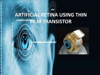
Artificial retina using thin film transistor technology
•Télécharger en tant que PPTX, PDF•
41 j'aime•9,691 vues

Use of TFT technology for retinal vision.

Recommandé
Contenu connexe
Tendances
Tendances (20)
Similaire à Artificial retina using thin film transistor technology
Similaire à Artificial retina using thin film transistor technology (20)
Plus de Venkata Raja Paruchuru
Plus de Venkata Raja Paruchuru (20)
Dernier
Dernier (20)
Artificial retina using thin film transistor technology
- 1. ARTIFICIAL RETINA USING THIN FILM TRANSISTOR
- 2. INTRODUCTION • The Artificial Retina made using Thin-Film Transistors, which can be fabricated on transparent and flexible substrates. • Electronic photo devices and circuits are integrated on the artificial retina. • Implanted on the inside surface of the living retina at the back part of the human eyeballs. Moreover, since the human eyeballs are curved, the flexible substrate is also preferable. • Wireless power supply is used
- 3. Retinal Implantation • A retinal implant is a biomedical implant technology • The first application of an implantable stimulator for vision restoration was developed by Drs. Brindley and Lewin in 1968. • There are two types of retinal implants namely epiretinal implant and subretinal implant.
- 4. Operation • It uses the same fabrication processes as conventional poly-Si TFTs and encapsulated using SiO2 • The retina array includes matrix-like multiple retina pixels • The retina pixel consists of a photo transistor, current mirror, and load resistance. • The photosensitivity of the reverse-biased p/i/n poly-Si phototransistor is 150 pA at 1000 lx for white light. • The retina pix-els irradiated with bright light output a higher Vout, whereas the retina pixels irradiated with darker light output a lower Vout.
- 5. Fabrication of thin film phototransistors • Low temperature poly-Si TFTs have been developed in order to fabricate active matrix LCDs with integrated drivers on large glass substrates. • For integrated drivers, CMOS configurations are indispensable. • Ion implantation is one of the key factors in fabricating
- 6. ION DOPING TECHNIC • The new I/D system which is one of the non mass separated implanters. 5 percent PH3 or 5 percent B2H6 diluted by hydrogen is used for the doping gas and an RF plasma is formed in the chamber by RF power with a frequency of 13.56MHz. Main features of this system are: 1) A large beam area (over 300 mm square) 2)A high accelerating voltage (maximum: 110 KeV)
- 7. Self Aligned structure and TFT characteristics • S/A TFTs and non-S/A TFTs with 25 nm thick as- deposited channel poly Si r31 were fabricated on the glass substrates. • The new I/D technique was used to achieve a self- aligned structure. • In these experiments, it is found that the characteristics of S/A and non-S/A TFTs are similar. • No degradation can be observed as a result of using the new I/D technique.
- 8. New Masking technique and CMOS Process • A non-resist-masking process, however, is required when the CMOS configuration is fabricated using the new I/D technique. • Since the temperature of the substrate reaches about 300oC due to the high accelerating voltage. • In order to solve this problem, a new masking technique is also proposed. • An SiO2 buffer layer is deposited on the glass substrate to protect TFTs from contamination from components of the glass.
- 9. Electro optical Measurement • The p/i/n TFPT is located on a rubber spacer in a shield chamber and connected via a manual prober to a voltage source and ampere meter.
- 10. WIRELESS POWER SUPPLY USING INDUCTIVE COUPLING • Many implanted electrical power to function; be it in the form of an im-planted battery or via wireless power transmission. • which requires additional surgery is undesirable. • An example of this is a retinal prosthesis. • continuous power transmission • Efficient transmission of power is a performance limiting factor • High density electrode array with more than 1000 electrodes will consume about 45 mW of power.
- 11. • Chip-25mw • Neuronal stimulation-20mw(3.3vth) • Based on 64 simultaneously operating electrodes each requiring a maximum of 0.3 mW at 60 Hz image refresh rate.
- 12. Disadvantages of power transmission • Difficulty in placing a large receive coil inside the eye. • We face are large separation between the coils • Reduction in power transfer to the device. Overcome problems: • Intermediate link between the primary and secondary coil • Which are embedded under the wall of the eye.
- 13. Working • The power transmitter consists of an ac voltage source(10V,34khz) and induction coil.
- 14. PIN • A PIN diode is a diode with a wide, undoped intrinsic semiconductor region between a p-type semiconductor and an n-type semiconductor region. The p-type and n-type regions are typically heavily doped because they are used for ohmic contacts. The wide intrinsic region is in contrast to an ordinary PNdiode.
- 15. CONCLUSIONS •The articial retina using poly-Si TFTs and wireless power supply using inductive couplinare located in a light-shield chamber •Vout in each retina pixel is probed by a manual prober and voltage meter. •it is driven using unstable power source generated by induc-tive coupling, Diode Bridge, and Zener diodes.
- 16. THANK YOU