SlideShare une entreprise Scribd logo
1  sur  9
Télécharger pour lire hors ligne
IOSR Journal of Electronics and Communication Engineering (IOSR-JECE)
e-ISSN: 2278-2834,p- ISSN: 2278-8735.Volume 10, Issue 1, Ver. 1 (Jan - Feb. 2015), PP 36-44
www.iosrjournals.org
DOI: 10.9790/2834-10113644 www.iosrjournals.org 36 | Page
Multiplier and Accumulator Using Csla
Asst Prof, Anoop M M
Electronics and Communication Engineering MG University College Of Engineering And
Technology,Thodupuzha
Abstract: With the recent rapid advances in multimedia and communication systems, real-time signal
processing like audio signal processing, video/image processing, or large-capacity data processing are
increasingly being demanded. The multiplier and multiplier-and-accumulator (MAC) are the essential
elements of the digital signal processing such as filtering, convolution, and Inner products.
Index Terms: Booth multiplier, carry save adder,Booth multiplier,Digital signal processing(DSP), multiplier
and-accumulator(MAC).
I. Introduction
A. Ripple Carry Adder
Multiple full adder circuits can be cascaded in parallel to add an N-bit number. For an N- bit parallel
adder, there must be N number of full adder circuits. A ripple carry adder is a logic circuit in which the carry-
out of each full adder is the carry in of the succeeding next most significant full adder. It is called a ripple carry
adder because each carry bit gets rippled into the next stage. In a ripple carry adder the sum and carry out bits
of any half adder stage is not valid until the carry in of that stage occurs. A propagation delay inside the logic
circuitry is the reason behind this. Propagation delay is time elapsed between the application of an input and
occurrence of the corresponding output. Consider a NOT gate, When the input is “0″ the output will be “1″ and
vice versa. The time taken for the NOT gate‟s output to become “0″ after the application of logic “1″ to the
NOT gate‟s input is the propagation delay here. Similarly the carry propagation delay is the time elapsed
between the application of the carry in signal and the occurrence of the carry out (Cout) signal. Circuit
diagram of a 4-bit ripple carry adder is shown below.
Fig. 3.1. Ripple carry adder
Sum out S0 and carry out Cout of the Full Adder 1 is valid only after the propagation delay of Full
Adder 1. In the same way, Sum out S3 of the Full Adder is valid only after the joint propagation delays of Full
Adder 1 to Full Adder 4. In simple words, the final result of the ripple carry adder is valid only after the joint
propagation delays of all full adder circuits inside it.
B. Regular Csla Architecture
The structure of the 16-b regular SQRT CSLA is shown in Fig.3.2. It has five groups of different size
RCA. From the structure of CSLA, it is evident that there is scope for reducing area and power consumption.
Multiplier and Accumulator Using Csla
DOI: 10.9790/2834-10113644 www.iosrjournals.org 37 | Page
Fig.3.2.16B-Regular CSLA Architecture
Fig.3.2(a).Group2 of 16B CSLA
Fig.3.2(b).Group3 of 16B CSLA
Fig.3.2(c).Group4 of 16B CSLA
Multiplier and Accumulator Using Csla
DOI: 10.9790/2834-10113644 www.iosrjournals.org 38 | Page
Fig.3.2 (d).Group5 of 16B CSLA
The steps leading to the evaluation are as follows.
1) The group2 [see Fig.3.2(a)] has two sets of 2-b RCA. Based on the consideration of delay values of Table I,
the arrival time of selection input c1[time(t)=7] of 6:3 mux is earlier than s3[t=8] and later than s2[t=6].
Thus, sum3[t=11] is summation ofs3 and mux[t=3] and sum2[t=10] is summation of c1 and mux.
2) Except for group2, the arrival time of mux selection input is always greater than the arrival time of data
outputs from the RCA‟s. Thus, the delay of group3 to group5 is determined, respectively as follows:
(3.1)
(3.2)
(3.3)
3) The one set of 2-b RCA in group2 has 2 FA for Cin=1 and the other set has 1 FA and 1 HA for Cin=0.
Based on the area count the total number of gate counts in group2 is determined as follows:
… (3.4)
… (3.5)
… (3.6)
… (3.7)
GROUP DELAY AREA
GROUP2 11 57
GROUP3 13 87
GROUP4 16 117
GROUP5 19 147
Table 3.1: Delay and Area of Regular CSLA Groups
4) Similarly, the estimated maximum delay and area of the other groups in the regular SQRT CSLA are
evaluated and listed in Table 3.1.
The carry out calculated from the last stage i.e. least significant bit stage is used to select the actual calculated
values of the output carry and sum. The selection is done by using a multiplexer. Internal structure of the group
2 of regular 16-bit
CSLA is shown Fig.3.2(a). By manually counting the number of gates used for group 2 is 57 (full
adder, half adder, and multiplexer). One input to the mux goes from the RCA with Cin=0 and other input from
the RCA with Cin=1.
3.3. Csla Using Bec
1.1. 1. Binary to excess convertor 1
Excess-1 binary coded decimal (XS-1) or Stibitz code, also called biased representation or Excess-N,
is a complementary BCD code and numeral system. Excess-1 was used on some older computers as well as in
cash registers and hand held portable electronic calculators of the 1970's, among other uses. It is a way to
represent values with a balanced number of positive and negative numbers using a pre-specified number N as a
biasing value. It is a non weighted code. In XS-1, numbers are represented as decimal digits, and each digit is
represented by four bits as the digit value plus 1 (the "excess" amount)
To reduce the area and power consumption of regular CSLA, RCA with Cin=1 is replaced with BEC.
An n+1 bit BEC replaces the n bit RCA. The function table of a 3-b BEC is shown in Fig.3.3. and Table3.3
Multiplier and Accumulator Using Csla
DOI: 10.9790/2834-10113644 www.iosrjournals.org 39 | Page
respectively. By the use of BEC logic, we can reduce the significant amount of silicon area reduction in the
VLSI design. The Boolean expressions of the 3-bit BEC are given below.
S0 = ~ B0 (3.8)
S1 = B0 ^ B1 (3.9)
S2 = B2 ^ (B0 & B1) (3.10)
Fig.3.3. Binary to Excess Convertor-I
Fig.3.4. Binary to Excess Convertor-I
ADDER BLOCKS DELAY AREA
XOR 3 5
2:1 MUX 3 4
HALF ADDER 3 6
FULL ADDER 6 13
Table 3.2. Delay and Area Count of the Basic Blocks of CSLA
BINARY VALUE BEC-1
0000 0001
0001 0010
0010 0011
0011 0100
0100 0101
0101 0110
0110 0111
0111 1000
1000 1001
1001 1010
1010 1011
1011 1100
1100 1101
1101 1110
1110 1111
1111 0000
Table 3.3.Binary to BEC I Truth Table(4-Bit)
3.3.2. Architecture of CSLA with BEC
The Binary to excess one Converter (BEC) replaces the ripple carry adder with Cin=1, in order to
reduce the area and power consumption of the regular CSLA. The modified16-bit CSLA using BEC is shown
in Fig.3.4. The structure is again divided into five groups with different bit size RCA and BEC. The group 2 of
the modified 16-bit CSLA is shown Fig. 6. By manually counting the number of gates used for group 2 is 43
(full adder, half adder, multiplexer, BEC).
Multiplier and Accumulator Using Csla
DOI: 10.9790/2834-10113644 www.iosrjournals.org 40 | Page
Fig. 3.4.16B-Modified CSLA architecture
Fig.3.4 (a).Group 2 of Modified CSLA Architecture
Fig. 3.4 (b).Group 3 of Modified CSLA Architecture
Fig. 3.4 (c).Group 4 of Modified CSLA Architecture
Multiplier and Accumulator Using Csla
DOI: 10.9790/2834-10113644 www.iosrjournals.org 41 | Page
Fig. 3.4 (d).Group 5 of Modified CSLA Architecture
One input to the mux goes from the RCA with Cin=0 and other input from the BEC. Comparing the
group 2 of both regular and modified CSLA, it is clear that BEC structure reduces the area and power. But the
disadvantage of BEC method is that the delay is increasing than the regular CSLA.
The steps leading to the evaluation are given here.
1) The group2 [see Fig.3.4(a)] has one 2-b RCA which has 1 FA and 1 HA for Cin=0. Instead of
another 2-b RCA with Cin=1 a 3-b BEC is used which adds one to the output from 2-b RCA. Based on the
consideration of delay values, the arrival time of selection input c1[time(t)=7] of 6:3 mux is earlier than the
and s3[t=9] and c3[t=10] and later than the s2[t=4]. Thus, the sum3 and final c3 (output from mux) are
depending on s3 and mux and partial c3 (input to mux) and mux, respectively. The sum2 depends on c1 and
mux
2) For the remaining group‟s the arrival time of mux selection input is always greater than the arrival
time of data inputs from the BEC‟s. Thus, the delay of the remaining groups depends on the arrival time of
mux selection input and the mux delay.
3) The area count of group2 is determined as follows:
(3.11)
(3.12)
(3.13)
(3.14)
(3.15)
(3.16)
(3.17)
(3.18)
GROUP DELAY AREA
GROUP2 13 43
GROUP3 16 61
GROUP4 19 84
GROUP5 22 107
Table 3.4. Delay and Area count of Modified CSLA
4) Similarly, the estimated maximum delay and area of the other groups of the modified SQRT CSLA are
evaluated and listed in Table.3.4.
1.2. Csla Using D-Latch
3.4.1. D-latch
One very useful variation on the RS latch circuit is the Data latch, or D latch as it is generally called. As
shown in the logic diagram below, the D latch is constructed by using the inverted S input as the R input
signal. The single remaining input is designated "D" to distinguish its operation from other types of latches. It
Multiplier and Accumulator Using Csla
DOI: 10.9790/2834-10113644 www.iosrjournals.org 42 | Page
makes no difference that the R input signal is effectively clocked twice, since the CLK signal will either allow
the signals to pass both gates or it will not.
Fig.3.5. D-Latch Structure
In the D latch, when the CLK input is logic 1, the Q output will always reflect the logic level present
at the D input, no matter how that changes. When the CLK input falls to logic 0, the last state of the D input is
trapped and held in the latch, for use by whatever other circuits may need this signal. Because the single D
input is also inverted to provide the signal to reset the latch, this latch circuit cannot experience a "race"
condition caused by all inputs being at logic 1 simultaneously. Therefore the D latch circuit can be safely used
in any circuit. Although the D latch does not have to be made edge triggered for safe operation, there are some
applications where an edge-triggered D flip-flop is desirable. This can be accomplished by using a D latch
circuit as the master section of an RS flip-flop. Both types are useful, so both are made commercially available.
Except for the change in input circuitry, a D flip-flop works just like the RS flip-flop.
3.4.2. Architecture of CSLA with D latch
In this method replace any one of the RCA structure ( i.e. cin =1 or cin =0) by parallel structure of D-
latches. For n bit RCA structure it required n D-latches with enable pin as a clk. Latches are used to store one
bit information. The RCA structure cin is replace by enable pin , where enable signal is clk signal. When
enable pin en =1 then the RCA structure is calculate for cin=1 that result is stored in D-latch. When en =0
then it will calculate for cin =0 and the D-latch output and full adder output is given to the mux. By using
selection line it will gives the proper output. Where the enable time period for „1‟ is very less when compared
to the enable pin „0‟. Initially RCA structure will calculate for en=1 and then en =0. The architecture of
proposed 16-b CSLA is shown in Fig. 10. It has different five groups of different bit size RCA and D-Latch.
Instead of using two separate adders in the regular CSLA, in this method only one adder is used to reduce the
area, power consumption and delay. Each of the two additions is performed in one clock cycle. This is 16-bit
adder in which least significant bit (LSB) adder is ripple carry adder, which is 2 bit wide. The upper half of the
adder i.e., most significant part is 14-bit wide which works according to the clock. Whenever clock goes high
addition for carry input one is performed. When clock goes low then carry input is assumed as zero and sum is
stored in adder itself. Latch is used to store the sum and carry for Cin=1.
Carry out from the previous stage i.e., least significant bit adder is used as control signal for
multiplexer to select final output carry and sum of the 16-bit adder. If the actual carry input is one, then
computed sum and carry latch is accessed and for carry input zero MSB adder is accessed. Cout is the output
carry. The Fig.9 shows the internal structure of group 2 to 5 of the proposed 16-bit CSLA.
Fig.3.6 (a). Internal structure of 3 D-latches in parallel
Multiplier and Accumulator Using Csla
DOI: 10.9790/2834-10113644 www.iosrjournals.org 43 | Page
Fig.3.6(b). Internal structure of 4 D-latches in parallel
Fig. 3.6(c). Internal structure of 5 D-latches in parallel
Fig.3.6 (d). Internal structure of 6 D-latches in parallel block of Fig.10
Multiplier and Accumulator Using Csla
DOI: 10.9790/2834-10113644 www.iosrjournals.org 44 | Page
Fig.3.6. internal structures of Proposed CSLA by using D-Latch
Fig.3.7. CSLA using D-Latch
1.3. Research methodologies and approach
This project is aimed for implementing high performance optimized FPGA architecture. This work
has been developed using Verilog-HDL. Isim 13.3 is used for simulating the CSLA and synthesized using
Xilinx PlanAhead13.3. Xilinx is commonly available tool. Availability is the main reason to select this tool for
doing the project.
In this project I tried to reduce the delay a little bit by using Xilinx synthesis technique. These
synthesis techniques promote fast and efficient FPGA design development. There are many synthesis options
that can help you to obtain your performance and area objectives. Here I use the timing constraints to drive the
optimization.
References
[1]. Fayez Elguibaly, “ A fast parallel multiplier –accumulator using the modified booth algorithm,” IEEE Trans on Circuits and
systems,vol.47,September 2000
[2]. Young-Ho Seo,Dong –Wook Kim,” A New VLSI Architecture of Parallel Multiplier and Accumulator Based on Radix-2 Modified
Booth Algorithm,”IEEE Trans.on VLSI,vol.18,February 2012
[3]. B Rajani kumari,K.V Ramana Rao,”Dynamic Power Suppression Technique in Booth Multipliers”,IJITEE 2278-3075, Volume-1,
Issue-4, September 2012
[4]. G.Sasi,”Design of Low Power /High Speed Multiplier Using Spurious Power Suppression Technique” IJCSMC, Vol. 3, Issue. 1,
January 2014, pg.37 – 41
[5]. R.Sheshadri M.E,” Spurious Power Suppression Technique for VLSI Architecure”,IJCSE Vol. 3 No.6 Dec 2012-Jan 2013

Contenu connexe

Tendances

Iaetsd low power flip flops for vlsi applications
Iaetsd low power flip flops for vlsi applicationsIaetsd low power flip flops for vlsi applications
Iaetsd low power flip flops for vlsi applications
Iaetsd Iaetsd
 

Tendances (19)

Design and implementation of address generator for wi max deinterleaver on fpga
Design and implementation of address generator for wi max deinterleaver on fpgaDesign and implementation of address generator for wi max deinterleaver on fpga
Design and implementation of address generator for wi max deinterleaver on fpga
 
Chenchu
ChenchuChenchu
Chenchu
 
Chapter 22
Chapter 22Chapter 22
Chapter 22
 
Ch19
Ch19Ch19
Ch19
 
J0166875
J0166875J0166875
J0166875
 
Relay Vehicle Formations for Optimizing Communication Quality in Robot Networks
Relay Vehicle Formations for Optimizing Communication Quality in Robot NetworksRelay Vehicle Formations for Optimizing Communication Quality in Robot Networks
Relay Vehicle Formations for Optimizing Communication Quality in Robot Networks
 
High performance nb-ldpc decoder with reduction of message exchange
High performance nb-ldpc decoder with reduction of message exchange High performance nb-ldpc decoder with reduction of message exchange
High performance nb-ldpc decoder with reduction of message exchange
 
International Journal of Computational Engineering Research(IJCER)
International Journal of Computational Engineering Research(IJCER)International Journal of Computational Engineering Research(IJCER)
International Journal of Computational Engineering Research(IJCER)
 
Flexible dsp accelerator architecture exploiting carry save arithmetic
Flexible dsp accelerator architecture exploiting carry save arithmeticFlexible dsp accelerator architecture exploiting carry save arithmetic
Flexible dsp accelerator architecture exploiting carry save arithmetic
 
Low cost reversible signed comparator
Low cost reversible signed comparatorLow cost reversible signed comparator
Low cost reversible signed comparator
 
Arithmetic Operations in Multi-Valued Logic
Arithmetic Operations in Multi-Valued LogicArithmetic Operations in Multi-Valued Logic
Arithmetic Operations in Multi-Valued Logic
 
High performance pipelined architecture of elliptic curve scalar multiplicati...
High performance pipelined architecture of elliptic curve scalar multiplicati...High performance pipelined architecture of elliptic curve scalar multiplicati...
High performance pipelined architecture of elliptic curve scalar multiplicati...
 
Chapter 21
Chapter 21Chapter 21
Chapter 21
 
A high performance fir filter architecture for fixed and reconfigurable appli...
A high performance fir filter architecture for fixed and reconfigurable appli...A high performance fir filter architecture for fixed and reconfigurable appli...
A high performance fir filter architecture for fixed and reconfigurable appli...
 
Iaetsd low power flip flops for vlsi applications
Iaetsd low power flip flops for vlsi applicationsIaetsd low power flip flops for vlsi applications
Iaetsd low power flip flops for vlsi applications
 
2015 16combinepdf
2015 16combinepdf2015 16combinepdf
2015 16combinepdf
 
FPGA Implementation of SubByte & Inverse SubByte for AES Algorithm
FPGA Implementation of SubByte & Inverse SubByte for AES AlgorithmFPGA Implementation of SubByte & Inverse SubByte for AES Algorithm
FPGA Implementation of SubByte & Inverse SubByte for AES Algorithm
 
Power Optimization using Reversible Gates for Booth’s Multiplier
Power Optimization using Reversible Gates for Booth’s MultiplierPower Optimization using Reversible Gates for Booth’s Multiplier
Power Optimization using Reversible Gates for Booth’s Multiplier
 
C0421013019
C0421013019C0421013019
C0421013019
 

En vedette

En vedette (20)

Face Image Restoration based on sample patterns using MLP Neural Network
Face Image Restoration based on sample patterns using MLP Neural NetworkFace Image Restoration based on sample patterns using MLP Neural Network
Face Image Restoration based on sample patterns using MLP Neural Network
 
Effect of Different Levels of Cadmium, Lead and Arsenic on the Growth Perform...
Effect of Different Levels of Cadmium, Lead and Arsenic on the Growth Perform...Effect of Different Levels of Cadmium, Lead and Arsenic on the Growth Perform...
Effect of Different Levels of Cadmium, Lead and Arsenic on the Growth Perform...
 
K017426872
K017426872K017426872
K017426872
 
C010231319
C010231319C010231319
C010231319
 
H010435256
H010435256H010435256
H010435256
 
B010320815
B010320815B010320815
B010320815
 
E012423034
E012423034E012423034
E012423034
 
G012444549
G012444549G012444549
G012444549
 
E010322531
E010322531E010322531
E010322531
 
A012630105
A012630105A012630105
A012630105
 
F010112934
F010112934F010112934
F010112934
 
Effectiveness of Information Communication Technologies for Education System
Effectiveness of Information Communication Technologies for Education SystemEffectiveness of Information Communication Technologies for Education System
Effectiveness of Information Communication Technologies for Education System
 
C017531925
C017531925C017531925
C017531925
 
G012244145
G012244145G012244145
G012244145
 
E012324044
E012324044E012324044
E012324044
 
The Role of Accounting in the Golden Age of Ayudhya Kingdom
The Role of Accounting in the Golden Age of Ayudhya KingdomThe Role of Accounting in the Golden Age of Ayudhya Kingdom
The Role of Accounting in the Golden Age of Ayudhya Kingdom
 
J012315560
J012315560J012315560
J012315560
 
A Power Flow Analysis of the Nigerian 330 KV Electric Power System
A Power Flow Analysis of the Nigerian 330 KV Electric Power SystemA Power Flow Analysis of the Nigerian 330 KV Electric Power System
A Power Flow Analysis of the Nigerian 330 KV Electric Power System
 
O1302027889
O1302027889O1302027889
O1302027889
 
B013141316
B013141316B013141316
B013141316
 

Similaire à Multiplier and Accumulator Using Csla

IJERD (www.ijerd.com) International Journal of Engineering Research and Devel...
IJERD (www.ijerd.com) International Journal of Engineering Research and Devel...IJERD (www.ijerd.com) International Journal of Engineering Research and Devel...
IJERD (www.ijerd.com) International Journal of Engineering Research and Devel...
IJERD Editor
 
Paper id 37201520
Paper id 37201520Paper id 37201520
Paper id 37201520
IJRAT
 

Similaire à Multiplier and Accumulator Using Csla (20)

Implementation of Low Power and Area Efficient Carry Select Adder
Implementation of Low Power and Area Efficient Carry Select AdderImplementation of Low Power and Area Efficient Carry Select Adder
Implementation of Low Power and Area Efficient Carry Select Adder
 
Design and Implementation of Low-Power and Area-Efficient 64 bit CSLA using VHDL
Design and Implementation of Low-Power and Area-Efficient 64 bit CSLA using VHDLDesign and Implementation of Low-Power and Area-Efficient 64 bit CSLA using VHDL
Design and Implementation of Low-Power and Area-Efficient 64 bit CSLA using VHDL
 
FPGA Implementation of High Speed Architecture of CSLA using D-Latches
FPGA Implementation of High Speed Architecture of CSLA using D-LatchesFPGA Implementation of High Speed Architecture of CSLA using D-Latches
FPGA Implementation of High Speed Architecture of CSLA using D-Latches
 
IJERD (www.ijerd.com) International Journal of Engineering Research and Devel...
IJERD (www.ijerd.com) International Journal of Engineering Research and Devel...IJERD (www.ijerd.com) International Journal of Engineering Research and Devel...
IJERD (www.ijerd.com) International Journal of Engineering Research and Devel...
 
Design and Verification of Area Efficient Carry Select Adder
Design and Verification of Area Efficient Carry Select AdderDesign and Verification of Area Efficient Carry Select Adder
Design and Verification of Area Efficient Carry Select Adder
 
carry select adder
carry select addercarry select adder
carry select adder
 
Implementation of Low Power and Area-Efficient Carry Select Adder
Implementation of Low Power and Area-Efficient Carry Select AdderImplementation of Low Power and Area-Efficient Carry Select Adder
Implementation of Low Power and Area-Efficient Carry Select Adder
 
jana2012.pdf
jana2012.pdfjana2012.pdf
jana2012.pdf
 
Combinational and sequential logic
Combinational and sequential logicCombinational and sequential logic
Combinational and sequential logic
 
D0532025
D0532025D0532025
D0532025
 
High Speed Carryselect Adder
High Speed Carryselect AdderHigh Speed Carryselect Adder
High Speed Carryselect Adder
 
128-Bit Area Efficient Reconfigurable Carry Select Adder
128-Bit Area Efficient Reconfigurable Carry Select Adder 128-Bit Area Efficient Reconfigurable Carry Select Adder
128-Bit Area Efficient Reconfigurable Carry Select Adder
 
International Journal of Engineering Inventions (IJEI)
International Journal of Engineering Inventions (IJEI)International Journal of Engineering Inventions (IJEI)
International Journal of Engineering Inventions (IJEI)
 
Ece 465 project_1_report_vishesh_shravan
Ece 465 project_1_report_vishesh_shravanEce 465 project_1_report_vishesh_shravan
Ece 465 project_1_report_vishesh_shravan
 
Comparison among Different Adders
Comparison among Different Adders Comparison among Different Adders
Comparison among Different Adders
 
DESIGN OF RADIX-8 BOOTH MULTIPLIER USING KOGGESTONE ADDER FOR HIGH SPEED ARIT...
DESIGN OF RADIX-8 BOOTH MULTIPLIER USING KOGGESTONE ADDER FOR HIGH SPEED ARIT...DESIGN OF RADIX-8 BOOTH MULTIPLIER USING KOGGESTONE ADDER FOR HIGH SPEED ARIT...
DESIGN OF RADIX-8 BOOTH MULTIPLIER USING KOGGESTONE ADDER FOR HIGH SPEED ARIT...
 
FPGA-based Digital Baseband Transmission System Performance Tester Research a...
FPGA-based Digital Baseband Transmission System Performance Tester Research a...FPGA-based Digital Baseband Transmission System Performance Tester Research a...
FPGA-based Digital Baseband Transmission System Performance Tester Research a...
 
Paper id 37201520
Paper id 37201520Paper id 37201520
Paper id 37201520
 
Q010228189
Q010228189Q010228189
Q010228189
 
Area Delay Power Efficient and Implementation of Modified Square-Root Carry S...
Area Delay Power Efficient and Implementation of Modified Square-Root Carry S...Area Delay Power Efficient and Implementation of Modified Square-Root Carry S...
Area Delay Power Efficient and Implementation of Modified Square-Root Carry S...
 

Plus de IOSR Journals

Plus de IOSR Journals (20)

A011140104
A011140104A011140104
A011140104
 
M0111397100
M0111397100M0111397100
M0111397100
 
L011138596
L011138596L011138596
L011138596
 
K011138084
K011138084K011138084
K011138084
 
J011137479
J011137479J011137479
J011137479
 
I011136673
I011136673I011136673
I011136673
 
G011134454
G011134454G011134454
G011134454
 
H011135565
H011135565H011135565
H011135565
 
F011134043
F011134043F011134043
F011134043
 
E011133639
E011133639E011133639
E011133639
 
D011132635
D011132635D011132635
D011132635
 
C011131925
C011131925C011131925
C011131925
 
B011130918
B011130918B011130918
B011130918
 
A011130108
A011130108A011130108
A011130108
 
I011125160
I011125160I011125160
I011125160
 
H011124050
H011124050H011124050
H011124050
 
G011123539
G011123539G011123539
G011123539
 
F011123134
F011123134F011123134
F011123134
 
E011122530
E011122530E011122530
E011122530
 
D011121524
D011121524D011121524
D011121524
 

Dernier

Call for Papers - African Journal of Biological Sciences, E-ISSN: 2663-2187, ...
Call for Papers - African Journal of Biological Sciences, E-ISSN: 2663-2187, ...Call for Papers - African Journal of Biological Sciences, E-ISSN: 2663-2187, ...
Call for Papers - African Journal of Biological Sciences, E-ISSN: 2663-2187, ...
Christo Ananth
 
Call for Papers - Educational Administration: Theory and Practice, E-ISSN: 21...
Call for Papers - Educational Administration: Theory and Practice, E-ISSN: 21...Call for Papers - Educational Administration: Theory and Practice, E-ISSN: 21...
Call for Papers - Educational Administration: Theory and Practice, E-ISSN: 21...
Christo Ananth
 
Call Girls in Ramesh Nagar Delhi 💯 Call Us 🔝9953056974 🔝 Escort Service
Call Girls in Ramesh Nagar Delhi 💯 Call Us 🔝9953056974 🔝 Escort ServiceCall Girls in Ramesh Nagar Delhi 💯 Call Us 🔝9953056974 🔝 Escort Service
Call Girls in Ramesh Nagar Delhi 💯 Call Us 🔝9953056974 🔝 Escort Service
9953056974 Low Rate Call Girls In Saket, Delhi NCR
 
Structural Analysis and Design of Foundations: A Comprehensive Handbook for S...
Structural Analysis and Design of Foundations: A Comprehensive Handbook for S...Structural Analysis and Design of Foundations: A Comprehensive Handbook for S...
Structural Analysis and Design of Foundations: A Comprehensive Handbook for S...
Dr.Costas Sachpazis
 
Call Now ≽ 9953056974 ≼🔝 Call Girls In New Ashok Nagar ≼🔝 Delhi door step de...
Call Now ≽ 9953056974 ≼🔝 Call Girls In New Ashok Nagar  ≼🔝 Delhi door step de...Call Now ≽ 9953056974 ≼🔝 Call Girls In New Ashok Nagar  ≼🔝 Delhi door step de...
Call Now ≽ 9953056974 ≼🔝 Call Girls In New Ashok Nagar ≼🔝 Delhi door step de...
9953056974 Low Rate Call Girls In Saket, Delhi NCR
 
AKTU Computer Networks notes --- Unit 3.pdf
AKTU Computer Networks notes ---  Unit 3.pdfAKTU Computer Networks notes ---  Unit 3.pdf
AKTU Computer Networks notes --- Unit 3.pdf
ankushspencer015
 
result management system report for college project
result management system report for college projectresult management system report for college project
result management system report for college project
Tonystark477637
 

Dernier (20)

Java Programming :Event Handling(Types of Events)
Java Programming :Event Handling(Types of Events)Java Programming :Event Handling(Types of Events)
Java Programming :Event Handling(Types of Events)
 
KubeKraft presentation @CloudNativeHooghly
KubeKraft presentation @CloudNativeHooghlyKubeKraft presentation @CloudNativeHooghly
KubeKraft presentation @CloudNativeHooghly
 
Double rodded leveling 1 pdf activity 01
Double rodded leveling 1 pdf activity 01Double rodded leveling 1 pdf activity 01
Double rodded leveling 1 pdf activity 01
 
UNIT-III FMM. DIMENSIONAL ANALYSIS
UNIT-III FMM.        DIMENSIONAL ANALYSISUNIT-III FMM.        DIMENSIONAL ANALYSIS
UNIT-III FMM. DIMENSIONAL ANALYSIS
 
Thermal Engineering -unit - III & IV.ppt
Thermal Engineering -unit - III & IV.pptThermal Engineering -unit - III & IV.ppt
Thermal Engineering -unit - III & IV.ppt
 
University management System project report..pdf
University management System project report..pdfUniversity management System project report..pdf
University management System project report..pdf
 
data_management_and _data_science_cheat_sheet.pdf
data_management_and _data_science_cheat_sheet.pdfdata_management_and _data_science_cheat_sheet.pdf
data_management_and _data_science_cheat_sheet.pdf
 
Call for Papers - African Journal of Biological Sciences, E-ISSN: 2663-2187, ...
Call for Papers - African Journal of Biological Sciences, E-ISSN: 2663-2187, ...Call for Papers - African Journal of Biological Sciences, E-ISSN: 2663-2187, ...
Call for Papers - African Journal of Biological Sciences, E-ISSN: 2663-2187, ...
 
Call for Papers - Educational Administration: Theory and Practice, E-ISSN: 21...
Call for Papers - Educational Administration: Theory and Practice, E-ISSN: 21...Call for Papers - Educational Administration: Theory and Practice, E-ISSN: 21...
Call for Papers - Educational Administration: Theory and Practice, E-ISSN: 21...
 
Call Girls in Ramesh Nagar Delhi 💯 Call Us 🔝9953056974 🔝 Escort Service
Call Girls in Ramesh Nagar Delhi 💯 Call Us 🔝9953056974 🔝 Escort ServiceCall Girls in Ramesh Nagar Delhi 💯 Call Us 🔝9953056974 🔝 Escort Service
Call Girls in Ramesh Nagar Delhi 💯 Call Us 🔝9953056974 🔝 Escort Service
 
(INDIRA) Call Girl Aurangabad Call Now 8617697112 Aurangabad Escorts 24x7
(INDIRA) Call Girl Aurangabad Call Now 8617697112 Aurangabad Escorts 24x7(INDIRA) Call Girl Aurangabad Call Now 8617697112 Aurangabad Escorts 24x7
(INDIRA) Call Girl Aurangabad Call Now 8617697112 Aurangabad Escorts 24x7
 
Coefficient of Thermal Expansion and their Importance.pptx
Coefficient of Thermal Expansion and their Importance.pptxCoefficient of Thermal Expansion and their Importance.pptx
Coefficient of Thermal Expansion and their Importance.pptx
 
The Most Attractive Pune Call Girls Manchar 8250192130 Will You Miss This Cha...
The Most Attractive Pune Call Girls Manchar 8250192130 Will You Miss This Cha...The Most Attractive Pune Call Girls Manchar 8250192130 Will You Miss This Cha...
The Most Attractive Pune Call Girls Manchar 8250192130 Will You Miss This Cha...
 
Structural Analysis and Design of Foundations: A Comprehensive Handbook for S...
Structural Analysis and Design of Foundations: A Comprehensive Handbook for S...Structural Analysis and Design of Foundations: A Comprehensive Handbook for S...
Structural Analysis and Design of Foundations: A Comprehensive Handbook for S...
 
Call Now ≽ 9953056974 ≼🔝 Call Girls In New Ashok Nagar ≼🔝 Delhi door step de...
Call Now ≽ 9953056974 ≼🔝 Call Girls In New Ashok Nagar  ≼🔝 Delhi door step de...Call Now ≽ 9953056974 ≼🔝 Call Girls In New Ashok Nagar  ≼🔝 Delhi door step de...
Call Now ≽ 9953056974 ≼🔝 Call Girls In New Ashok Nagar ≼🔝 Delhi door step de...
 
AKTU Computer Networks notes --- Unit 3.pdf
AKTU Computer Networks notes ---  Unit 3.pdfAKTU Computer Networks notes ---  Unit 3.pdf
AKTU Computer Networks notes --- Unit 3.pdf
 
Vivazz, Mieres Social Housing Design Spain
Vivazz, Mieres Social Housing Design SpainVivazz, Mieres Social Housing Design Spain
Vivazz, Mieres Social Housing Design Spain
 
chapter 5.pptx: drainage and irrigation engineering
chapter 5.pptx: drainage and irrigation engineeringchapter 5.pptx: drainage and irrigation engineering
chapter 5.pptx: drainage and irrigation engineering
 
result management system report for college project
result management system report for college projectresult management system report for college project
result management system report for college project
 
Call Girls Walvekar Nagar Call Me 7737669865 Budget Friendly No Advance Booking
Call Girls Walvekar Nagar Call Me 7737669865 Budget Friendly No Advance BookingCall Girls Walvekar Nagar Call Me 7737669865 Budget Friendly No Advance Booking
Call Girls Walvekar Nagar Call Me 7737669865 Budget Friendly No Advance Booking
 

Multiplier and Accumulator Using Csla

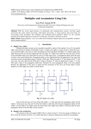
  • 1. IOSR Journal of Electronics and Communication Engineering (IOSR-JECE) e-ISSN: 2278-2834,p- ISSN: 2278-8735.Volume 10, Issue 1, Ver. 1 (Jan - Feb. 2015), PP 36-44 www.iosrjournals.org DOI: 10.9790/2834-10113644 www.iosrjournals.org 36 | Page Multiplier and Accumulator Using Csla Asst Prof, Anoop M M Electronics and Communication Engineering MG University College Of Engineering And Technology,Thodupuzha Abstract: With the recent rapid advances in multimedia and communication systems, real-time signal processing like audio signal processing, video/image processing, or large-capacity data processing are increasingly being demanded. The multiplier and multiplier-and-accumulator (MAC) are the essential elements of the digital signal processing such as filtering, convolution, and Inner products. Index Terms: Booth multiplier, carry save adder,Booth multiplier,Digital signal processing(DSP), multiplier and-accumulator(MAC). I. Introduction A. Ripple Carry Adder Multiple full adder circuits can be cascaded in parallel to add an N-bit number. For an N- bit parallel adder, there must be N number of full adder circuits. A ripple carry adder is a logic circuit in which the carry- out of each full adder is the carry in of the succeeding next most significant full adder. It is called a ripple carry adder because each carry bit gets rippled into the next stage. In a ripple carry adder the sum and carry out bits of any half adder stage is not valid until the carry in of that stage occurs. A propagation delay inside the logic circuitry is the reason behind this. Propagation delay is time elapsed between the application of an input and occurrence of the corresponding output. Consider a NOT gate, When the input is “0″ the output will be “1″ and vice versa. The time taken for the NOT gate‟s output to become “0″ after the application of logic “1″ to the NOT gate‟s input is the propagation delay here. Similarly the carry propagation delay is the time elapsed between the application of the carry in signal and the occurrence of the carry out (Cout) signal. Circuit diagram of a 4-bit ripple carry adder is shown below. Fig. 3.1. Ripple carry adder Sum out S0 and carry out Cout of the Full Adder 1 is valid only after the propagation delay of Full Adder 1. In the same way, Sum out S3 of the Full Adder is valid only after the joint propagation delays of Full Adder 1 to Full Adder 4. In simple words, the final result of the ripple carry adder is valid only after the joint propagation delays of all full adder circuits inside it. B. Regular Csla Architecture The structure of the 16-b regular SQRT CSLA is shown in Fig.3.2. It has five groups of different size RCA. From the structure of CSLA, it is evident that there is scope for reducing area and power consumption.
  • 2. Multiplier and Accumulator Using Csla DOI: 10.9790/2834-10113644 www.iosrjournals.org 37 | Page Fig.3.2.16B-Regular CSLA Architecture Fig.3.2(a).Group2 of 16B CSLA Fig.3.2(b).Group3 of 16B CSLA Fig.3.2(c).Group4 of 16B CSLA
  • 3. Multiplier and Accumulator Using Csla DOI: 10.9790/2834-10113644 www.iosrjournals.org 38 | Page Fig.3.2 (d).Group5 of 16B CSLA The steps leading to the evaluation are as follows. 1) The group2 [see Fig.3.2(a)] has two sets of 2-b RCA. Based on the consideration of delay values of Table I, the arrival time of selection input c1[time(t)=7] of 6:3 mux is earlier than s3[t=8] and later than s2[t=6]. Thus, sum3[t=11] is summation ofs3 and mux[t=3] and sum2[t=10] is summation of c1 and mux. 2) Except for group2, the arrival time of mux selection input is always greater than the arrival time of data outputs from the RCA‟s. Thus, the delay of group3 to group5 is determined, respectively as follows: (3.1) (3.2) (3.3) 3) The one set of 2-b RCA in group2 has 2 FA for Cin=1 and the other set has 1 FA and 1 HA for Cin=0. Based on the area count the total number of gate counts in group2 is determined as follows: … (3.4) … (3.5) … (3.6) … (3.7) GROUP DELAY AREA GROUP2 11 57 GROUP3 13 87 GROUP4 16 117 GROUP5 19 147 Table 3.1: Delay and Area of Regular CSLA Groups 4) Similarly, the estimated maximum delay and area of the other groups in the regular SQRT CSLA are evaluated and listed in Table 3.1. The carry out calculated from the last stage i.e. least significant bit stage is used to select the actual calculated values of the output carry and sum. The selection is done by using a multiplexer. Internal structure of the group 2 of regular 16-bit CSLA is shown Fig.3.2(a). By manually counting the number of gates used for group 2 is 57 (full adder, half adder, and multiplexer). One input to the mux goes from the RCA with Cin=0 and other input from the RCA with Cin=1. 3.3. Csla Using Bec 1.1. 1. Binary to excess convertor 1 Excess-1 binary coded decimal (XS-1) or Stibitz code, also called biased representation or Excess-N, is a complementary BCD code and numeral system. Excess-1 was used on some older computers as well as in cash registers and hand held portable electronic calculators of the 1970's, among other uses. It is a way to represent values with a balanced number of positive and negative numbers using a pre-specified number N as a biasing value. It is a non weighted code. In XS-1, numbers are represented as decimal digits, and each digit is represented by four bits as the digit value plus 1 (the "excess" amount) To reduce the area and power consumption of regular CSLA, RCA with Cin=1 is replaced with BEC. An n+1 bit BEC replaces the n bit RCA. The function table of a 3-b BEC is shown in Fig.3.3. and Table3.3
  • 4. Multiplier and Accumulator Using Csla DOI: 10.9790/2834-10113644 www.iosrjournals.org 39 | Page respectively. By the use of BEC logic, we can reduce the significant amount of silicon area reduction in the VLSI design. The Boolean expressions of the 3-bit BEC are given below. S0 = ~ B0 (3.8) S1 = B0 ^ B1 (3.9) S2 = B2 ^ (B0 & B1) (3.10) Fig.3.3. Binary to Excess Convertor-I Fig.3.4. Binary to Excess Convertor-I ADDER BLOCKS DELAY AREA XOR 3 5 2:1 MUX 3 4 HALF ADDER 3 6 FULL ADDER 6 13 Table 3.2. Delay and Area Count of the Basic Blocks of CSLA BINARY VALUE BEC-1 0000 0001 0001 0010 0010 0011 0011 0100 0100 0101 0101 0110 0110 0111 0111 1000 1000 1001 1001 1010 1010 1011 1011 1100 1100 1101 1101 1110 1110 1111 1111 0000 Table 3.3.Binary to BEC I Truth Table(4-Bit) 3.3.2. Architecture of CSLA with BEC The Binary to excess one Converter (BEC) replaces the ripple carry adder with Cin=1, in order to reduce the area and power consumption of the regular CSLA. The modified16-bit CSLA using BEC is shown in Fig.3.4. The structure is again divided into five groups with different bit size RCA and BEC. The group 2 of the modified 16-bit CSLA is shown Fig. 6. By manually counting the number of gates used for group 2 is 43 (full adder, half adder, multiplexer, BEC).
  • 5. Multiplier and Accumulator Using Csla DOI: 10.9790/2834-10113644 www.iosrjournals.org 40 | Page Fig. 3.4.16B-Modified CSLA architecture Fig.3.4 (a).Group 2 of Modified CSLA Architecture Fig. 3.4 (b).Group 3 of Modified CSLA Architecture Fig. 3.4 (c).Group 4 of Modified CSLA Architecture
  • 6. Multiplier and Accumulator Using Csla DOI: 10.9790/2834-10113644 www.iosrjournals.org 41 | Page Fig. 3.4 (d).Group 5 of Modified CSLA Architecture One input to the mux goes from the RCA with Cin=0 and other input from the BEC. Comparing the group 2 of both regular and modified CSLA, it is clear that BEC structure reduces the area and power. But the disadvantage of BEC method is that the delay is increasing than the regular CSLA. The steps leading to the evaluation are given here. 1) The group2 [see Fig.3.4(a)] has one 2-b RCA which has 1 FA and 1 HA for Cin=0. Instead of another 2-b RCA with Cin=1 a 3-b BEC is used which adds one to the output from 2-b RCA. Based on the consideration of delay values, the arrival time of selection input c1[time(t)=7] of 6:3 mux is earlier than the and s3[t=9] and c3[t=10] and later than the s2[t=4]. Thus, the sum3 and final c3 (output from mux) are depending on s3 and mux and partial c3 (input to mux) and mux, respectively. The sum2 depends on c1 and mux 2) For the remaining group‟s the arrival time of mux selection input is always greater than the arrival time of data inputs from the BEC‟s. Thus, the delay of the remaining groups depends on the arrival time of mux selection input and the mux delay. 3) The area count of group2 is determined as follows: (3.11) (3.12) (3.13) (3.14) (3.15) (3.16) (3.17) (3.18) GROUP DELAY AREA GROUP2 13 43 GROUP3 16 61 GROUP4 19 84 GROUP5 22 107 Table 3.4. Delay and Area count of Modified CSLA 4) Similarly, the estimated maximum delay and area of the other groups of the modified SQRT CSLA are evaluated and listed in Table.3.4. 1.2. Csla Using D-Latch 3.4.1. D-latch One very useful variation on the RS latch circuit is the Data latch, or D latch as it is generally called. As shown in the logic diagram below, the D latch is constructed by using the inverted S input as the R input signal. The single remaining input is designated "D" to distinguish its operation from other types of latches. It
  • 7. Multiplier and Accumulator Using Csla DOI: 10.9790/2834-10113644 www.iosrjournals.org 42 | Page makes no difference that the R input signal is effectively clocked twice, since the CLK signal will either allow the signals to pass both gates or it will not. Fig.3.5. D-Latch Structure In the D latch, when the CLK input is logic 1, the Q output will always reflect the logic level present at the D input, no matter how that changes. When the CLK input falls to logic 0, the last state of the D input is trapped and held in the latch, for use by whatever other circuits may need this signal. Because the single D input is also inverted to provide the signal to reset the latch, this latch circuit cannot experience a "race" condition caused by all inputs being at logic 1 simultaneously. Therefore the D latch circuit can be safely used in any circuit. Although the D latch does not have to be made edge triggered for safe operation, there are some applications where an edge-triggered D flip-flop is desirable. This can be accomplished by using a D latch circuit as the master section of an RS flip-flop. Both types are useful, so both are made commercially available. Except for the change in input circuitry, a D flip-flop works just like the RS flip-flop. 3.4.2. Architecture of CSLA with D latch In this method replace any one of the RCA structure ( i.e. cin =1 or cin =0) by parallel structure of D- latches. For n bit RCA structure it required n D-latches with enable pin as a clk. Latches are used to store one bit information. The RCA structure cin is replace by enable pin , where enable signal is clk signal. When enable pin en =1 then the RCA structure is calculate for cin=1 that result is stored in D-latch. When en =0 then it will calculate for cin =0 and the D-latch output and full adder output is given to the mux. By using selection line it will gives the proper output. Where the enable time period for „1‟ is very less when compared to the enable pin „0‟. Initially RCA structure will calculate for en=1 and then en =0. The architecture of proposed 16-b CSLA is shown in Fig. 10. It has different five groups of different bit size RCA and D-Latch. Instead of using two separate adders in the regular CSLA, in this method only one adder is used to reduce the area, power consumption and delay. Each of the two additions is performed in one clock cycle. This is 16-bit adder in which least significant bit (LSB) adder is ripple carry adder, which is 2 bit wide. The upper half of the adder i.e., most significant part is 14-bit wide which works according to the clock. Whenever clock goes high addition for carry input one is performed. When clock goes low then carry input is assumed as zero and sum is stored in adder itself. Latch is used to store the sum and carry for Cin=1. Carry out from the previous stage i.e., least significant bit adder is used as control signal for multiplexer to select final output carry and sum of the 16-bit adder. If the actual carry input is one, then computed sum and carry latch is accessed and for carry input zero MSB adder is accessed. Cout is the output carry. The Fig.9 shows the internal structure of group 2 to 5 of the proposed 16-bit CSLA. Fig.3.6 (a). Internal structure of 3 D-latches in parallel
  • 8. Multiplier and Accumulator Using Csla DOI: 10.9790/2834-10113644 www.iosrjournals.org 43 | Page Fig.3.6(b). Internal structure of 4 D-latches in parallel Fig. 3.6(c). Internal structure of 5 D-latches in parallel Fig.3.6 (d). Internal structure of 6 D-latches in parallel block of Fig.10
  • 9. Multiplier and Accumulator Using Csla DOI: 10.9790/2834-10113644 www.iosrjournals.org 44 | Page Fig.3.6. internal structures of Proposed CSLA by using D-Latch Fig.3.7. CSLA using D-Latch 1.3. Research methodologies and approach This project is aimed for implementing high performance optimized FPGA architecture. This work has been developed using Verilog-HDL. Isim 13.3 is used for simulating the CSLA and synthesized using Xilinx PlanAhead13.3. Xilinx is commonly available tool. Availability is the main reason to select this tool for doing the project. In this project I tried to reduce the delay a little bit by using Xilinx synthesis technique. These synthesis techniques promote fast and efficient FPGA design development. There are many synthesis options that can help you to obtain your performance and area objectives. Here I use the timing constraints to drive the optimization. References [1]. Fayez Elguibaly, “ A fast parallel multiplier –accumulator using the modified booth algorithm,” IEEE Trans on Circuits and systems,vol.47,September 2000 [2]. Young-Ho Seo,Dong –Wook Kim,” A New VLSI Architecture of Parallel Multiplier and Accumulator Based on Radix-2 Modified Booth Algorithm,”IEEE Trans.on VLSI,vol.18,February 2012 [3]. B Rajani kumari,K.V Ramana Rao,”Dynamic Power Suppression Technique in Booth Multipliers”,IJITEE 2278-3075, Volume-1, Issue-4, September 2012 [4]. G.Sasi,”Design of Low Power /High Speed Multiplier Using Spurious Power Suppression Technique” IJCSMC, Vol. 3, Issue. 1, January 2014, pg.37 – 41 [5]. R.Sheshadri M.E,” Spurious Power Suppression Technique for VLSI Architecure”,IJCSE Vol. 3 No.6 Dec 2012-Jan 2013