
Recommandé
Contenu connexe
Similaire à module 4.pptx
Similaire à module 4.pptx (20)
Dernier
Dernier (20)
module 4.pptx
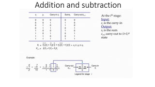
- 7. Fast addition –carry look ahead adder
- 8. CARRY LOOK AHEAD ADDER
- 9. MULTIPLICATION OF POSITIVE NUMBERS
- 17. ⦁ The ALU performs arithmetic operations on the 2 operands applied to its A and B inputs. ⦁ One of the operands is output of MUX; ⦁ The result (produced by the ALU) is stored temporarily in register Z. ⦁ The sequence of operations for [R3] [R1]+[R2] is as follows: 1. R1out, Yin 2. R2out, SelectY, Add, Zin 3. Zout, R3in ⦁ Instruction execution proceeds as follows: Step 1 --> Contents from register R1 are loaded into register Y. Step2 --> Contents from Y and from register R2 are applied to the A and B inputs of ALU; Addition is performed & Result is stored in the Z register. Step 3 --> The contents of Z register is stored in the R3 register. ⦁ The signals are activated for the duration of the clock cycle corresponding to that step. All other signals are inactive.
- 18. • CONTROL-SIGNALS OF MDR • ⦁ The MDR register has 4 control-signals • 1. MDRin & MDRout control the connection to the internal processor data bus & 2. MDRinE & MDRoutE control the connection to the memory Data bus. ⦁ MAR register has 2 control-signals. • 1. MARin controls the connection to the internal processor address bus & 2. MARout controls the connection to the memory address bus.
- 19. FETCHING A WORD FROM MEMORY 1) Mov (r1) , r2 R1out, MARin, Read ;desired address is loaded into MAR & Read command is issued. 2) MDRinE, WMFC ;load MDR from memory-bus & Wait for MFC response from memory. 3) MDRout, R2in ;load R2 from MDR. where WMFC=control-signal that causes processor's control. circuitry to wait for arrival of MFC signal. Storing a Word in Memory Consider the instruction MOVE R2,(R1). This requires the following sequence: 1) R1out, MARin ;desired address is loaded into MAR. 2) R2out, MDRin, Write ;data to be written are loaded into MDR & Write command is issued. 3) MDRoutE, WMFC ;load data into memory-location pointed by R1 from MDR.
- 20. EXECUTION OF A COMPLETE INSTRUCTION Consider the instruction ADD (R3),R1 which adds the contents of a memory-location pointed by R3 to register R1. Executing this instruction requires the following actions: ADD (R3),R1 Fetch the instruction. Fetch the first operand. Perform the addition & Load the result into R1.
- 21. Instruction execution proceeds as follows: Step1 loading contents of PC into MAR & sending a Read request to memory. The Select signal is set to Select4, which causes the Mux to select constant 4. This value is added to operand at input B (PC‟s content), and the result is stored in Z. Step2--> Updated value in Z is moved to PC. This completes the PC increment operation and PC will now point to next instruction. Step3--> Fetched instruction is moved into MDR and then to IR. The step 1 through 3 constitutes the Fetch Phase. At the beginning of step 4, the instruction decoder interprets the contents of the IR. This enables the control circuitry to activate the control-signals for steps 4 through 7. The step 4 through 7 constitutes the Execution Phase. Step4--> Contents of R3 are loaded into MAR & a memory read signal is issued. Step5--> Contents of R1 are transferred to Y to prepare for addition. Step6--> When Read operation is completed, memory-operand is available in MDR, and the addition is performed. Step7--> Sum is stored in Z, then transferred to R1.The End signal causes a new instruction fetch cycle to begin by returning to step1.
- 23. Hardwired control unit • To execute the instructions, the processor must have some means of generating the control signals needed in the proper sequence. Two categories : • Hardwired control and • microprogrammed control.