SlideShare une entreprise Scribd logo
1  sur  29
MSI Shift Registers
• 74LS194 4-Bit
  Bidirectional Universal
  Shift Register
• may be used in the
  following data register
  transfers
  –   serial-serial,
  –   shift left,
  –   shift right,
  –   serial-parallel,
  –   parallel-serial,
  –   and parallel-parallel


                                        1
MSI Shift Registers
• 74LS194 4-Bit Bidirectional Universal Shift
  Register


                                                2
MSI Shift Registers
• 74LS194 control inputs S1 and S0


                                     3
MSI Shift Registers
• 74LS194 4-Bit Bidirectional Universal Shift
  Register


         01   11   10   00   01   11   10   00   01   11   10   00   01   11   10   00


                                                                                         4
MSI Shift Registers
• 74LS194 4-Bit Bidirectional Universal Shift
  Register


                                                5
“Universal”
shift register
  74x194
• Shift left
• Shift right
• Load
• Hold


                 6
MSI Shift Registers
• One stage of the 74x194


                                 7
MSI Shift Register 74195


or D0–D3
MSI Shift Register 74195
• 74195 logic diagram
                /P0     /P1   /P2    /P3
Ring Counter
• A ring counter is a loop of flip-flops interconnected in such
  a manner that only one of the devices may be in a specified
  state at one time
• If the specified state is HIGH, then only one device may be
  HIGH at one time.
• As the clock, or input, signal is received, the specified state
  will shift to the next device at a rate of 1 shift per clock, or
  input, pulse.


                                                                14
MSI Shift Registers
• 74LS194 control inputs S1 and S0


                                     15
Shift-Register
  Counters
• Ring counter
• For Shift right
S0Vcc, S1 for Load and Reset,
  AVcc, BCD Gnd,
QD RIN, LIN is not connected


                                 16
Ring counter (Self correcting)
• 4 bit, 4 state with a single circulating 1
State diagram for a self correcting ring counter


                   0001              0000
            0010          1000

    1001           0100                 1100

         1010                 0110                    1110
  0101          1101   0011          1011      0111          1111
Ring counter (Self correcting)
• 4 bit, 4 state with a single circulating 0
Johnson Counter (“Twisted ring” counter)


                                    20
Timing diagram for a 4-bit Johnson counter


                                             21
States of an 4-bit Johnson counter
State       Q3     Q2       Q1        Q0       Decoding
Name

    S1         0        0        0         0    Q3’•Q0’
    S2         0        0        0         1    Q1’•Q0
    S3         0        0        1         1    Q2’•Q0
    S4         0        1        1         1    Q3’•Q2
    S5         1        1        1         1    Q3•Q0
    S6         1        1        1         0    Q1•Q0’
    S7         1        1        0         0    Q2•Q1’
    S8         1        0        0         0    Q3•Q2’

* Can be decoded with 2-input gates
Self correcting Johnson Counter
                  • n-bit counter
                  • 2n - 2n unused states
                  • 0x…x0 → 00…01
                  • 2 input NOR gate
                    performs correction


                                    23
Linear Feedback Shift Register Counter
• n-bit shift register counters have far less than the
  maximum number of 2n normal states
• n states for ring counter, 2n states for Johnson counter
• An n-bit LFSR counter can have 2n – 1 states
  also called as maximum length sequence generator
• Design is based on the theory of finite fields
• Developed by French mathematician Evariste Galois
• Serial input is connected to the sum modulo 2 of a
  certain set of output bits
• These feedback connections determine the state
  sequence of the counter
• By convention, outputs are always numbered and
  shifted in the direction shown in figure on next slide
• There exists at least one equation which makes the counter go
  through all the 2n - 1 states before repeating
• It can never cycle through all 2n states
• Regardless of the connection pattern 0…0 → 0…0
                                                          25
Feedback
equations
for LFSR
counters


            26
3-bit LFSR counter      Sequence
                          X2    X1    X0
                          1     0     0
                          0     1     0
                          1     0     1
                          1     1     0
                          1     1     1
                          0     1     1
                 X2
                 X1
                          0     0     1
                 X0       1     0     0


X3
Modified LFSR Counter
• An LFSR can be modified to have 2n states including the
  all 0’s state
• In an n-bit LFSR counter, an extra EXOR gate and an n
  – 1 input NOR gate connected to all the shift register
  outputs except X0 accomplishes the task
• The states are not visited in binary order
• Usually used where this characteristic is an advantage
  -     Generating test inputs for logic circuits
  -     Encoding and decoding circuits for certain error-
        detecting and error-correcting codes including
  CRC codes
  -     Scrambling and descrambling data patterns in data
        communications
  -     Pseudo random binary sequence generator
Modified 3-bit LFSR counter to include all 0’s
                                           Sequence
                                          X2     X1   X0
                                          1      0    0
                                          0      1    0
                                          1      0    1
                                          1      1    0
                                          1      1    1
                                          0      1    1
                                          0      0    1
                                          0      0    0
                            X2            1      0    0
                             X1
                             X0


        X3

Contenu connexe

Tendances

Sigma-Delta Analog to Digital Converters
Sigma-Delta Analog to Digital ConvertersSigma-Delta Analog to Digital Converters
Sigma-Delta Analog to Digital ConvertersSatish Patil
 
14827 shift registers
14827 shift registers14827 shift registers
14827 shift registersSandeep Kumar
 
Verilog VHDL code Decoder and Encoder
Verilog VHDL code Decoder and EncoderVerilog VHDL code Decoder and Encoder
Verilog VHDL code Decoder and EncoderBharti Airtel Ltd.
 
Flip-Flop || Digital Electronics
Flip-Flop || Digital ElectronicsFlip-Flop || Digital Electronics
Flip-Flop || Digital ElectronicsMd Sadequl Islam
 
INTERFACING ANALAOG TO DIGITAL CONVERTER (ADC0808/09) TO 8051 MICROCONTROLLER
 INTERFACING ANALAOG TO DIGITAL CONVERTER (ADC0808/09) TO 8051 MICROCONTROLLER   INTERFACING ANALAOG TO DIGITAL CONVERTER (ADC0808/09) TO 8051 MICROCONTROLLER
INTERFACING ANALAOG TO DIGITAL CONVERTER (ADC0808/09) TO 8051 MICROCONTROLLER SIRILsam
 
Divide by N clock
Divide by N clockDivide by N clock
Divide by N clockMantra VLSI
 
3 Bit Synchronous Down Counter
3 Bit Synchronous Down Counter3 Bit Synchronous Down Counter
3 Bit Synchronous Down CounterRabin BK
 
Sequential circuits in Digital Electronics
Sequential circuits in Digital ElectronicsSequential circuits in Digital Electronics
Sequential circuits in Digital ElectronicsVinoth Loganathan
 
Switched capacitor
Switched capacitorSwitched capacitor
Switched capacitorGur Kan
 
555 Timer integrated circuit and its applications
555 Timer integrated circuit and its applications555 Timer integrated circuit and its applications
555 Timer integrated circuit and its applicationsMayank Raj Singh
 

Tendances (20)

Sigma-Delta Analog to Digital Converters
Sigma-Delta Analog to Digital ConvertersSigma-Delta Analog to Digital Converters
Sigma-Delta Analog to Digital Converters
 
14827 shift registers
14827 shift registers14827 shift registers
14827 shift registers
 
D latch
D latchD latch
D latch
 
Verilog VHDL code Decoder and Encoder
Verilog VHDL code Decoder and EncoderVerilog VHDL code Decoder and Encoder
Verilog VHDL code Decoder and Encoder
 
Counter
CounterCounter
Counter
 
Pass Transistor Logic
Pass Transistor LogicPass Transistor Logic
Pass Transistor Logic
 
Sequential circuits
Sequential circuitsSequential circuits
Sequential circuits
 
Flip-Flop || Digital Electronics
Flip-Flop || Digital ElectronicsFlip-Flop || Digital Electronics
Flip-Flop || Digital Electronics
 
Timer 555
Timer 555Timer 555
Timer 555
 
INTERFACING ANALAOG TO DIGITAL CONVERTER (ADC0808/09) TO 8051 MICROCONTROLLER
 INTERFACING ANALAOG TO DIGITAL CONVERTER (ADC0808/09) TO 8051 MICROCONTROLLER   INTERFACING ANALAOG TO DIGITAL CONVERTER (ADC0808/09) TO 8051 MICROCONTROLLER
INTERFACING ANALAOG TO DIGITAL CONVERTER (ADC0808/09) TO 8051 MICROCONTROLLER
 
Divide by N clock
Divide by N clockDivide by N clock
Divide by N clock
 
CMOS Logic Circuits
CMOS Logic CircuitsCMOS Logic Circuits
CMOS Logic Circuits
 
Lecture 5
Lecture 5Lecture 5
Lecture 5
 
3 Bit Synchronous Down Counter
3 Bit Synchronous Down Counter3 Bit Synchronous Down Counter
3 Bit Synchronous Down Counter
 
Sequential circuits in Digital Electronics
Sequential circuits in Digital ElectronicsSequential circuits in Digital Electronics
Sequential circuits in Digital Electronics
 
Flipflop
FlipflopFlipflop
Flipflop
 
Switched capacitor
Switched capacitorSwitched capacitor
Switched capacitor
 
Counters
CountersCounters
Counters
 
555 Timer integrated circuit and its applications
555 Timer integrated circuit and its applications555 Timer integrated circuit and its applications
555 Timer integrated circuit and its applications
 
Logic families
Logic  familiesLogic  families
Logic families
 

En vedette

Sequential Circuits - Flip Flops
Sequential Circuits - Flip FlopsSequential Circuits - Flip Flops
Sequential Circuits - Flip FlopsAbhilash Nair
 
Introduction to VHDL - Part 1
Introduction to VHDL - Part 1Introduction to VHDL - Part 1
Introduction to VHDL - Part 1Abhilash Nair
 
VHDL - Enumerated Types (Part 3)
VHDL - Enumerated Types (Part 3)VHDL - Enumerated Types (Part 3)
VHDL - Enumerated Types (Part 3)Abhilash Nair
 
Synchronous design process
Synchronous design processSynchronous design process
Synchronous design processAbhilash Nair
 
Designing Clocked Synchronous State Machine
Designing Clocked Synchronous State MachineDesigning Clocked Synchronous State Machine
Designing Clocked Synchronous State MachineAbhilash Nair
 
State Machine Design and Synthesis
State Machine Design and SynthesisState Machine Design and Synthesis
State Machine Design and SynthesisAbhilash Nair
 
Static and Dynamic Read/Write memories
Static and Dynamic Read/Write memoriesStatic and Dynamic Read/Write memories
Static and Dynamic Read/Write memoriesAbhilash Nair
 
Analysis of state machines & Conversion of models
Analysis of state machines & Conversion of modelsAnalysis of state machines & Conversion of models
Analysis of state machines & Conversion of modelsAbhilash Nair
 
Iaetsd an mtcmos technique for optimizing low
Iaetsd an mtcmos technique for optimizing lowIaetsd an mtcmos technique for optimizing low
Iaetsd an mtcmos technique for optimizing lowIaetsd Iaetsd
 
Programmable PN Sequence Generators
Programmable PN Sequence GeneratorsProgrammable PN Sequence Generators
Programmable PN Sequence GeneratorsRajesh Singh
 
Vlsi ii project presentation
Vlsi ii project presentationVlsi ii project presentation
Vlsi ii project presentationRedwan Islam
 
03 shift registers_and_more_data_manipulation_sp15
03 shift registers_and_more_data_manipulation_sp1503 shift registers_and_more_data_manipulation_sp15
03 shift registers_and_more_data_manipulation_sp15John Todora
 
software development life cycle
software development life cyclesoftware development life cycle
software development life cycleAnanthachethan
 

En vedette (20)

CPLDs
CPLDsCPLDs
CPLDs
 
Sequential Circuits - Flip Flops
Sequential Circuits - Flip FlopsSequential Circuits - Flip Flops
Sequential Circuits - Flip Flops
 
Shift Registers
Shift RegistersShift Registers
Shift Registers
 
Introduction to VHDL - Part 1
Introduction to VHDL - Part 1Introduction to VHDL - Part 1
Introduction to VHDL - Part 1
 
VHDL Part 4
VHDL Part 4VHDL Part 4
VHDL Part 4
 
VHDL - Enumerated Types (Part 3)
VHDL - Enumerated Types (Part 3)VHDL - Enumerated Types (Part 3)
VHDL - Enumerated Types (Part 3)
 
VHDL - Part 2
VHDL - Part 2VHDL - Part 2
VHDL - Part 2
 
Synchronous design process
Synchronous design processSynchronous design process
Synchronous design process
 
Designing Clocked Synchronous State Machine
Designing Clocked Synchronous State MachineDesigning Clocked Synchronous State Machine
Designing Clocked Synchronous State Machine
 
State Machine Design and Synthesis
State Machine Design and SynthesisState Machine Design and Synthesis
State Machine Design and Synthesis
 
Static and Dynamic Read/Write memories
Static and Dynamic Read/Write memoriesStatic and Dynamic Read/Write memories
Static and Dynamic Read/Write memories
 
Shift registers
Shift registersShift registers
Shift registers
 
Chapter 6 register
Chapter 6 registerChapter 6 register
Chapter 6 register
 
Analysis of state machines & Conversion of models
Analysis of state machines & Conversion of modelsAnalysis of state machines & Conversion of models
Analysis of state machines & Conversion of models
 
Iaetsd an mtcmos technique for optimizing low
Iaetsd an mtcmos technique for optimizing lowIaetsd an mtcmos technique for optimizing low
Iaetsd an mtcmos technique for optimizing low
 
Programmable PN Sequence Generators
Programmable PN Sequence GeneratorsProgrammable PN Sequence Generators
Programmable PN Sequence Generators
 
Vlsi ii project presentation
Vlsi ii project presentationVlsi ii project presentation
Vlsi ii project presentation
 
03 shift registers_and_more_data_manipulation_sp15
03 shift registers_and_more_data_manipulation_sp1503 shift registers_and_more_data_manipulation_sp15
03 shift registers_and_more_data_manipulation_sp15
 
Fpga technology
Fpga technologyFpga technology
Fpga technology
 
software development life cycle
software development life cyclesoftware development life cycle
software development life cycle
 

Similaire à MSI Shift Registers

Counter with memes
Counter with memesCounter with memes
Counter with memesLee Diaz
 
Counter with memes
Counter with memesCounter with memes
Counter with memesLee Diaz
 
Digital Counter Design
 Digital Counter Design Digital Counter Design
Digital Counter DesignGargiKhanna1
 
Synchronous Sequential Logic Unit 4
Synchronous Sequential Logic Unit 4Synchronous Sequential Logic Unit 4
Synchronous Sequential Logic Unit 4Asif Iqbal
 
dsd-II-unit-III-registers-counters (1).pptx
dsd-II-unit-III-registers-counters (1).pptxdsd-II-unit-III-registers-counters (1).pptx
dsd-II-unit-III-registers-counters (1).pptxssuser1b2fab
 
Computer system architecture 16 counters
Computer system architecture 16 countersComputer system architecture 16 counters
Computer system architecture 16 countersthearticlenow
 
Sequential Circuits - Flip Flops (Part 2)
Sequential Circuits - Flip Flops (Part 2)Sequential Circuits - Flip Flops (Part 2)
Sequential Circuits - Flip Flops (Part 2)Abhilash Nair
 
digital elctronics
digital elctronicsdigital elctronics
digital elctronicsAsif Iqbal
 

Similaire à MSI Shift Registers (20)

Counter
CounterCounter
Counter
 
Counter with memes
Counter with memesCounter with memes
Counter with memes
 
Counter with memes
Counter with memesCounter with memes
Counter with memes
 
Digital Counter Design
 Digital Counter Design Digital Counter Design
Digital Counter Design
 
Counters
CountersCounters
Counters
 
Counters
CountersCounters
Counters
 
Synchronous Sequential Logic Unit 4
Synchronous Sequential Logic Unit 4Synchronous Sequential Logic Unit 4
Synchronous Sequential Logic Unit 4
 
dsd-II-unit-III-registers-counters (1).pptx
dsd-II-unit-III-registers-counters (1).pptxdsd-II-unit-III-registers-counters (1).pptx
dsd-II-unit-III-registers-counters (1).pptx
 
Ca lec12
Ca lec12Ca lec12
Ca lec12
 
Computer system architecture 16 counters
Computer system architecture 16 countersComputer system architecture 16 counters
Computer system architecture 16 counters
 
MSI Counters
MSI CountersMSI Counters
MSI Counters
 
Counters
CountersCounters
Counters
 
Sequential Circuits - Flip Flops (Part 2)
Sequential Circuits - Flip Flops (Part 2)Sequential Circuits - Flip Flops (Part 2)
Sequential Circuits - Flip Flops (Part 2)
 
digital elctronics
digital elctronicsdigital elctronics
digital elctronics
 
3.pdf
3.pdf3.pdf
3.pdf
 
Shift register
Shift registerShift register
Shift register
 
COUNTERS.pptx
COUNTERS.pptxCOUNTERS.pptx
COUNTERS.pptx
 
FF and Latches.ppt
FF and Latches.pptFF and Latches.ppt
FF and Latches.ppt
 
LFSR Lecture
LFSR LectureLFSR Lecture
LFSR Lecture
 
Project lfsr
Project lfsrProject lfsr
Project lfsr
 

Plus de Abhilash Nair

Plus de Abhilash Nair (15)

Feedback Sequential Circuits
Feedback Sequential CircuitsFeedback Sequential Circuits
Feedback Sequential Circuits
 
Designing State Machine
Designing State MachineDesigning State Machine
Designing State Machine
 
Analysis of state machines
Analysis of state machinesAnalysis of state machines
Analysis of state machines
 
Sequential Circuits - Flip Flops (Part 1)
Sequential Circuits - Flip Flops (Part 1)Sequential Circuits - Flip Flops (Part 1)
Sequential Circuits - Flip Flops (Part 1)
 
FPGA
FPGAFPGA
FPGA
 
FPLDs
FPLDsFPLDs
FPLDs
 
CPLDs
CPLDsCPLDs
CPLDs
 
CPLD & FPLD
CPLD & FPLDCPLD & FPLD
CPLD & FPLD
 
CPLDs
CPLDsCPLDs
CPLDs
 
Documentation Standards of an IC
Documentation Standards of an ICDocumentation Standards of an IC
Documentation Standards of an IC
 
EPROM, PROM & ROM
EPROM, PROM & ROMEPROM, PROM & ROM
EPROM, PROM & ROM
 
Trends Of Televisions
Trends Of TelevisionsTrends Of Televisions
Trends Of Televisions
 
Core java slides
Core java slidesCore java slides
Core java slides
 
Vectors in Java
Vectors in JavaVectors in Java
Vectors in Java
 
Arrays in Java
Arrays in JavaArrays in Java
Arrays in Java
 

Dernier

Class 11th Physics NEET formula sheet pdf
Class 11th Physics NEET formula sheet pdfClass 11th Physics NEET formula sheet pdf
Class 11th Physics NEET formula sheet pdfAyushMahapatra5
 
Russian Escort Service in Delhi 11k Hotel Foreigner Russian Call Girls in Delhi
Russian Escort Service in Delhi 11k Hotel Foreigner Russian Call Girls in DelhiRussian Escort Service in Delhi 11k Hotel Foreigner Russian Call Girls in Delhi
Russian Escort Service in Delhi 11k Hotel Foreigner Russian Call Girls in Delhikauryashika82
 
Call Girls in Dwarka Mor Delhi Contact Us 9654467111
Call Girls in Dwarka Mor Delhi Contact Us 9654467111Call Girls in Dwarka Mor Delhi Contact Us 9654467111
Call Girls in Dwarka Mor Delhi Contact Us 9654467111Sapana Sha
 
1029 - Danh muc Sach Giao Khoa 10 . pdf
1029 -  Danh muc Sach Giao Khoa 10 . pdf1029 -  Danh muc Sach Giao Khoa 10 . pdf
1029 - Danh muc Sach Giao Khoa 10 . pdfQucHHunhnh
 
Accessible design: Minimum effort, maximum impact
Accessible design: Minimum effort, maximum impactAccessible design: Minimum effort, maximum impact
Accessible design: Minimum effort, maximum impactdawncurless
 
Advanced Views - Calendar View in Odoo 17
Advanced Views - Calendar View in Odoo 17Advanced Views - Calendar View in Odoo 17
Advanced Views - Calendar View in Odoo 17Celine George
 
Measures of Central Tendency: Mean, Median and Mode
Measures of Central Tendency: Mean, Median and ModeMeasures of Central Tendency: Mean, Median and Mode
Measures of Central Tendency: Mean, Median and ModeThiyagu K
 
Paris 2024 Olympic Geographies - an activity
Paris 2024 Olympic Geographies - an activityParis 2024 Olympic Geographies - an activity
Paris 2024 Olympic Geographies - an activityGeoBlogs
 
Software Engineering Methodologies (overview)
Software Engineering Methodologies (overview)Software Engineering Methodologies (overview)
Software Engineering Methodologies (overview)eniolaolutunde
 
9548086042 for call girls in Indira Nagar with room service
9548086042  for call girls in Indira Nagar  with room service9548086042  for call girls in Indira Nagar  with room service
9548086042 for call girls in Indira Nagar with room servicediscovermytutordmt
 
social pharmacy d-pharm 1st year by Pragati K. Mahajan
social pharmacy d-pharm 1st year by Pragati K. Mahajansocial pharmacy d-pharm 1st year by Pragati K. Mahajan
social pharmacy d-pharm 1st year by Pragati K. Mahajanpragatimahajan3
 
Arihant handbook biology for class 11 .pdf
Arihant handbook biology for class 11 .pdfArihant handbook biology for class 11 .pdf
Arihant handbook biology for class 11 .pdfchloefrazer622
 
SOCIAL AND HISTORICAL CONTEXT - LFTVD.pptx
SOCIAL AND HISTORICAL CONTEXT - LFTVD.pptxSOCIAL AND HISTORICAL CONTEXT - LFTVD.pptx
SOCIAL AND HISTORICAL CONTEXT - LFTVD.pptxiammrhaywood
 
Unit-IV- Pharma. Marketing Channels.pptx
Unit-IV- Pharma. Marketing Channels.pptxUnit-IV- Pharma. Marketing Channels.pptx
Unit-IV- Pharma. Marketing Channels.pptxVishalSingh1417
 
Holdier Curriculum Vitae (April 2024).pdf
Holdier Curriculum Vitae (April 2024).pdfHoldier Curriculum Vitae (April 2024).pdf
Holdier Curriculum Vitae (April 2024).pdfagholdier
 
Q4-W6-Restating Informational Text Grade 3
Q4-W6-Restating Informational Text Grade 3Q4-W6-Restating Informational Text Grade 3
Q4-W6-Restating Informational Text Grade 3JemimahLaneBuaron
 
microwave assisted reaction. General introduction
microwave assisted reaction. General introductionmicrowave assisted reaction. General introduction
microwave assisted reaction. General introductionMaksud Ahmed
 
A Critique of the Proposed National Education Policy Reform
A Critique of the Proposed National Education Policy ReformA Critique of the Proposed National Education Policy Reform
A Critique of the Proposed National Education Policy ReformChameera Dedduwage
 

Dernier (20)

Class 11th Physics NEET formula sheet pdf
Class 11th Physics NEET formula sheet pdfClass 11th Physics NEET formula sheet pdf
Class 11th Physics NEET formula sheet pdf
 
Russian Escort Service in Delhi 11k Hotel Foreigner Russian Call Girls in Delhi
Russian Escort Service in Delhi 11k Hotel Foreigner Russian Call Girls in DelhiRussian Escort Service in Delhi 11k Hotel Foreigner Russian Call Girls in Delhi
Russian Escort Service in Delhi 11k Hotel Foreigner Russian Call Girls in Delhi
 
Call Girls in Dwarka Mor Delhi Contact Us 9654467111
Call Girls in Dwarka Mor Delhi Contact Us 9654467111Call Girls in Dwarka Mor Delhi Contact Us 9654467111
Call Girls in Dwarka Mor Delhi Contact Us 9654467111
 
1029 - Danh muc Sach Giao Khoa 10 . pdf
1029 -  Danh muc Sach Giao Khoa 10 . pdf1029 -  Danh muc Sach Giao Khoa 10 . pdf
1029 - Danh muc Sach Giao Khoa 10 . pdf
 
Accessible design: Minimum effort, maximum impact
Accessible design: Minimum effort, maximum impactAccessible design: Minimum effort, maximum impact
Accessible design: Minimum effort, maximum impact
 
Advanced Views - Calendar View in Odoo 17
Advanced Views - Calendar View in Odoo 17Advanced Views - Calendar View in Odoo 17
Advanced Views - Calendar View in Odoo 17
 
Measures of Central Tendency: Mean, Median and Mode
Measures of Central Tendency: Mean, Median and ModeMeasures of Central Tendency: Mean, Median and Mode
Measures of Central Tendency: Mean, Median and Mode
 
Paris 2024 Olympic Geographies - an activity
Paris 2024 Olympic Geographies - an activityParis 2024 Olympic Geographies - an activity
Paris 2024 Olympic Geographies - an activity
 
Software Engineering Methodologies (overview)
Software Engineering Methodologies (overview)Software Engineering Methodologies (overview)
Software Engineering Methodologies (overview)
 
9548086042 for call girls in Indira Nagar with room service
9548086042  for call girls in Indira Nagar  with room service9548086042  for call girls in Indira Nagar  with room service
9548086042 for call girls in Indira Nagar with room service
 
social pharmacy d-pharm 1st year by Pragati K. Mahajan
social pharmacy d-pharm 1st year by Pragati K. Mahajansocial pharmacy d-pharm 1st year by Pragati K. Mahajan
social pharmacy d-pharm 1st year by Pragati K. Mahajan
 
Arihant handbook biology for class 11 .pdf
Arihant handbook biology for class 11 .pdfArihant handbook biology for class 11 .pdf
Arihant handbook biology for class 11 .pdf
 
SOCIAL AND HISTORICAL CONTEXT - LFTVD.pptx
SOCIAL AND HISTORICAL CONTEXT - LFTVD.pptxSOCIAL AND HISTORICAL CONTEXT - LFTVD.pptx
SOCIAL AND HISTORICAL CONTEXT - LFTVD.pptx
 
Unit-IV- Pharma. Marketing Channels.pptx
Unit-IV- Pharma. Marketing Channels.pptxUnit-IV- Pharma. Marketing Channels.pptx
Unit-IV- Pharma. Marketing Channels.pptx
 
Holdier Curriculum Vitae (April 2024).pdf
Holdier Curriculum Vitae (April 2024).pdfHoldier Curriculum Vitae (April 2024).pdf
Holdier Curriculum Vitae (April 2024).pdf
 
Q4-W6-Restating Informational Text Grade 3
Q4-W6-Restating Informational Text Grade 3Q4-W6-Restating Informational Text Grade 3
Q4-W6-Restating Informational Text Grade 3
 
microwave assisted reaction. General introduction
microwave assisted reaction. General introductionmicrowave assisted reaction. General introduction
microwave assisted reaction. General introduction
 
INDIA QUIZ 2024 RLAC DELHI UNIVERSITY.pptx
INDIA QUIZ 2024 RLAC DELHI UNIVERSITY.pptxINDIA QUIZ 2024 RLAC DELHI UNIVERSITY.pptx
INDIA QUIZ 2024 RLAC DELHI UNIVERSITY.pptx
 
A Critique of the Proposed National Education Policy Reform
A Critique of the Proposed National Education Policy ReformA Critique of the Proposed National Education Policy Reform
A Critique of the Proposed National Education Policy Reform
 
Mattingly "AI & Prompt Design: Structured Data, Assistants, & RAG"
Mattingly "AI & Prompt Design: Structured Data, Assistants, & RAG"Mattingly "AI & Prompt Design: Structured Data, Assistants, & RAG"
Mattingly "AI & Prompt Design: Structured Data, Assistants, & RAG"
 

MSI Shift Registers

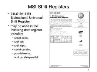
  • 1. MSI Shift Registers • 74LS194 4-Bit Bidirectional Universal Shift Register • may be used in the following data register transfers – serial-serial, – shift left, – shift right, – serial-parallel, – parallel-serial, – and parallel-parallel 1
  • 2. MSI Shift Registers • 74LS194 4-Bit Bidirectional Universal Shift Register 2
  • 3. MSI Shift Registers • 74LS194 control inputs S1 and S0 3
  • 4. MSI Shift Registers • 74LS194 4-Bit Bidirectional Universal Shift Register 01 11 10 00 01 11 10 00 01 11 10 00 01 11 10 00 4
  • 5. MSI Shift Registers • 74LS194 4-Bit Bidirectional Universal Shift Register 5
  • 6. “Universal” shift register 74x194 • Shift left • Shift right • Load • Hold 6
  • 7. MSI Shift Registers • One stage of the 74x194 7
  • 8.
  • 11. MSI Shift Register 74195 or D0–D3
  • 13. MSI Shift Register 74195 • 74195 logic diagram /P0 /P1 /P2 /P3
  • 14. Ring Counter • A ring counter is a loop of flip-flops interconnected in such a manner that only one of the devices may be in a specified state at one time • If the specified state is HIGH, then only one device may be HIGH at one time. • As the clock, or input, signal is received, the specified state will shift to the next device at a rate of 1 shift per clock, or input, pulse. 14
  • 15. MSI Shift Registers • 74LS194 control inputs S1 and S0 15
  • 16. Shift-Register Counters • Ring counter • For Shift right S0Vcc, S1 for Load and Reset, AVcc, BCD Gnd, QD RIN, LIN is not connected 16
  • 17. Ring counter (Self correcting) • 4 bit, 4 state with a single circulating 1
  • 18. State diagram for a self correcting ring counter 0001 0000 0010 1000 1001 0100 1100 1010 0110 1110 0101 1101 0011 1011 0111 1111
  • 19. Ring counter (Self correcting) • 4 bit, 4 state with a single circulating 0
  • 20. Johnson Counter (“Twisted ring” counter) 20
  • 21. Timing diagram for a 4-bit Johnson counter 21
  • 22. States of an 4-bit Johnson counter State Q3 Q2 Q1 Q0 Decoding Name S1 0 0 0 0 Q3’•Q0’ S2 0 0 0 1 Q1’•Q0 S3 0 0 1 1 Q2’•Q0 S4 0 1 1 1 Q3’•Q2 S5 1 1 1 1 Q3•Q0 S6 1 1 1 0 Q1•Q0’ S7 1 1 0 0 Q2•Q1’ S8 1 0 0 0 Q3•Q2’ * Can be decoded with 2-input gates
  • 23. Self correcting Johnson Counter • n-bit counter • 2n - 2n unused states • 0x…x0 → 00…01 • 2 input NOR gate performs correction 23
  • 24. Linear Feedback Shift Register Counter • n-bit shift register counters have far less than the maximum number of 2n normal states • n states for ring counter, 2n states for Johnson counter • An n-bit LFSR counter can have 2n – 1 states also called as maximum length sequence generator • Design is based on the theory of finite fields • Developed by French mathematician Evariste Galois • Serial input is connected to the sum modulo 2 of a certain set of output bits • These feedback connections determine the state sequence of the counter • By convention, outputs are always numbered and shifted in the direction shown in figure on next slide
  • 25. • There exists at least one equation which makes the counter go through all the 2n - 1 states before repeating • It can never cycle through all 2n states • Regardless of the connection pattern 0…0 → 0…0 25
  • 27. 3-bit LFSR counter Sequence X2 X1 X0 1 0 0 0 1 0 1 0 1 1 1 0 1 1 1 0 1 1 X2 X1 0 0 1 X0 1 0 0 X3
  • 28. Modified LFSR Counter • An LFSR can be modified to have 2n states including the all 0’s state • In an n-bit LFSR counter, an extra EXOR gate and an n – 1 input NOR gate connected to all the shift register outputs except X0 accomplishes the task • The states are not visited in binary order • Usually used where this characteristic is an advantage - Generating test inputs for logic circuits - Encoding and decoding circuits for certain error- detecting and error-correcting codes including CRC codes - Scrambling and descrambling data patterns in data communications - Pseudo random binary sequence generator
  • 29. Modified 3-bit LFSR counter to include all 0’s Sequence X2 X1 X0 1 0 0 0 1 0 1 0 1 1 1 0 1 1 1 0 1 1 0 0 1 0 0 0 X2 1 0 0 X1 X0 X3