Micro-Scholarship, What it is, How can it help me.pdf
Registers and counters
1. MODULE 4 MCA-102 DIGITAL SYSTEMS & LOGIC DESIGN ADMN 2014-‘17
Dept. of Computer Science And Applications, SJCET, Palai Page 77
4.1 Introduction
Registers are groups of flip-flops, where each flip-flop is capable of storing one bit of information.
An n-bit register is a group of n flip-flops. The basic function of a register is to hold information in a digital
system and make it available to the logic elements for the computing process. Registers consist of a finite
number of flip-flops. Since each flip-flop is capable of storing either a "0" or a "1", there is a finite number
of 0-1 combinations that can be stored into a register. Each of those combinations is known
as state or content of the register. With flip-flops we can store data bitwise but usually data does not appear
as single bits. Instead it is common to store data words of n bit with typical word lengths of 4, 8, 16, 32 or
64 bit. Thus, several flip-flops are combined to form a register to store whole data words. Registers are
synchronous circuits thus all flip-flops are controlled by a common clock line. As registers are often used
to collect serial data they are also called accumulators.
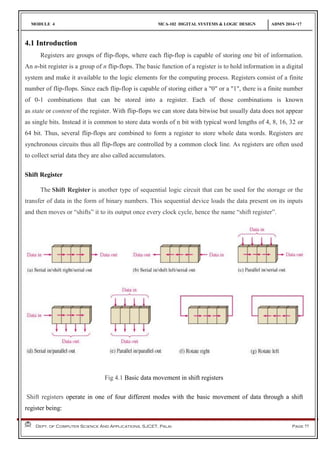
Shift Register
The Shift Register is another type of sequential logic circuit that can be used for the storage or the
transfer of data in the form of binary numbers. This sequential device loads the data present on its inputs
and then moves or “shifts” it to its output once every clock cycle, hence the name “shift register”.
Fig 4.1 Basic data movement in shift registers
Shift registers operate in one of four different modes with the basic movement of data through a shift
register being:
2. MODULE 4 MCA-102 DIGITAL SYSTEMS & LOGIC DESIGN ADMN 2014-‘17
Dept. of Computer Science And Applications, SJCET, Palai Page 78
• Serial-in to Serial-out (SISO)
• Serial-in to Parallel-out (SIPO)
• Parallel-in to Serial-out (PISO)
• Parallel-in to parallel-out (PIPO)
4.2 Serial-in to Serial-out (SISO)
The data is shifted serially “IN” and “OUT” of the register, one bit at a time in either a left or
right direction under clock control.
It has only three connections, the serial input, which determines what enters the left hand flip-
flop, the serial output, which is taken from the output of the right hand flip-flop and the
sequencing clock signal. The logic circuit diagram below shows a generalized serial-in serial-out
shift register.
Fig 4.2 Serial-in to Serial-out (SISO) register
Fig 4.3 SISO input operations (1011)
3. MODULE 4 MCA-102 DIGITAL SYSTEMS & LOGIC DESIGN ADMN 2014-‘17
Dept. of Computer Science And Applications, SJCET, Palai Page 79
The above figure illustrates entry of the four bits 1010 into the register. After imputing of data’s, Four bits
(1010) being serially shifted out of the register and replaced by all zeros.
4.3 Serial-in to Parallel-out (SIPO)
The register is loaded with serial data, one bit at a time, with the stored data being available at
the output in parallel form.
Clock cycles are required to load a four bit word.
Fig 4.4 Serial-in to Parallel-out (SIPO) register
4.4 Parallel-in to Serial-out (PISO)
The parallel data is loaded into the register simultaneously and is shifted out of the register
serially one bit at a time under clock control.
The circuit shown below is a four bit parallel input serial output register.
Output of previous Flip Flop is connected to the input of the next one via a combinational circuit.
The binary input word B0, B1, B2, B3 is applied though the same combinational circuit.
There are two modes in which this circuit can work namely shift mode or load mode.
LOAD MODE
When the shift/load bar line is low (0), the AND gate 2, 4 and 6 become active. They will pass B1, B2, and
B3bits to the corresponding flip-flops. On the low going edge of clock, the binary input B0, B1, B2, B3 will
get loaded into the corresponding flip-flops. Thus parallel loading takes place.
SHIFT MODE
When the shift/load bar line is low (1), the AND gate 2, 4 and 6 become inactive. Hence the parallel
loading of the data becomes impossible. But the AND gate 1, 3 and 5 become active. Therefore the
4. MODULE 4 MCA-102 DIGITAL SYSTEMS & LOGIC DESIGN ADMN 2014-‘17
Dept. of Computer Science And Applications, SJCET, Palai Page 80
shifting of data from left to right bit by bit on application of clock pulses. Thus the parallel in serial out
operation take place.
Fig 4.5 PISO register
4.5 Parallel-in to parallel-out (PIPO)
The parallel data is loaded simultaneously into the register, and transferred together to their
respective outputs by the same clock pulse.
In this mode, the 4 bit binary input B0, B1, B2, B3 is applied to the data inputs D0, D1, D2, and
D3 respectively of the four flip-flops. As soon as a negative clock edge is applied, the input
binary bits will be loaded into the flip-flops simultaneously. The loaded bits will appear
simultaneously to the output side. Only clock pulse is essential to load all the bits.
Fig 4.6 PIPO register
5. MODULE 4 MCA-102 DIGITAL SYSTEMS & LOGIC DESIGN ADMN 2014-‘17
Dept. of Computer Science And Applications, SJCET, Palai Page 81
4.6 Bidirectional Shift Registers
A bidirectional, or reversible, shift register is one in which the data can be shift either left or right. A four-
bit bidirectional shift register using D flip-flops is shown below.
Fig 4.7 Bidirectional shift register
Here a set of NAND gates are configured as OR gates to select data inputs from the right or left adjacent
bistables, as selected by the LEFT/RIGHT control line.
With Right/Left = 1: Shift right operation
Then the AND gates 1, 3, 5 and 7 are enable whereas the remaining AND gates 2, 4, 6 and 8 will be
disabled.
The data is shifted to right bit by bit on the application of clock pulses. Thus we get the serial right
shift operation.
With Right/Left = 0: Shift left operation
When the mode control M is connected to 0 then the AND gates 2, 4, 6 and 8 are enabled while 1,
3, 5 and 7 are disabled.
The data is shifted left bit by bit on the application of clock pulses. Thus we get the serial right shift
operation.
6. MODULE 4 MCA-102 DIGITAL SYSTEMS & LOGIC DESIGN ADMN 2014-‘17
Dept. of Computer Science And Applications, SJCET, Palai Page 82
4.7 Universal Shift Register
A shift register which can shift the data in only one direction is called a uni-directional shift register. A
shift register which can shift the data in both directions is called a bi-directional shift register. Applying the
same logic, a shift register which can shift the data in both directions as well as load it parallel, then it is
known as a universal shift register. The shift register is capable of performing the following operation
Parallel loading
Lift shifting
Right shifting
The mode control input is connected to logic 1 for parallel loading operation whereas it is connected to 0
for serial shifting. With mode control pin connected to ground, the universal shift register acts as a bi-
directional register. For serial left operation, the input is applied to the serial input which goes to AND
gate-1 shown in figure. Whereas for the shift right operation, the serial input is applied to D input.
Fig 4.8 Universal shift register
7. MODULE 4 MCA-102 DIGITAL SYSTEMS & LOGIC DESIGN ADMN 2014-‘17
Dept. of Computer Science And Applications, SJCET, Palai Page 83
4.8 COUNTER
Counter is a sequential circuit. A digital circuit which is used for a counting pulses is known counter.
Counter is the widest application of flip-flops. It is a group of flip-flops with a clock signal applied.
Counters are of two types.
Asynchronous or ripple counters: the first flip-flop is clocked by the external clock pulse, and then
each successive flip-flop is clocked by the Q or Q' output of the previous flip-flop.
Synchronous counters: all memory elements are simultaneously triggered by the same clock.
Synchronous counters are faster than asynchronous counter because in synchronous counter all flip flops
are clocked simultaneously.
• The number of flip-flops determines the count limit or number of states:
States = 2 ( no of flip-flops)
• The number of states used is called the MODULUS.
• For example, a Modulus-12 counter (Mod-12) would count from 0 (0000) to 11 (1011) and would
require four flip-flops (24
= 16 states; 12 are used)
Modulus Counter (MOD-N Counter)
The 2-bit ripple counter is called as MOD-4 counter and 3-bit ripple counter is called as MOD-8
counter. So in general, an n-bit ripple counter is called as modulo-N counter. Where, MOD number = 2n
Type of modulus
2-bit up or down (MOD-4)
3-bit up or down (MOD-8)
4-bit up or down (MOD-16)
Asynchronous or ripple counters
A two-bit asynchronous counter is shown below. The external clock is connected to the clock input of the
first flip-flop (FF0) only. So, FF0 changes state at the falling edge of each clock pulse, but FF1 changes
only when triggered by the falling edge of the Q output of FF0. Because of the inherent propagation delay
through a flip-flop, the transition of the input clock pulse and a transition of the Q output of FF0 can never
occur at exactly the same time. Therefore, the flip-flops cannot be triggered simultaneously, producing an
asynchronous operation.
8. MODULE 4 MCA-102 DIGITAL SYSTEMS & LOGIC DESIGN ADMN 2014-‘17
Dept. of Computer Science And Applications, SJCET, Palai Page 84
Fig 4.9 Two bit asynchronous ripple counter
The 2-bit ripple counter circuit above has four different states, each one corresponding to a count value.
Similarly, a counter with n flip-flops can have 2 to the power n states. The number of states in a counter is
known as its mod (modulo) number. Thus a 2-bit counter is a mod-4 counter.
Asynchronous Decade Counters
The binary counters previously introduced have two to the power n states. But counters with states less
than this number are also possible. They are designed to have the number of states in their sequences,
which are called truncated sequences. These sequences are achieved by forcing the counter to recycle
before going through all of its normal states. A common modulus for counters with truncated sequences is
ten. A counter with ten states in its sequence is called a decade counter. The circuit below is an
implementation of a decade counter.
Fig 4.10 Asynchronous Decade Counters
9. MODULE 4 MCA-102 DIGITAL SYSTEMS & LOGIC DESIGN ADMN 2014-‘17
Dept. of Computer Science And Applications, SJCET, Palai Page 85
Once the counter counts to ten (1010), all the flip-flops are being cleared. Notice that only Q1 and Q3 are
used to decode the count of ten. This is called partial decoding, as none of the other states (zero to nine)
have both Q1 and Q3 HIGH at the same time. The sequence of the decade counter is shown in the table
below:
Fig 4.11 binary sequence of decade counter
Asynchronous Up-Down Counters
The circuit below is a 3-bit up-down counter. It counts up or down depending on the status of the
control signals UP and DOWN. When the UP input is at 1 and the DOWN input is at 0, the NAND
network between FF0 and FF1 will gate the non-inverted output (Q) of FF0 into the clock input of FF1.
Similarly, Q of FF1 will be gated through the other NAND network into the clock input of FF2. Thus the
counter will count up.
Fig 4.12 Asynchronous Up-Down Counters
10. MODULE 4 MCA-102 DIGITAL SYSTEMS & LOGIC DESIGN ADMN 2014-‘17
Dept. of Computer Science And Applications, SJCET, Palai Page 86
When the control input UP is at 0 and DOWN is at 1, the inverted outputs of FF0 and FF1 are gated
into the clock inputs of FF1 and FF2 respectively. If the flip-flops are initially reset to 0's, then the counter
will go through the following sequence as input pulses are applied.
Fig 4.13 truth table of Asynchronous Up-Down Counters
Synchronous Counters
In synchronous counters, the clock inputs of all the flip-flops are connected together and are triggered by
the input pulses. Thus, all the flip-flops change state simultaneously (in parallel). The circuit below is a 3-
bit synchronous counter. The J and K inputs of FF0 are connected to HIGH. FF1 has its J and K inputs
connected to the output of FF0, and the J and K inputs of FF2 are connected to the output of an AND gate
that is fed by the outputs of FF0 and FF1.
Fig 4.14 3 bit synchronous counter with table
The most important advantage of synchronous counters is that there is no cumulative time delay
because all flip-flops are triggered in parallel.
11. MODULE 4 MCA-102 DIGITAL SYSTEMS & LOGIC DESIGN ADMN 2014-‘17
Dept. of Computer Science And Applications, SJCET, Palai Page 87
Synchronous Decade Counters
Similar to an asynchronous decade counter, a synchronous decade counter counts from 0 to 9 and then
recycles to 0 again. This is done by forcing the 1010 state back to the 0000 state. This so called truncated
sequence can be constructed by the following circuit.
Fig 4.15 Synchronous Decade Counters
From the sequence on the left, we notice that:
Q0 toggles on each clock pulse.
Q1 changes on the next clock pulse each time Q0=1 and
Q3=0.
Q2 changes on the next clock pulse each time Q0=Q1=1.
Q3 changes on the next clock pulse each time Q0=1, Q1=1
and Q2=1 (count 7), or when Q0=1 and Q3=1 (count 9).
Fig 4.16 Table of Synchronous Decade Counters
Synchronous Up-Down Counters
A circuit of a 3-bit synchronous up-down counter and a table of its sequence are shown below. Similar to
an asynchronous up-down counter, a synchronous up-down counter also has an up-down control input. It
is used to control the direction of the counter through a certain sequence.
12. MODULE 4 MCA-102 DIGITAL SYSTEMS & LOGIC DESIGN ADMN 2014-‘17
Dept. of Computer Science And Applications, SJCET, Palai Page 88
Fig 4.17 3 bit Synchronous Up-Down Counters
UP/DOWN Ripple Counters
In the UP/DOWN ripple counter all the FFs operate in the toggle mode. So either T flip-flops or JK flip-
flops are to be used. The LSB flip-flop receives clock directly. But the clock to every other FF is obtained
from (Q = Q bar) output of the previous FF.
UP counting mode (M=0) - The Q output of the preceding FF is connected to the clock of the next stage if
up counting is to be achieved. For this mode, the mode select input M is at
logic 0 (M=0).
DOWN counting mode (M=1) - If M =1, then the Q bar output of the preceding FF is connected to the
next FF. This will operate the counter in the counting mode.
Up/Down Synchronous Counter
An up/down counter is capable of progressing in either direction depending on a control input.
Fig 4.18 Up/Down Synchronous Counter
13. MODULE 4 MCA-102 DIGITAL SYSTEMS & LOGIC DESIGN ADMN 2014-‘17
Dept. of Computer Science And Applications, SJCET, Palai Page 89
Cascaded counters
Cascading is a method of achieving higher-modulus counters. For synchronous IC counters, the next
counter is enabled only when the terminal count of the previous stage is reached. Larger counters can be
built by combining smaller counters together .The rollover signal is used to communicate when the upper
counters should roll over .
Fig 4.19 Cascaded counters
Two types of counters – Asynchronous – Synchronous
Shift Register Counters
Two of the most common types of shift register counters are introduced here: the Ring counter and
the Johnson counter. They are basically shift registers with the serial outputs connected back to the serial
inputs in order to produce particular sequences. These registers are classified as counters because they
exhibit a specified sequence of states.
Ring Counters
A ring counter is basically a circulating shift register in which the output of the most significant stage
is fed back to the input of the least significant stage. The following is a 4-bit ring counter constructed from
D flip-flops. The output of each stage is shifted into the next stage on the positive edge of a clock pulse. If
the CLEAR signal is high, all the flip-flops except the first one FF0 are reset to 0. FF0 is preset to 1
instead.
14. MODULE 4 MCA-102 DIGITAL SYSTEMS & LOGIC DESIGN ADMN 2014-‘17
Dept. of Computer Science And Applications, SJCET, Palai Page 90
Fig 4.20 4 bit ring counter
Since the count sequence has 4 distinct states, the counter can be considered as a mod-4 counter.
Only 4 of the maximum 16 states are used, making ring counters very inefficient in terms of state usage.
But the major advantage of a ring counter over a binary counter is that it is self-decoding. No extra
decoding circuit is needed to determine what state the counter is in.
Johnson Counters
Fig 4.21 Johnson Counters
Johnson counters are a variation of standard ring counters, with the inverted output of the last stage
fed back to the input of the first stage. They are also known as twisted ring counters. An n-stage Johnson
counter yields a count sequence of length 2n, so it may be considered to be amod-2n counter. The circuit
above shows a 4-bit Johnson counter. The state sequence for the counter is given in the table as well as the
animation on the left.
15. MODULE 4 MCA-102 DIGITAL SYSTEMS & LOGIC DESIGN ADMN 2014-‘17
Dept. of Computer Science And Applications, SJCET, Palai Page 91
Application of the counters
Frequency counters
Digital clock
Time measurement
A to D converter
Frequency divider circuits
Digital triangular wave generator