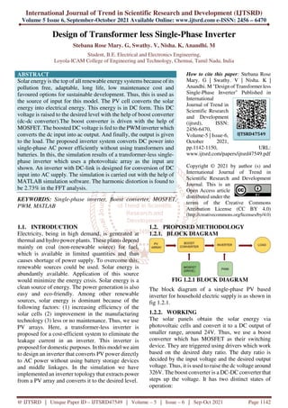
Solar energy is the top of all renewable energy systems because of its pollution free, adaptable, long life, low maintenance cost and favoured options for sustainable development. Thus, this is used as the source of input for this model. The PV cell converts the solar energy into electrical energy. This energy is in DC form. This DC voltage is raised to the desired level with the help of boost converter dc dc converter .The boost converter is driven with the help of MOSFET. The boosted DC voltage is fed to the PWM inverter which converts the dc input into ac output. And finally, the output is given to the load. The proposed inverter system converts DC power into single phase AC power efficiently without using transformers and batteries. In this, the simulation results of a transformer less single phase inverter which uses a photovoltaic array as the input are shown. An inverter with DC link is designed for conversion of DC input into AC supply. The simulation is carried out with the help of MATLAB simulation software. The harmonic distortion is found to be 2.73 in the FFT analysis. Stebana Rose Mary. G | Swathy. V | Nisha. K | Anandhi. M "Design of Transformer less Single-Phase Inverter" Published in International Journal of Trend in Scientific Research and Development (ijtsrd), ISSN: 2456-6470, Volume-5 | Issue-6 , October 2021, URL: https://www.ijtsrd.com/papers/ijtsrd47549.pdf Paper URL : https://www.ijtsrd.com/engineering/electrical-engineering/47549/design-of-transformer-less-singlephase-inverter/stebana-rose-mary-g
2. International Journal of Trend in Scientific Research and Development @ www.ijtsrd.com eISSN: 2456-6470
@ IJTSRD | Unique Paper ID – IJTSRD47549 | Volume – 5 | Issue – 6 | Sep-Oct 2021 Page 1143
(a)At ON-state: The current flows through the
inductor in clockwise-direction. The inductor stores
energy by generating a magnetic field. The polarity is
positive (left-side of the inductor).
(b)At OFF-state: The current is reduced as impedance
increases. The magnetic field created previously is
reduced in energy in order to maintain the current
towards the load. Thus, the polarity is reversed
(negative in the left side of the inductor).
A DC link is connected between the boost converter
and the inverter. It compensates the switching losses
caused by MOSFET switches and reduces the ripples.
And gives a filtered output from the boost converter
to the inverter. For this model we use a full bridge
inverter that converts the DC voltage to AC voltage.
This generates a square wave AC output voltage. We
also use a pulse width modulator (PWM) which
generates gate signals. A PWM signal is generated by
feeding a reference and a carrier signal through a
comparator which gives the output signal based on
the difference between the two inputs. The reference
is sinusoidal and the carrier wave is a triangle wave.
When the carrier wave exceeds reference, the output
is at one state and when the reference exceeds the
carrier, it is at the opposite state. Finally, the output
from the inverter (desired AC output) is fed to drive
loads.
1.3. SOFTWARE DEVELOPED
1.3.1. SOLAR PV ARRAY
A photovoltaic (PV) cell directly converts sunlight to
electricity through a process known as photovoltaic
effect. The PV cells absorb the photons emitted bythe
sun and generate a flow of electrons. These electrons
move to the n-side, while the holes are drifted
towards the p-side. Thus, a direct current is
established between the contacts. Since a typical
photovoltaic cell produces less than 3 watts at
approximately 0.5volt dc, cells must be connected in
series-parallel configurations to produce enough
power for high-power applications. Cells are
configured into modules and modules are connected
as arrays. Here we are using Beijing Zhongkexin
Electronics Equipment ZKX – 285 – 24 type array
module as an input to the inverter.
Maximum Power 285.326W
Open circuit Voltage Voc 44.8V
Voltageat maximum power point Vmp 35.8V
Short circuit current Isc 8.45A
Current at maximum power point Imp 7.97A
Cells per module 72
Series connected module sperstring 1
Parallel strings 5
MODULE DATA
PV ARRAY PLOT
The Irradiance and temperature values are adjusted
such that we obtain a DC voltage of approximately
24V for which the system is designed. Here the
values of Irradiance and temperature used are shown
in table below.
Irradiance 1000W/m²
Temperature 25deg.C.
ARRAY INPUT DATA
1.3.2. BOOST CONVERTER
A DC-DC converter is an electronic circuit which
converts a source of direct current (DC) from one
voltage level to another. The DC-DC converters are
widely used in regulated switch-mode dc power
supplies and in dc motor drives applications. Often
the input of these converters is an unregulated dc
voltage, which is obtained by rectifying the line
voltage, and therefore it will fluctuate due to changes
in the line voltage magnitude. The boost converter is
used to step up the input voltage to a desired value
which is greater than the input supply. It consists of
an inductor (L) in series with the supply voltage (Vs).
A semiconductor switch is connected across the
inductance and supply. A filter capacitor (C) is used
across the load to remove the ripples from the output
voltage (Vo). The diode blocks the reverse flow of
output current when the switch is turned on.The
semiconductor is turned ON at the calculated duty
cycle and hence, the current flows through the
inductor from the supply and thus, stores energy. The
capacitor maintains the output voltage and supplies
the current (Io) when the switch is ON. Hence the
diode is reverse biased and does not conduct. When
the switch is turned OFF, the inductance generates a
large voltage / to maintain the current in the
same direction. Here, the diode is forward biased and
it starts conducting. Thus, the output voltage will be
as eqt(1).
= + / ----------------------(1)
3. International Journal of Trend in Scientific Research and Development @ www.ijtsrd.com eISSN: 2456-6470
@ IJTSRD | Unique Paper ID – IJTSRD47549 | Volume – 5 | Issue – 6 | Sep-Oct 2021 Page 1144
Hence a greater output voltage is obtained than the supply voltage.
BOOST CONVERTER
Here, the boost converter is designed to provide a stepped-up output voltage of 326 V which is fed with an input
supply of 24 V from the PV array. The proposed converter is designed for a power rating of 500 W.
DC OUTPUT VOLTAGE OF BOOST CONVERTER
PARAMETERS VALUES
Inductor(L) 30µH
Capacitor(C) 0.1mF
Resistor(R) 212.5Ω
CONVERTER PARAMETERS
1.3.3. DC LINK
The DC link capacitor (C) is common to the boost converter and the single-phase inverter. It is used to filter the
ripples from the output of the boost converter and provides a steady DC voltage to the inverter circuit.
/(2 * * △ ) -------------------------(2)
1.3.4. SINGLE PHASE INVERTER
An inverter is used to change the input DC supply to a symmetric AC voltage of desired magnitude and
frequency. A variable output voltage is obtained by varying the input DC voltage and maintaining the gain of the
inverter constant. If the DC voltage is fixed and it’s not controllable, a variable output voltage can be obtained
by varying the gain of the inverter. Here, the gain of the inverter is varied by using a pulse width modulator
(PWM). The inverter gain is defined as the ratio of output voltage to the DC input voltage. An inverter is called a
voltage fed inverter (VFI) if the input voltage remains constant, a current fed inverter (CFI) if the input current is
4. International Journal of Trend in Scientific Research and Development @ www.ijtsrd.com eISSN: 2456-6470
@ IJTSRD | Unique Paper ID – IJTSRD47549 | Volume – 5 | Issue – 6 | Sep-Oct 2021 Page 1145
maintained constant and a variable DC linked inverter if the input voltage is controllable. These inverters are
used in various industrial applications like variable speed AC motor drives, induction heating, standby power
supplies and uninterruptible power supply. The typical single and three phase outputs are, 120 V at 60 Hz, 220 V
at 50 Hz, 115 V at 400 Hz, 220 to 380 V at 50 Hz, 120 to 208 V at 60 Hz and 115 to 200 V at 400 Hz.
SINGLE-PHASE INVERTER
The proposed model here, has a single-phase inverter with MOSFET as the semiconductor switch such that it
converts the 326 V DC supply from the boost converter to an AC voltage of range 150 to 220 V. The MOSFETs
are triggered using a pulse width modulator circuit. The inverted voltage is then passed through a filter circuit to
reduce the ripples and provide a steady AC supply to the load.
OUTPUTVOLTAGEANDCURRENTOFSINGLE-PHASEINVERTER
5. International Journal of Trend in Scientific Research and Development @ www.ijtsrd.com eISSN: 2456-6470
@ IJTSRD | Unique Paper ID – IJTSRD47549 | Volume – 5 | Issue – 6 | Sep-Oct 2021 Page 1146
PARAMETERS VALUES
Inductor(L) 0.712mF
Capacitor(C) 1.42µH
FILTER PARAMETERS
1.3.5. SINUSOIDAL PULSECWIDTH MODULATOR
The sinusoidal pulse width modulator is used for the generation of the gating signals, to trigger the
semiconductor switches in the circuit. The signals are generated by comparing a sinusoidal reference signal with
the triangular carrier wave of frequency Fc. The frequency of the reference signal Fr determines the inverter
output frequency Fo and its peak amplitude controls the modulation index M, and Then in turn the rms output
voltage.
SINUSOIDAL PULSE WIDTH MODULATOR
The reference frequency Fr is taken as 50 Hz and the carrier frequency Fc is taken as 50 KHz. Both the waves
are compared and the output obtained is given as a pulse to the MOSFETs 1 and 3 and the complement of the
output is fed as a pulse to the other set of MOSFETs 2 and 4, as shown in single phase inverter diagram.
6. International Journal of Trend in Scientific Research and Development @ www.ijtsrd.com eISSN: 2456-6470
@ IJTSRD | Unique Paper ID – IJTSRD47549 | Volume – 5 | Issue – 6 | Sep-Oct 2021 Page 1147
PULSE WAVEFORM
1.4. DESIGN CALCULATION
A. BOOST CONVERTER
Vin = 24 V; Vo = 326 V; P =500W; Io = 2 A; R = 212.5 Ω; = 80%; fs = 25 KHz
Duty cycle = (1 − ( / )) * η -------------------------(3)
= (1 – (24/326)) * 0.8
= 0.9411
Inductor L = ( ( − )/(∆ * * ) ---------(4)
= (24(326 – 24)) / (29.64* 25k * 326)
= 30 µH
Capacitor C = ( * )/( * ∆ ) ----------------------(5)
= (1.692 * 0.9411) / (25k * 0.6369)
= 0.1 Mf
B. DC Link
Capacitor Cdc = /(2 * * △ ) ----------------------(6)
= 1.692/ (2*π * 25k * 5)
= 2.15 µH
Where, is the line frequency in rad/s and △ is the ripple in the DC bus voltage.
C. FILTER DESIGN FOR INVERTER
Vin = 350 V; Vo = 230 V; fo = 50 Hz; fc = 50 kHz; Iripple = 20%
Inductor L = /(4 * * △ ) ---------------------(7)
= 350/(4*50k*8.69*1.414*0.2)
= 0.712 mF
fc = 1/(2 * π * √ ) fc = fc/10
Capacitor = (10/(2 * π * )) ² * 1/L ----------------------(8)
= (10/2* * 50k) ² *(1/0.712 m)
= 1.42 µH
1.5. RESULTS AND DISCUSSION
EXPERIMENTAL OBSERVATION
LOAD VALUE Vo(V) Io(A)
R 50Ω 160 2.8
LOAD STATORCURRENT(A) SPEED(r.p.m)
Single phase induction motor 24 553.9
7. International Journal of Trend in Scientific Research and Development @ www.ijtsrd.com eISSN: 2456-6470
@ IJTSRD | Unique Paper ID – IJTSRD47549 | Volume – 5 | Issue – 6 | Sep-Oct 2021 Page 1148
VOLTAGE AND CURRENT WAVEFORM OF RESISTIVE LOAD
8. International Journal of Trend in Scientific Research and Development @ www.ijtsrd.com eISSN: 2456-6470
@ IJTSRD | Unique Paper ID – IJTSRD47549 | Volume – 5 | Issue – 6 | Sep-Oct 2021 Page 1149
MOTORLOADWAVEFORM
1.5.1. FFT ANALYSIS
FFT ANALYSIS OF OUTPUT VOLTAGE
The FFT analysis of the obtained output voltage is shown ,which has a total harmonic distortion of 2.73 %.
9. International Journal of Trend in Scientific Research and Development @ www.ijtsrd.com eISSN: 2456-6470
@ IJTSRD | Unique Paper ID – IJTSRD47549 | Volume – 5 | Issue – 6 | Sep-Oct 2021 Page 1150
1.6. CONCLUSION
PV is one of the most efficient sourcebecause it
produces electric energy from a free inexhaustible
source, the sun, using no moving parts, consuming no
fossil fuels, and creating no pollution or greenhouse
gases during the power generation Using simulation
results of the proposed design, it is shown that a PV
power can be efficiently converted into AC power
without using batteries and transformers. Also middle
linkages are omitted to make the system light,
compact and easy for installation. The designed
single-phase inverter works well with different types
of loads, hence it is also compatible to be used for
domestic loads like various household appliances.
REFERENCE
[1] P Hridya, P Saritha, "High gain single stage
inverter", Intelligent Computing
Instrumentation and Control Technologies
(ICICICT) 2017 International Conference on,
pp. 387-392, 2017.
[2] Ashvini, G., S. Kamalsakthi, and J. Baskaran.
"PWM based active low power boost DC-AC
inverter." Computation of Power, Energy
Information and Commuincation (ICCPEIC),
2017 International Conference on. IEEE, 2017.
[3] Single-Phase Bridge Inverter with Active
Power Decoupling Based on Buck-Boost
Converter (2018 IEEE Energy Conversion
Congress and Exposition (ECCE)).
[4] Dineshkumar, T., M. Mathankumar, and M.
Sundaram. "High efficient single stage single
phase boost inverter with minimized harmonic
distortion." Sustainable Green Buildings and
Communities (SGBC), International
Conference on. IEEE, 2016.
[5] Sudha Bhutada, S R Nigam, “Design &
Simulation Of Boost Converter For Solar
Application”, CiiT International Journal of
Programmable Device Circuits and Systems,
Vol 7, No 01, January 2015.
[6] Evaluation of DC-link Decoupling Using
Electrolytic or Polypropylene Film Capacitors
in Three-Phase Grid-Connected Photovoltaic
Inverters Baburaj Karanayil(1), Vassilios G.
Agelidis(1) and Josep Pou(1)(2) (1)Australian
Energy Research Institute, The University of
New South Wales, UNSW Sydney, NSW 2052,
Australia.
[7] Modeling and Design of Single-Phase PV
Inverter with MPPT Algorithm Applied to the
Boost Converter Electrical Department,
Laboratory of Renewable Energies and
Intelligent Systems (LERSI), Faculty of
Sciences and Technology, Sidi Mohamed Ben
Abdellah University of Fez, Morocco. 2INSA,
Euro-Méditerranée, EUROMED University,
Fez, Morocco.
[8] Application Report SLVA372C–November
2009–Revised January 2014 Basic Calculation
of a Boost Converter's Power Stage Texas
Instruments.
[9] Solar Energy Fed Single Phase Inverter
Through Boost Converter - Priya
Panneerselvam, Lavanya Subramaniam, Vimala
Perumal. International Journal of 33 Science,
Engineering and Technology Research
(IJSETR), Volume 3, Issue 12, December 2014.
[10] Single phase PWM inverter with close Loop
DC-DC Boost Converter For Solar Application
- Vimal M. Vaniya, Jaydeep G. Gajipara Prof.
Jayanti A. Jadav Department of electrical
engineering, Marwadi education foundation of
P. G. studies.