
Recommandé
Contenu connexe
Tendances
Tendances (20)
Similaire à Line regulation
Similaire à Line regulation (20)
Dernier
Dernier (20)
Line regulation
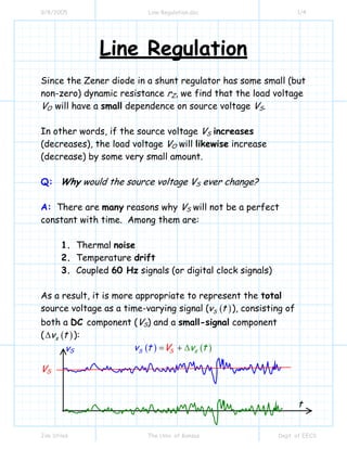
- 1. 9/8/2005 Line Regulation.doc 1/4 Jim Stiles The Univ. of Kansas Dept. of EECS Line Regulation Since the Zener diode in a shunt regulator has some small (but non-zero) dynamic resistance rZ, we find that the load voltage VO will have a small dependence on source voltage VS. In other words, if the source voltage VS increases (decreases), the load voltage VO will likewise increase (decrease) by some very small amount. Q: Why would the source voltage VS ever change? A: There are many reasons why VS will not be a perfect constant with time. Among them are: 1. Thermal noise 2. Temperature drift 3. Coupled 60 Hz signals (or digital clock signals) As a result, it is more appropriate to represent the total source voltage as a time-varying signal ( ( )Sv t ), consisting of both a DC component (VS) and a small-signal component ( ( )sv t∆ ): ( ) ( )S sS t vVv t= + ∆ VS vS t
- 2. 9/8/2005 Line Regulation.doc 2/4 Jim Stiles The Univ. of Kansas Dept. of EECS As a result of the small-signal source voltage, the total load voltage is likewise time-varying, with both a DC (VO) and small- signal ( ov∆ ) component: ( ) ( )O O ov t V v t= + ∆ So, we know that the DC source VS produces the DC load voltage VO, whereas the small-signal source voltage sv∆ results in the small-signal load voltage ov∆ . Q: Just how are sv∆ and ov∆ related? I mean, if sv∆ equals, say, 500 mV, what will value of ov∆ be? A: Determining this answer is easy! We simply need to perform a small-signal analysis. In other words, we first replace the Zener diode with its Zener PWL model. + - VS R RLO oV v+ ∆ + - + - sv∆
- 3. 9/8/2005 Line Regulation.doc 3/4 Jim Stiles The Univ. of Kansas Dept. of EECS We then turn off all the DC sources (including VZO) and analyze the remaining small-signal circuit! From voltage division, we find: Z L o s Z L r R v v R r R ⎛ ⎞ ∆ = ∆ ⎜ ⎟ +⎝ ⎠ However, recall that the value of a Zener dynamic resistance rZ is very small. Thus, we can assume that rZ >> RL, and therefore Z L Zr R r≈ , leading to: + - VS R RLO oV v+ ∆ + -rz + _ VZ0 + - sv∆ R RLov∆ + - + - sv∆ rz
- 4. 9/8/2005 Line Regulation.doc 4/4 Jim Stiles The Univ. of Kansas Dept. of EECS Z L o s Z L Z s Z r R v v R r R r v r R ⎛ ⎞ ∆ = ∆ ⎜ ⎟ +⎝ ⎠ ⎛ ⎞ ≈ ∆ ⎜ ⎟ +⎝ ⎠ Rearranging, we find: o Z s Z v r line regulation v r R ∆ = ∆ + This equation describes an important performance parameter for shunt regulators. We call this parameter the line regulation. * Line regulation allows us to determine the amount that the load voltage changes ( ov∆ ) when the source voltage changes ( sv∆ ). * For example, if line regulation is 0.002, we find that the load voltage will increase 1 mV when the source voltage increases 500mV (i.e., 0.002 0 002(0.5) 0.001 Vo sv v .∆ = ∆ = = ). * Ideally, line regulation is zero. Since dynamic resistance rZ is typically very small (i.e., Zr R ), we find that the line regulation of most shunt regulators is likewise small (this is a good thing!).