Le document traite des circuits FPGA et du langage VHDL, explorant leur histoire, leurs composants et leur programmation. Il aborde également les concepts fondamentaux de la conception électronique, des méthodologies, ainsi que des exemples d'expérimentations pratiques utilisant des FPGA. En outre, le document se concentre sur les étapes de programmation en VHDL, y compris les déclarations, les entités, et les processus de conception.


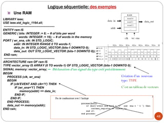
![Compteur
H
En
Q
R
Compteur
H
En
Q
R
Décodeur
7 Segments
In Out
Décodeur
7 Segments
In Out
CLK
U2
U1 U3
U4
Fil1[3..0]
Fil2[3..0]
Seg1[6..0]
Seg2[6..0]
19
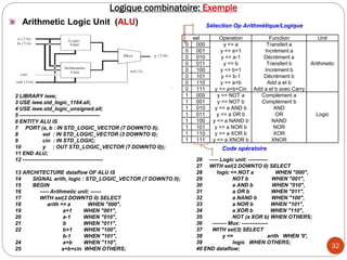
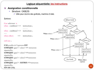
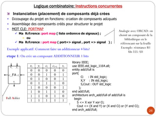
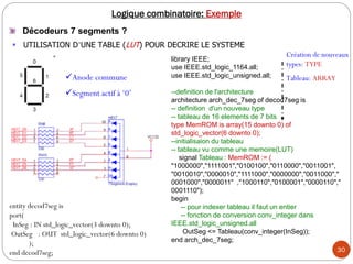
VHDL: Concepts de base
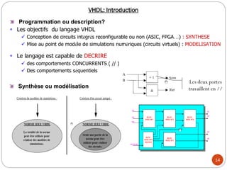
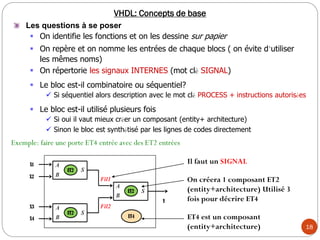
Un autre exemple: Horloge BCD 2 digits
Blocs décodeurs 7 segments - combinatoire
Blocs compteurs – séquentiel
Les Blocs compteurs sont cascadé pour la propagation de la retenue
Après 9 on a 0 avec 1 de retenue! Donc Affichage 10
Ce fil est interne au composant :
on le déclarera
SIGNAL FILS: bit_vector(3 downto 0);
Sorties pilotant les Leds
de l’afficheur 2
Séquentiel donc process
COMPT: PROCESS(CLK)
Begin
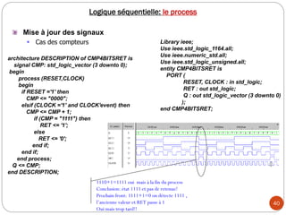
….
END PROCESS;](https://image.slidesharecdn.com/isertcoursvhdledasopcplatform-240308100729-64f59b85/85/COURS-VHDL-PROGRAMMATION-ET-_ETAPES-pour-comprendre-19-320.jpg)
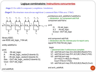
![22
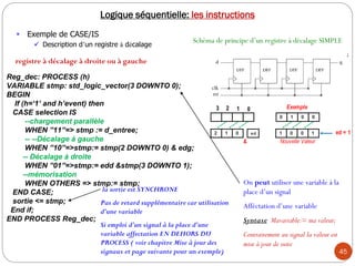
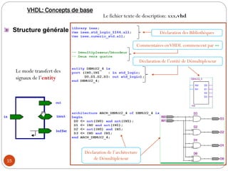
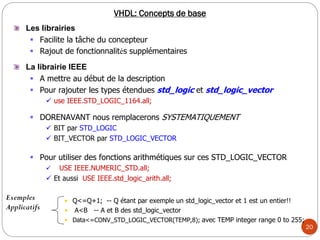
Les opérateurs
Logiques (boolean, bit, std_ulogic):
AND, OR, NAND, NOR, XOR,XNOR, NOT
Relationnels ( retournent un boolean):
=, /=, <, <=, >, >=
Arithmétiques:
+, -, *, /, **, MOD, REM, ABS
Concaténations d’éléments de tableaux &:
"bon" & "jour" => "bonjour"
Ne pas confondre 1 bit
‘0’ ou ‘1’
Avec un vecteur de bits
” 11 ” ou ” 1101110 ”
Un bus (ou ensemble de
fils électrique) est
représenté sous forme
d’un vecteur de bits
STD_LOGIC_VECTOR (3 DOWNTO 0);
VHDL: Concepts de base
Littéraux
Caractères: ’0’, ’x’,’a’,’%’
Chaînes: ”11110101”,”xx”,”bonjour”,”$@&”
Chaînes de bits: B”0010_1101”, X”2D”, O”055”
(Notation pour les vecteurs de bits dans différentes bases)
Décimaux:27, -5, 4e3, 76_562, 4.25
Basés: 2#1001#, 8#65_07, 16#C5#e2
(Notation pour les valeurs entières dans différentes bases)
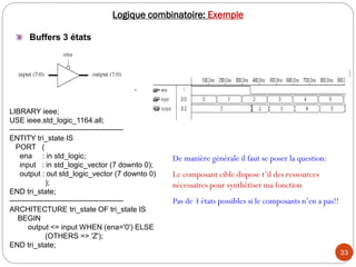
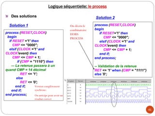
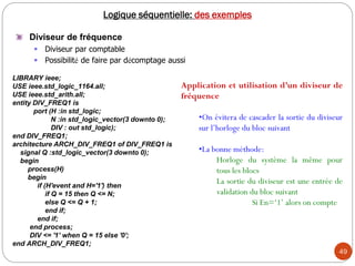
Encodeur
X[3..0]
Y[1..0]](https://image.slidesharecdn.com/isertcoursvhdledasopcplatform-240308100729-64f59b85/85/COURS-VHDL-PROGRAMMATION-ET-_ETAPES-pour-comprendre-22-320.jpg)
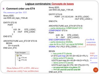
![23
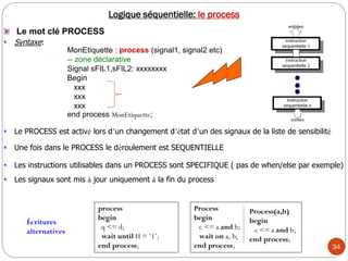
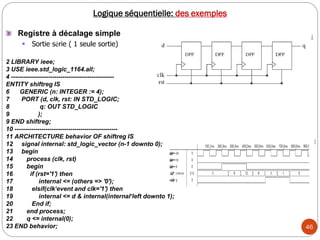
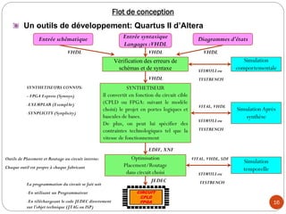
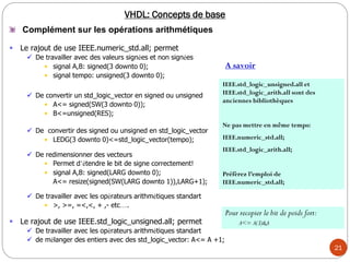
Assignation simples
library IEEE;
use IEEE.std_logic_1164.all;
--librairie pour inclure type std_logic
--portes ET
--3 entrées E2 E1 E0
-- 1 sortie S0
entity ET3 is
port (
E : IN std_logic_vector (2 downto 0);
S : OUT std_logic
);
end ET3;
--definition de l'architecture
architecture arch_ET3 of ET3 is
Begin
S<=E(2) and E(1) and E(0);
-- E(2) accès au fil 2
end arch_ET3;
library IEEE;
use IEEE.std_logic_1164.all;
entity exemple is
port (
E : IN std_logic_vector(2 downto 0);
S1 : OUT std_logic; --1 fil
S2,S3 : OUT std_logic_vector(3 downto 1); --3 fils S1[3:1]
S4 : OUT std_logic_vector(2 downto 0)
);
end exemple;
--définition de l'architecture
architecture arch_exemple of exemple is
begin
S1 <= '0';
S2 <= '1‘ & E(1 downto 0);
-- operateur COLLER (ou CONCATENE) &
-- S2(3) S2(2) S2(1)
-- '1' E(1) E(0)
S3 <= "101";
S4 <= "111" XOR E; --manip sur les bus directement
end arch_exemple;
Exemple 1 Exemple 2
Bit Poids fort
Bit Poids faible
Logique combinatoire: Instructions concurrentes](https://image.slidesharecdn.com/isertcoursvhdledasopcplatform-240308100729-64f59b85/85/COURS-VHDL-PROGRAMMATION-ET-_ETAPES-pour-comprendre-23-320.jpg)
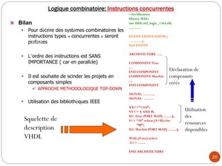
![24
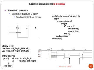
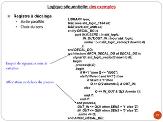
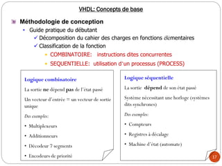
Logique combinatoire: Instructions concurrentes
Assignation conditionnelle
Structure WHEN/ELSE
---- Solution 1: WHEN/ELSE------
LIBRARY ieee;
use ieee.std_logic_1164.all;
entity encoder is
port ( x: in std_logic_vector (3 downto 0);
y: out std_logic_vector (1 downto 0));
end encoder;
architecture encoder1 of encoder is
begin
y <= "00" when x="0001" else
"01" when x="0010" else
"10" when x="0100" else
"11" when x="1000" else
"ZZ";
end encoder1;
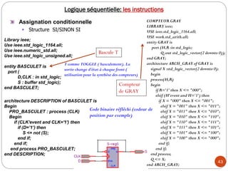
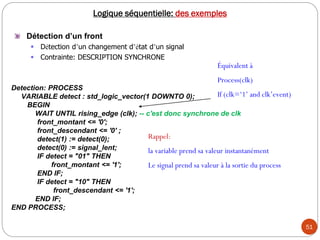
Exemple d’application:
encodeur clavier pour PIC
Intérêt: réduire le nombre d’entrée du PIC
signal <= signal_1 when expresion_boolénne else
………
signal_n when expresion_boolénne else
signal par défaut;
X[0]
X[1]
X[2]
X[3]
VCC
Encodeur
X[3..0]
Y[1..0]
n x m
Encodeur
(m-1:0)
......
X(1)
X(0)
X(n-2)
X(n-1)](https://image.slidesharecdn.com/isertcoursvhdledasopcplatform-240308100729-64f59b85/85/COURS-VHDL-PROGRAMMATION-ET-_ETAPES-pour-comprendre-24-320.jpg)
![31
Logique combinatoire: Exemple
Additionneur « haut niveau »
Emploi des librairies IEEE;
On augmente la taille de 1 si l’on
souhaite conserver la retenue d’entrée architecture arch1_add4full of adddirect is
--création de TEMP pour résultat: extension de 1 bit
signal TEMP : std_logic_vector(LARG downto 0);
begin
TEMP <= ('0'&A)+('0'&B)+Cin;
--A et B étendu chacun de 1 bit.
Res <= TEMP(TEMP'HIGH-1 downto 0);
Cout <= TEMP(TEMP'HIGH);
--TEMP'HIGH renvoi indice poids fort
end arch1_add4full;
library IEEE;
use IEEE.std_logic_1164.all;
use IEEE.std_logic_unsigned.all;
entity adddirect is
generic (LARG:integer:=4);
-- paramètre générique
-- taille additionneur changer en 1 clic!
port (
Cin : IN std_logic;
A : IN std_logic_vector(LARG-1 downto 0);
B : IN std_logic_vector(A'range);
Res : OUT std_logic_vector(A'range);
Cout : OUT std_logic
);
end adddirect;
Les attributs des signaux -Exemple S[5:0]
S’HIGH renvoie 5 et S’LOW renvoie 0
S’RANGE renvoie 5 downto 0
S’event renvoie TRUE si changement d’état de S
Utilisation de GENERIC lors du PORT MAP
U1: generic(10)
adddirect PORT MAP(xxxxxx);](https://image.slidesharecdn.com/isertcoursvhdledasopcplatform-240308100729-64f59b85/85/COURS-VHDL-PROGRAMMATION-ET-_ETAPES-pour-comprendre-31-320.jpg)