SlideShare une entreprise Scribd logo
1  sur  10
Télécharger pour lire hors ligne
ECE 414 F'’01 1 MHM
Simplified DAC / ADC Lecture Notes
This is a tutorial project to illustrate simplified operation of a Digital to Analog Converter
(DAC), and an Analog to Digital Converter (ADC).
Weighted Resistor Digital to Analog Converter
A schematic diagram of a weighted
summing amplifier is drawn to the
right. A switch connects an input
either to a common voltage V or to
a common ground. Only switches
currently connected to the voltage
source contribute current to the non-
inverting input summing node.
The output voltage is given by the
expression drawn below the circuit
diagram; SX = 1 if switch X
connects to V, SX = 0 if it connects
to ground. There are eight possible
combinations of connections for the
three switches, and these are indicated in the columns of the table to the right of the diagram. Each
combination is associated with a decimal integer as shown. The inputs are weighted in a 4:2:1
relationship, so that the sequence of values for 4S3 + 2S2 + S1 form a binary-coded decimal number
representation. The magnitude of Vo varies in units (steps) of (Rf/4R)V from 0 to 7. This circuit
provides a simplified Digital to Analog Converter (DAC). The digital input controls the switches, and
the amplifier provides the analog output.
Simplified PSpice Simulation
An illustrative circuit design is shown to the right,
with the switch arrangements replaced by three
square-wave voltage sources used to produce the
eight possible binary input voltage combinations.
A simplified circuit implemented in PSpice is shown
to the left. Pulse square-wave voltage sources are
used to provide the respective resistor inputs.
Various voltages are plotted below to illustrate
circuit behavior. The ‘binary’ input voltages are
drawn with an offset voltage is added to clarify the
drawings. The DAC output is shown in the
following plot. Note: the source voltages are defined
negative arbitrarily, simply to obtain a positive DAC
output after inversion.
ECE 414 F'’01 2 MHM
Alternative DAC Implementation
An alternative DAC illustration (Schematics) is drawn below. V0, V1, and V4 are square-wave pulse
sources with periods of 0.5ms, 1.0ms, and 2.0 ms respectively. The voltage-controlled switch pairs are
operated so that when one switch
is opened the other is closed, and
vice-versa. A switch pair thus
either connects Vref (=1v) to a
weighted-resistor input, or the
connection is to ground.
(Incidentally open- and closed
switch resistances are set to1
megohm and 1 ohm respectively.)
The DAC output is plotted below,
as well as the several summing
input voltages.
ECE 414 F'’01 3 MHM
R-2R Ladder DAC
The upper circuit in the figure to the right
illustrates a section of a periodic network; the
input resistance of the section is R. The
second network cascades a second section
onto the first, replacing the 2r termination
resistor. Finally a third section is added to
provide a three-bit binary current division.
(Additional sections not used for this
illustration can be added.)
In the circuit below a three-section R-2R
ladder is connected to a switch network so
that either a fixed voltage V is applied to
each section as shown, or a ground
connection is made. The current contribution
through each switch (apply superposition) is as noted; Sx
is a binary variable which has the value 1 is the voltage
connection is made, and the value 0 for a ground
connection.
The current from the ladder is fed to an inverting
amplifier, and the output voltage Vo is
ECE 414 F'’01 4 MHM
PSpice Simulation
Waveforms for a PSpice simulation of a 3-bit R-2R ladder DAC using square-wave pulse voltage
sources in place of switches are drawn below; the Schematics diagram for the circuit follows.
Current-Switched R-2R DAC
In general switching a voltage is not favored because inevitable circuit capacitance tends to slow the
switching; it is preferable to switch currents since circuit inductances are less troublesome. An
illustrative current-switched R-2R DAC circuit diagram is drawn below.
A JFET is used to provide switching operations in conjunction with fixed current sources driving the R-
2R ladder. When the JFET is cutoff the current source is connected into the ladder. For a zero gate-
source voltage the JFET forms a low-resistance bypass around the current source
ECE 414 F'’01 5 MHM
DAC voltages are illustrated next.
ECE 414 F'’01 6 MHM
Simplified Analog to Digital Converter (ADC)
There are several methods for ADC operation; ‘counting’, SAR comparison, dual ramp, flash, and
tracking
A ‘counting’ converter, whose
simplicity is offset by relative
slowness, simply compares the
output of a DAC to the
unknown analog input; when
the DAC output first exceeds
the analog input the
conversion cycle is stopped
and the DAC digital input at
that time provides the ADC
output.
‘Unknown’ input voltages of
2.5v and 6.5v respectively are
input; see V(V8) below.
The amplifier switches its
output saturation state when
the DAC voltage exceeds the
‘unknown’ voltage. Note that this means a finite voltage resolution.
ECE 414 F'’01 7 MHM
Successive Approximation Register (SAR) ADC
The conversion time of the ‘counting’ converter must allow for the possibility that the maximum rated
analog input voltage is applied, allow for a comparison at each step. The SAR ADC, while it operates in
a similar manner, uses a much more efficient search process.
Consider a three-bit conversion for simplicity. The counting ADC must allow for up to eight
comparisons (including zero). The
search tree for an SAR search is
illustrated to the right. To start a
conversion cycle a three-bit digital
register is first cleared, and then loaded
with the triplet 100. The register state
provides the input to a DAC, and that
provides a reference output. This
output is compared to the analog signal
to be converted, and a decision is made
whether the analog signal is greater
than or less than the reference signal.
This comparison is essentially the same as that made for the ‘counting’ ADC, except that because of the
use of the ‘half-way’ code the result of this single comparison is used to eliminate concurrently half the
possible DAC steps. As the tree suggests, if the analog signal is greater then all the smaller DAC
outputs are eliminated from consideration.
Digital logic associated with the comparison then either clears the MSB (Most Significant Bit) to 0 or
simply leaves it unchanged. In either case the next bit is set to 1, i.e., to the mid-code of the selected
half, and a new comparison made. Again half the remaining DAC states are eliminated from
consideration. Depending on the result of the comparison the second bit is cleared to 0, or it is left
unchanged at 1.
In either case the third bit is set to 1 and the comparison step repeated. Each time a comparison is made
half the remaining DAC output states will be eliminated. Instead of having to step through 2N states for
an N bit conversion only N comparisons are needed. The SAR ADC is perhaps the most common of the
converters, providing a relatively rapid and relatively inexpensive conversion
‘Flash’ Converter
Making all the comparisons between the digital states and the analog signal concurrently makes for a
fast conversion cycle. A resistive voltage divider (see figure) can provide all the digital reference states
required. There are eight reference values (including zero) for the three-bit converter illustrated. Note
that the voltage reference states are offset so that they are midway between reference step values..
The analog signal is compared concurrently with each reference state; therefore a separate comparator
is required for each comparison. Digital logic then combines the several comparator outputs to
determine the appropriate binary code to present.
ECE 414 F'’01 8 MHM
A PSpice circuit configuration for a flash converter is illustrated below. (The evaluation version of
PSpice sets various limits on the number of components that can be modeled. To simplify the circuit
(while retaining the essential concepts) the comparator is replaced by a voltage-controlled switch
(Sbreak) set to close when the unknown voltage (‘ana’ for analog) exceeds the reference voltage fr5om
the resistive divider network by 0.1 volt, and open when the difference is less than zero. The ‘ON’
resistance of the switch is set to 1Ω, and the OFF resistance is 1 MegΩ. The ‘comparator’ output
voltage is essentially zero when the switch is open and is 5v (chosen more or less arbitrarily as a
representative logic voltage) when it is closed. The reference voltages are set to 0.5, 1.5, 2.5, 3.5, 4.5,
5.5, 6.5, and 7.5 volts respectively. The comparator outputs are labeled correspondingly as 1, 2, 3, 4, 5,
6, and 7 respectively. Note that if the unknown input voltage exceeds the voltage of level n then output
n and all lower outputs are at 5 v.
Digital logic to convert the ‘comparator’ outputs to appropriate bit values is drawn below the
comparator circuit; inputs to the logic are the comparator outputs. The most significant bit B2 is 1 if
output 4 is at 5 volts; this implies one of outputs 7, 6, 5, or 4 is at 5 volts. The next significant bit B! is 1
if either 7 or 6 is ‘high’, or if 4 is ‘low’ (MSB is 0) and concurrently 3 or 2 is ‘high’. The limited
availability of parts in the evaluation version requires the use of a NOR gate and an inverter for the
output.
The least significant bit is 1 if 7 is high or if 5 is high but not 6 or 7). In addition the LSB is 1 if 4 is
low, 3 is high, or if 4 and 2 both are low and 1 is high. Implementing this logic in spite of the limits of
the evaluation version involved some modest contortions.
ECE 414 F'’01 9 MHM
The circuit as drawn is larger than the evaluation version of PSpice will allow. To bypass this constraint
the digital computation is done in two parts. In the one case B2 and B1 are computed, and in the other
B2 and B0 are computed. The two results are combined in a ‘paint’ program as drawn below. The
analog input voltage V(ana) provided by the pulse source is set for pulse amplitudes of 2 (010) and 5
(101) volts respectively.
ECE 414 F'’01 10 MHM

Contenu connexe

Tendances

4_INFRARED REMOTE USED FOR 8
4_INFRARED REMOTE USED FOR 84_INFRARED REMOTE USED FOR 8
4_INFRARED REMOTE USED FOR 8SURAJ MAHAPATRA
 
What is a ladder diagram? Ladder diagram programming
What is a ladder diagram? Ladder diagram programmingWhat is a ladder diagram? Ladder diagram programming
What is a ladder diagram? Ladder diagram programmingarco zhang
 
Voltage regulator
Voltage regulatorVoltage regulator
Voltage regulatorniiraz
 
ANALOG TO DIGITALCONVERTOR FOR BLOOD-GLUCOSE MONITORING
ANALOG TO DIGITALCONVERTOR FOR  BLOOD-GLUCOSE MONITORING  ANALOG TO DIGITALCONVERTOR FOR  BLOOD-GLUCOSE MONITORING
ANALOG TO DIGITALCONVERTOR FOR BLOOD-GLUCOSE MONITORING csijjournal
 
Experimental verification of network theorems, ugc practical physics s_paul
Experimental verification of network theorems, ugc practical physics s_paulExperimental verification of network theorems, ugc practical physics s_paul
Experimental verification of network theorems, ugc practical physics s_paulspaul15
 
Diode Free T-Type Five Level Neutral Point Clamped Inverter for Low Voltage D...
Diode Free T-Type Five Level Neutral Point Clamped Inverter for Low Voltage D...Diode Free T-Type Five Level Neutral Point Clamped Inverter for Low Voltage D...
Diode Free T-Type Five Level Neutral Point Clamped Inverter for Low Voltage D...IJTET Journal
 
(D/A) and (A/D)conversion
(D/A) and (A/D)conversion(D/A) and (A/D)conversion
(D/A) and (A/D)conversionPraveen Kumar
 
MATLAB SIMULATIONS OF SERIES RESONANT CIRCUIT
MATLAB SIMULATIONS OF SERIES RESONANT CIRCUITMATLAB SIMULATIONS OF SERIES RESONANT CIRCUIT
MATLAB SIMULATIONS OF SERIES RESONANT CIRCUITMinh Anh Nguyen
 
Assessment of network disturbances d a-ch-cz
Assessment of network disturbances d a-ch-czAssessment of network disturbances d a-ch-cz
Assessment of network disturbances d a-ch-czPuri Markilov
 
Difference amplifier and subtractor
Difference amplifier and subtractorDifference amplifier and subtractor
Difference amplifier and subtractorBhaveshChaudhari30
 
Log antilog amplifiers by ransher
Log antilog amplifiers by ransherLog antilog amplifiers by ransher
Log antilog amplifiers by ransherransherraj
 
Data converter fundamentals
Data converter fundamentalsData converter fundamentals
Data converter fundamentalsAbhishek Kadam
 
Voltage to-frequency and frequency-to-voltage converter
Voltage to-frequency and frequency-to-voltage converterVoltage to-frequency and frequency-to-voltage converter
Voltage to-frequency and frequency-to-voltage converterThe Hoa Nguyen
 

Tendances (19)

Npc informe final
Npc informe finalNpc informe final
Npc informe final
 
4_INFRARED REMOTE USED FOR 8
4_INFRARED REMOTE USED FOR 84_INFRARED REMOTE USED FOR 8
4_INFRARED REMOTE USED FOR 8
 
20 59-68
20 59-6820 59-68
20 59-68
 
What is a ladder diagram? Ladder diagram programming
What is a ladder diagram? Ladder diagram programmingWhat is a ladder diagram? Ladder diagram programming
What is a ladder diagram? Ladder diagram programming
 
Dac, adc architecture
Dac, adc architectureDac, adc architecture
Dac, adc architecture
 
555 timer
555 timer555 timer
555 timer
 
Voltage regulator
Voltage regulatorVoltage regulator
Voltage regulator
 
ANALOG TO DIGITALCONVERTOR FOR BLOOD-GLUCOSE MONITORING
ANALOG TO DIGITALCONVERTOR FOR  BLOOD-GLUCOSE MONITORING  ANALOG TO DIGITALCONVERTOR FOR  BLOOD-GLUCOSE MONITORING
ANALOG TO DIGITALCONVERTOR FOR BLOOD-GLUCOSE MONITORING
 
Experimental verification of network theorems, ugc practical physics s_paul
Experimental verification of network theorems, ugc practical physics s_paulExperimental verification of network theorems, ugc practical physics s_paul
Experimental verification of network theorems, ugc practical physics s_paul
 
Diode Free T-Type Five Level Neutral Point Clamped Inverter for Low Voltage D...
Diode Free T-Type Five Level Neutral Point Clamped Inverter for Low Voltage D...Diode Free T-Type Five Level Neutral Point Clamped Inverter for Low Voltage D...
Diode Free T-Type Five Level Neutral Point Clamped Inverter for Low Voltage D...
 
(D/A) and (A/D)conversion
(D/A) and (A/D)conversion(D/A) and (A/D)conversion
(D/A) and (A/D)conversion
 
sensro Ie bab3 scc
sensro Ie bab3 sccsensro Ie bab3 scc
sensro Ie bab3 scc
 
MATLAB SIMULATIONS OF SERIES RESONANT CIRCUIT
MATLAB SIMULATIONS OF SERIES RESONANT CIRCUITMATLAB SIMULATIONS OF SERIES RESONANT CIRCUIT
MATLAB SIMULATIONS OF SERIES RESONANT CIRCUIT
 
Ditial to Analog Converter
Ditial to Analog ConverterDitial to Analog Converter
Ditial to Analog Converter
 
Assessment of network disturbances d a-ch-cz
Assessment of network disturbances d a-ch-czAssessment of network disturbances d a-ch-cz
Assessment of network disturbances d a-ch-cz
 
Difference amplifier and subtractor
Difference amplifier and subtractorDifference amplifier and subtractor
Difference amplifier and subtractor
 
Log antilog amplifiers by ransher
Log antilog amplifiers by ransherLog antilog amplifiers by ransher
Log antilog amplifiers by ransher
 
Data converter fundamentals
Data converter fundamentalsData converter fundamentals
Data converter fundamentals
 
Voltage to-frequency and frequency-to-voltage converter
Voltage to-frequency and frequency-to-voltage converterVoltage to-frequency and frequency-to-voltage converter
Voltage to-frequency and frequency-to-voltage converter
 

En vedette

ADC 4 bit using HSIPCE
ADC 4 bit using HSIPCEADC 4 bit using HSIPCE
ADC 4 bit using HSIPCEVN Trần
 
Converter Simulation - Beyond the Evaluation Board
Converter Simulation - Beyond the Evaluation BoardConverter Simulation - Beyond the Evaluation Board
Converter Simulation - Beyond the Evaluation BoardAnalog Devices, Inc.
 
Fundamentals of the RF Transmission and Reception of Digital Signals
Fundamentals of the RF Transmission and Reception of Digital SignalsFundamentals of the RF Transmission and Reception of Digital Signals
Fundamentals of the RF Transmission and Reception of Digital SignalsAnalog Devices, Inc.
 
Noise reduction techniques
Noise reduction techniquesNoise reduction techniques
Noise reduction techniquesChico3001
 
Multi Objective Optimization
Multi Objective OptimizationMulti Objective Optimization
Multi Objective OptimizationNawroz University
 
Basics of Digital Filters
Basics of Digital FiltersBasics of Digital Filters
Basics of Digital Filtersop205
 

En vedette (7)

ADC 4 bit using HSIPCE
ADC 4 bit using HSIPCEADC 4 bit using HSIPCE
ADC 4 bit using HSIPCE
 
Converter Simulation - Beyond the Evaluation Board
Converter Simulation - Beyond the Evaluation BoardConverter Simulation - Beyond the Evaluation Board
Converter Simulation - Beyond the Evaluation Board
 
Fundamentals of the RF Transmission and Reception of Digital Signals
Fundamentals of the RF Transmission and Reception of Digital SignalsFundamentals of the RF Transmission and Reception of Digital Signals
Fundamentals of the RF Transmission and Reception of Digital Signals
 
Noise reduction techniques
Noise reduction techniquesNoise reduction techniques
Noise reduction techniques
 
Multi Objective Optimization
Multi Objective OptimizationMulti Objective Optimization
Multi Objective Optimization
 
Types of noise
Types of noiseTypes of noise
Types of noise
 
Basics of Digital Filters
Basics of Digital FiltersBasics of Digital Filters
Basics of Digital Filters
 

Similaire à Data converter modelingの参考資料2

analog to digital adn digital to analog .ppt
analog to digital adn digital to analog .pptanalog to digital adn digital to analog .ppt
analog to digital adn digital to analog .pptdaredevil15082004
 
Assignment 1 Description Marks out of Wtg() Due date .docx
Assignment 1  Description Marks out of Wtg() Due date .docxAssignment 1  Description Marks out of Wtg() Due date .docx
Assignment 1 Description Marks out of Wtg() Due date .docxfredharris32
 
Adc.pptx ashvani 151503
Adc.pptx ashvani 151503Adc.pptx ashvani 151503
Adc.pptx ashvani 151503Ashvani Shukla
 
A Low Power, 8-Bit, 5MS/s Digital to Analog Converter for Successive Approxim...
A Low Power, 8-Bit, 5MS/s Digital to Analog Converter for Successive Approxim...A Low Power, 8-Bit, 5MS/s Digital to Analog Converter for Successive Approxim...
A Low Power, 8-Bit, 5MS/s Digital to Analog Converter for Successive Approxim...IOSR Journals
 
Interfacing technique with 8085- ADC[0808]
Interfacing technique with 8085- ADC[0808]Interfacing technique with 8085- ADC[0808]
Interfacing technique with 8085- ADC[0808]Guhan k
 
adc dac converter
adc dac converteradc dac converter
adc dac converterGaurav Rai
 
Double tail comparator
Double tail comparatorDouble tail comparator
Double tail comparatorMdLogic Mdls
 
Pic ppt 13104022(4th_year)
Pic ppt 13104022(4th_year)Pic ppt 13104022(4th_year)
Pic ppt 13104022(4th_year)Daman Singh
 
05 analog control_sp15
05 analog control_sp1505 analog control_sp15
05 analog control_sp15John Todora
 
ANALOG TO DIGITAL CONVERTOR
ANALOG TO DIGITAL CONVERTORANALOG TO DIGITAL CONVERTOR
ANALOG TO DIGITAL CONVERTORAnil Yadav
 
Analog IC Application
Analog IC ApplicationAnalog IC Application
Analog IC ApplicationTamilarasan N
 
Modelling and Simulation of a SAR ADC with Internally Generated Conversion Si...
Modelling and Simulation of a SAR ADC with Internally Generated Conversion Si...Modelling and Simulation of a SAR ADC with Internally Generated Conversion Si...
Modelling and Simulation of a SAR ADC with Internally Generated Conversion Si...iosrjce
 
digital anlage c converter for digital .ppt
digital anlage c converter for digital .pptdigital anlage c converter for digital .ppt
digital anlage c converter for digital .pptAbdullahOmar64
 
Digital Signal Conditioning
Digital Signal ConditioningDigital Signal Conditioning
Digital Signal ConditioningGhansyam Rathod
 

Similaire à Data converter modelingの参考資料2 (20)

analog to digital adn digital to analog .ppt
analog to digital adn digital to analog .pptanalog to digital adn digital to analog .ppt
analog to digital adn digital to analog .ppt
 
Assignment 1 Description Marks out of Wtg() Due date .docx
Assignment 1  Description Marks out of Wtg() Due date .docxAssignment 1  Description Marks out of Wtg() Due date .docx
Assignment 1 Description Marks out of Wtg() Due date .docx
 
Adc.pptx ashvani 151503
Adc.pptx ashvani 151503Adc.pptx ashvani 151503
Adc.pptx ashvani 151503
 
3BITFLASHADC
3BITFLASHADC3BITFLASHADC
3BITFLASHADC
 
A Low Power, 8-Bit, 5MS/s Digital to Analog Converter for Successive Approxim...
A Low Power, 8-Bit, 5MS/s Digital to Analog Converter for Successive Approxim...A Low Power, 8-Bit, 5MS/s Digital to Analog Converter for Successive Approxim...
A Low Power, 8-Bit, 5MS/s Digital to Analog Converter for Successive Approxim...
 
Interfacing technique with 8085- ADC[0808]
Interfacing technique with 8085- ADC[0808]Interfacing technique with 8085- ADC[0808]
Interfacing technique with 8085- ADC[0808]
 
Adc dac converter
Adc dac converterAdc dac converter
Adc dac converter
 
adc dac converter
adc dac converteradc dac converter
adc dac converter
 
Double tail comparator
Double tail comparatorDouble tail comparator
Double tail comparator
 
21. ADC.pptx
21. ADC.pptx21. ADC.pptx
21. ADC.pptx
 
Lica 7th chapter slides
Lica 7th chapter slidesLica 7th chapter slides
Lica 7th chapter slides
 
Pic ppt 13104022(4th_year)
Pic ppt 13104022(4th_year)Pic ppt 13104022(4th_year)
Pic ppt 13104022(4th_year)
 
05 analog control_sp15
05 analog control_sp1505 analog control_sp15
05 analog control_sp15
 
ANALOG TO DIGITAL CONVERTOR
ANALOG TO DIGITAL CONVERTORANALOG TO DIGITAL CONVERTOR
ANALOG TO DIGITAL CONVERTOR
 
Analog IC Application
Analog IC ApplicationAnalog IC Application
Analog IC Application
 
ADC and DAC Best Ever Pers
ADC and DAC Best Ever PersADC and DAC Best Ever Pers
ADC and DAC Best Ever Pers
 
C011122428
C011122428C011122428
C011122428
 
Modelling and Simulation of a SAR ADC with Internally Generated Conversion Si...
Modelling and Simulation of a SAR ADC with Internally Generated Conversion Si...Modelling and Simulation of a SAR ADC with Internally Generated Conversion Si...
Modelling and Simulation of a SAR ADC with Internally Generated Conversion Si...
 
digital anlage c converter for digital .ppt
digital anlage c converter for digital .pptdigital anlage c converter for digital .ppt
digital anlage c converter for digital .ppt
 
Digital Signal Conditioning
Digital Signal ConditioningDigital Signal Conditioning
Digital Signal Conditioning
 

Plus de Tsuyoshi Horigome

FedExで書類を送付する場合の設定について(オンライン受付にて登録する場合について)
FedExで書類を送付する場合の設定について(オンライン受付にて登録する場合について)FedExで書類を送付する場合の設定について(オンライン受付にて登録する場合について)
FedExで書類を送付する場合の設定について(オンライン受付にて登録する場合について)Tsuyoshi Horigome
 
Update 46 models(Solar Cell) in SPICE PARK(MAY2024)
Update 46 models(Solar Cell) in SPICE PARK(MAY2024)Update 46 models(Solar Cell) in SPICE PARK(MAY2024)
Update 46 models(Solar Cell) in SPICE PARK(MAY2024)Tsuyoshi Horigome
 
SPICE PARK APR2024 ( 6,793 SPICE Models )
SPICE PARK APR2024 ( 6,793 SPICE Models )SPICE PARK APR2024 ( 6,793 SPICE Models )
SPICE PARK APR2024 ( 6,793 SPICE Models )Tsuyoshi Horigome
 
Update 22 models(Schottky Rectifier ) in SPICE PARK(APR2024)
Update 22 models(Schottky Rectifier ) in SPICE PARK(APR2024)Update 22 models(Schottky Rectifier ) in SPICE PARK(APR2024)
Update 22 models(Schottky Rectifier ) in SPICE PARK(APR2024)Tsuyoshi Horigome
 
SPICE PARK APR2024 ( 6,747 SPICE Models )
SPICE PARK APR2024 ( 6,747 SPICE Models )SPICE PARK APR2024 ( 6,747 SPICE Models )
SPICE PARK APR2024 ( 6,747 SPICE Models )Tsuyoshi Horigome
 
Update 31 models(Diode/General ) in SPICE PARK(MAR2024)
Update 31 models(Diode/General ) in SPICE PARK(MAR2024)Update 31 models(Diode/General ) in SPICE PARK(MAR2024)
Update 31 models(Diode/General ) in SPICE PARK(MAR2024)Tsuyoshi Horigome
 
SPICE PARK MAR2024 ( 6,725 SPICE Models )
SPICE PARK MAR2024 ( 6,725 SPICE Models )SPICE PARK MAR2024 ( 6,725 SPICE Models )
SPICE PARK MAR2024 ( 6,725 SPICE Models )Tsuyoshi Horigome
 
Update 29 models(Solar cell) in SPICE PARK(FEB2024)
Update 29 models(Solar cell) in SPICE PARK(FEB2024)Update 29 models(Solar cell) in SPICE PARK(FEB2024)
Update 29 models(Solar cell) in SPICE PARK(FEB2024)Tsuyoshi Horigome
 
SPICE PARK FEB2024 ( 6,694 SPICE Models )
SPICE PARK FEB2024 ( 6,694 SPICE Models )SPICE PARK FEB2024 ( 6,694 SPICE Models )
SPICE PARK FEB2024 ( 6,694 SPICE Models )Tsuyoshi Horigome
 
Circuit simulation using LTspice(Case study)
Circuit simulation using LTspice(Case study)Circuit simulation using LTspice(Case study)
Circuit simulation using LTspice(Case study)Tsuyoshi Horigome
 
Mindmap of Semiconductor sales business(15FEB2024)
Mindmap of Semiconductor sales business(15FEB2024)Mindmap of Semiconductor sales business(15FEB2024)
Mindmap of Semiconductor sales business(15FEB2024)Tsuyoshi Horigome
 
2-STAGE COCKCROFT-WALTON [SCHEMATIC] using LTspice
2-STAGE COCKCROFT-WALTON [SCHEMATIC] using LTspice2-STAGE COCKCROFT-WALTON [SCHEMATIC] using LTspice
2-STAGE COCKCROFT-WALTON [SCHEMATIC] using LTspiceTsuyoshi Horigome
 
PSpice simulation of power supply for TI is Error
PSpice simulation of power supply  for TI is ErrorPSpice simulation of power supply  for TI is Error
PSpice simulation of power supply for TI is ErrorTsuyoshi Horigome
 
IGBT Simulation of Results from Rgext or Rgint
IGBT Simulation of Results from Rgext or RgintIGBT Simulation of Results from Rgext or Rgint
IGBT Simulation of Results from Rgext or RgintTsuyoshi Horigome
 
Electronic component sales method centered on alternative proposals
Electronic component sales method centered on alternative proposalsElectronic component sales method centered on alternative proposals
Electronic component sales method centered on alternative proposalsTsuyoshi Horigome
 
Electronic component sales method focused on new hires
Electronic component sales method focused on new hiresElectronic component sales method focused on new hires
Electronic component sales method focused on new hiresTsuyoshi Horigome
 
Mindmap(electronics parts sales visions)
Mindmap(electronics parts sales visions)Mindmap(electronics parts sales visions)
Mindmap(electronics parts sales visions)Tsuyoshi Horigome
 
Chat GPTによる伝達関数の導出
Chat GPTによる伝達関数の導出Chat GPTによる伝達関数の導出
Chat GPTによる伝達関数の導出Tsuyoshi Horigome
 
伝達関数の理解(Chatgpt)
伝達関数の理解(Chatgpt)伝達関数の理解(Chatgpt)
伝達関数の理解(Chatgpt)Tsuyoshi Horigome
 
DXセミナー(2024年1月17日開催)のメモ
DXセミナー(2024年1月17日開催)のメモDXセミナー(2024年1月17日開催)のメモ
DXセミナー(2024年1月17日開催)のメモTsuyoshi Horigome
 

Plus de Tsuyoshi Horigome (20)

FedExで書類を送付する場合の設定について(オンライン受付にて登録する場合について)
FedExで書類を送付する場合の設定について(オンライン受付にて登録する場合について)FedExで書類を送付する場合の設定について(オンライン受付にて登録する場合について)
FedExで書類を送付する場合の設定について(オンライン受付にて登録する場合について)
 
Update 46 models(Solar Cell) in SPICE PARK(MAY2024)
Update 46 models(Solar Cell) in SPICE PARK(MAY2024)Update 46 models(Solar Cell) in SPICE PARK(MAY2024)
Update 46 models(Solar Cell) in SPICE PARK(MAY2024)
 
SPICE PARK APR2024 ( 6,793 SPICE Models )
SPICE PARK APR2024 ( 6,793 SPICE Models )SPICE PARK APR2024 ( 6,793 SPICE Models )
SPICE PARK APR2024 ( 6,793 SPICE Models )
 
Update 22 models(Schottky Rectifier ) in SPICE PARK(APR2024)
Update 22 models(Schottky Rectifier ) in SPICE PARK(APR2024)Update 22 models(Schottky Rectifier ) in SPICE PARK(APR2024)
Update 22 models(Schottky Rectifier ) in SPICE PARK(APR2024)
 
SPICE PARK APR2024 ( 6,747 SPICE Models )
SPICE PARK APR2024 ( 6,747 SPICE Models )SPICE PARK APR2024 ( 6,747 SPICE Models )
SPICE PARK APR2024 ( 6,747 SPICE Models )
 
Update 31 models(Diode/General ) in SPICE PARK(MAR2024)
Update 31 models(Diode/General ) in SPICE PARK(MAR2024)Update 31 models(Diode/General ) in SPICE PARK(MAR2024)
Update 31 models(Diode/General ) in SPICE PARK(MAR2024)
 
SPICE PARK MAR2024 ( 6,725 SPICE Models )
SPICE PARK MAR2024 ( 6,725 SPICE Models )SPICE PARK MAR2024 ( 6,725 SPICE Models )
SPICE PARK MAR2024 ( 6,725 SPICE Models )
 
Update 29 models(Solar cell) in SPICE PARK(FEB2024)
Update 29 models(Solar cell) in SPICE PARK(FEB2024)Update 29 models(Solar cell) in SPICE PARK(FEB2024)
Update 29 models(Solar cell) in SPICE PARK(FEB2024)
 
SPICE PARK FEB2024 ( 6,694 SPICE Models )
SPICE PARK FEB2024 ( 6,694 SPICE Models )SPICE PARK FEB2024 ( 6,694 SPICE Models )
SPICE PARK FEB2024 ( 6,694 SPICE Models )
 
Circuit simulation using LTspice(Case study)
Circuit simulation using LTspice(Case study)Circuit simulation using LTspice(Case study)
Circuit simulation using LTspice(Case study)
 
Mindmap of Semiconductor sales business(15FEB2024)
Mindmap of Semiconductor sales business(15FEB2024)Mindmap of Semiconductor sales business(15FEB2024)
Mindmap of Semiconductor sales business(15FEB2024)
 
2-STAGE COCKCROFT-WALTON [SCHEMATIC] using LTspice
2-STAGE COCKCROFT-WALTON [SCHEMATIC] using LTspice2-STAGE COCKCROFT-WALTON [SCHEMATIC] using LTspice
2-STAGE COCKCROFT-WALTON [SCHEMATIC] using LTspice
 
PSpice simulation of power supply for TI is Error
PSpice simulation of power supply  for TI is ErrorPSpice simulation of power supply  for TI is Error
PSpice simulation of power supply for TI is Error
 
IGBT Simulation of Results from Rgext or Rgint
IGBT Simulation of Results from Rgext or RgintIGBT Simulation of Results from Rgext or Rgint
IGBT Simulation of Results from Rgext or Rgint
 
Electronic component sales method centered on alternative proposals
Electronic component sales method centered on alternative proposalsElectronic component sales method centered on alternative proposals
Electronic component sales method centered on alternative proposals
 
Electronic component sales method focused on new hires
Electronic component sales method focused on new hiresElectronic component sales method focused on new hires
Electronic component sales method focused on new hires
 
Mindmap(electronics parts sales visions)
Mindmap(electronics parts sales visions)Mindmap(electronics parts sales visions)
Mindmap(electronics parts sales visions)
 
Chat GPTによる伝達関数の導出
Chat GPTによる伝達関数の導出Chat GPTによる伝達関数の導出
Chat GPTによる伝達関数の導出
 
伝達関数の理解(Chatgpt)
伝達関数の理解(Chatgpt)伝達関数の理解(Chatgpt)
伝達関数の理解(Chatgpt)
 
DXセミナー(2024年1月17日開催)のメモ
DXセミナー(2024年1月17日開催)のメモDXセミナー(2024年1月17日開催)のメモ
DXセミナー(2024年1月17日開催)のメモ
 

Dernier

UGC NET Paper 1 Mathematical Reasoning & Aptitude.pdf
UGC NET Paper 1 Mathematical Reasoning & Aptitude.pdfUGC NET Paper 1 Mathematical Reasoning & Aptitude.pdf
UGC NET Paper 1 Mathematical Reasoning & Aptitude.pdfNirmal Dwivedi
 
1029 - Danh muc Sach Giao Khoa 10 . pdf
1029 -  Danh muc Sach Giao Khoa 10 . pdf1029 -  Danh muc Sach Giao Khoa 10 . pdf
1029 - Danh muc Sach Giao Khoa 10 . pdfQucHHunhnh
 
How to Manage Global Discount in Odoo 17 POS
How to Manage Global Discount in Odoo 17 POSHow to Manage Global Discount in Odoo 17 POS
How to Manage Global Discount in Odoo 17 POSCeline George
 
Unit-IV- Pharma. Marketing Channels.pptx
Unit-IV- Pharma. Marketing Channels.pptxUnit-IV- Pharma. Marketing Channels.pptx
Unit-IV- Pharma. Marketing Channels.pptxVishalSingh1417
 
Grant Readiness 101 TechSoup and Remy Consulting
Grant Readiness 101 TechSoup and Remy ConsultingGrant Readiness 101 TechSoup and Remy Consulting
Grant Readiness 101 TechSoup and Remy ConsultingTechSoup
 
On National Teacher Day, meet the 2024-25 Kenan Fellows
On National Teacher Day, meet the 2024-25 Kenan FellowsOn National Teacher Day, meet the 2024-25 Kenan Fellows
On National Teacher Day, meet the 2024-25 Kenan FellowsMebane Rash
 
General Principles of Intellectual Property: Concepts of Intellectual Proper...
General Principles of Intellectual Property: Concepts of Intellectual  Proper...General Principles of Intellectual Property: Concepts of Intellectual  Proper...
General Principles of Intellectual Property: Concepts of Intellectual Proper...Poonam Aher Patil
 
Seal of Good Local Governance (SGLG) 2024Final.pptx
Seal of Good Local Governance (SGLG) 2024Final.pptxSeal of Good Local Governance (SGLG) 2024Final.pptx
Seal of Good Local Governance (SGLG) 2024Final.pptxnegromaestrong
 
Kodo Millet PPT made by Ghanshyam bairwa college of Agriculture kumher bhara...
Kodo Millet  PPT made by Ghanshyam bairwa college of Agriculture kumher bhara...Kodo Millet  PPT made by Ghanshyam bairwa college of Agriculture kumher bhara...
Kodo Millet PPT made by Ghanshyam bairwa college of Agriculture kumher bhara...pradhanghanshyam7136
 
Key note speaker Neum_Admir Softic_ENG.pdf
Key note speaker Neum_Admir Softic_ENG.pdfKey note speaker Neum_Admir Softic_ENG.pdf
Key note speaker Neum_Admir Softic_ENG.pdfAdmir Softic
 
2024-NATIONAL-LEARNING-CAMP-AND-OTHER.pptx
2024-NATIONAL-LEARNING-CAMP-AND-OTHER.pptx2024-NATIONAL-LEARNING-CAMP-AND-OTHER.pptx
2024-NATIONAL-LEARNING-CAMP-AND-OTHER.pptxMaritesTamaniVerdade
 
Dyslexia AI Workshop for Slideshare.pptx
Dyslexia AI Workshop for Slideshare.pptxDyslexia AI Workshop for Slideshare.pptx
Dyslexia AI Workshop for Slideshare.pptxcallscotland1987
 
The basics of sentences session 3pptx.pptx
The basics of sentences session 3pptx.pptxThe basics of sentences session 3pptx.pptx
The basics of sentences session 3pptx.pptxheathfieldcps1
 
Application orientated numerical on hev.ppt
Application orientated numerical on hev.pptApplication orientated numerical on hev.ppt
Application orientated numerical on hev.pptRamjanShidvankar
 
Unit-V; Pricing (Pharma Marketing Management).pptx
Unit-V; Pricing (Pharma Marketing Management).pptxUnit-V; Pricing (Pharma Marketing Management).pptx
Unit-V; Pricing (Pharma Marketing Management).pptxVishalSingh1417
 
How to Give a Domain for a Field in Odoo 17
How to Give a Domain for a Field in Odoo 17How to Give a Domain for a Field in Odoo 17
How to Give a Domain for a Field in Odoo 17Celine George
 
SKILL OF INTRODUCING THE LESSON MICRO SKILLS.pptx
SKILL OF INTRODUCING THE LESSON MICRO SKILLS.pptxSKILL OF INTRODUCING THE LESSON MICRO SKILLS.pptx
SKILL OF INTRODUCING THE LESSON MICRO SKILLS.pptxAmanpreet Kaur
 
Basic Civil Engineering first year Notes- Chapter 4 Building.pptx
Basic Civil Engineering first year Notes- Chapter 4 Building.pptxBasic Civil Engineering first year Notes- Chapter 4 Building.pptx
Basic Civil Engineering first year Notes- Chapter 4 Building.pptxDenish Jangid
 
Magic bus Group work1and 2 (Team 3).pptx
Magic bus Group work1and 2 (Team 3).pptxMagic bus Group work1and 2 (Team 3).pptx
Magic bus Group work1and 2 (Team 3).pptxdhanalakshmis0310
 

Dernier (20)

Spatium Project Simulation student brief
Spatium Project Simulation student briefSpatium Project Simulation student brief
Spatium Project Simulation student brief
 
UGC NET Paper 1 Mathematical Reasoning & Aptitude.pdf
UGC NET Paper 1 Mathematical Reasoning & Aptitude.pdfUGC NET Paper 1 Mathematical Reasoning & Aptitude.pdf
UGC NET Paper 1 Mathematical Reasoning & Aptitude.pdf
 
1029 - Danh muc Sach Giao Khoa 10 . pdf
1029 -  Danh muc Sach Giao Khoa 10 . pdf1029 -  Danh muc Sach Giao Khoa 10 . pdf
1029 - Danh muc Sach Giao Khoa 10 . pdf
 
How to Manage Global Discount in Odoo 17 POS
How to Manage Global Discount in Odoo 17 POSHow to Manage Global Discount in Odoo 17 POS
How to Manage Global Discount in Odoo 17 POS
 
Unit-IV- Pharma. Marketing Channels.pptx
Unit-IV- Pharma. Marketing Channels.pptxUnit-IV- Pharma. Marketing Channels.pptx
Unit-IV- Pharma. Marketing Channels.pptx
 
Grant Readiness 101 TechSoup and Remy Consulting
Grant Readiness 101 TechSoup and Remy ConsultingGrant Readiness 101 TechSoup and Remy Consulting
Grant Readiness 101 TechSoup and Remy Consulting
 
On National Teacher Day, meet the 2024-25 Kenan Fellows
On National Teacher Day, meet the 2024-25 Kenan FellowsOn National Teacher Day, meet the 2024-25 Kenan Fellows
On National Teacher Day, meet the 2024-25 Kenan Fellows
 
General Principles of Intellectual Property: Concepts of Intellectual Proper...
General Principles of Intellectual Property: Concepts of Intellectual  Proper...General Principles of Intellectual Property: Concepts of Intellectual  Proper...
General Principles of Intellectual Property: Concepts of Intellectual Proper...
 
Seal of Good Local Governance (SGLG) 2024Final.pptx
Seal of Good Local Governance (SGLG) 2024Final.pptxSeal of Good Local Governance (SGLG) 2024Final.pptx
Seal of Good Local Governance (SGLG) 2024Final.pptx
 
Kodo Millet PPT made by Ghanshyam bairwa college of Agriculture kumher bhara...
Kodo Millet  PPT made by Ghanshyam bairwa college of Agriculture kumher bhara...Kodo Millet  PPT made by Ghanshyam bairwa college of Agriculture kumher bhara...
Kodo Millet PPT made by Ghanshyam bairwa college of Agriculture kumher bhara...
 
Key note speaker Neum_Admir Softic_ENG.pdf
Key note speaker Neum_Admir Softic_ENG.pdfKey note speaker Neum_Admir Softic_ENG.pdf
Key note speaker Neum_Admir Softic_ENG.pdf
 
2024-NATIONAL-LEARNING-CAMP-AND-OTHER.pptx
2024-NATIONAL-LEARNING-CAMP-AND-OTHER.pptx2024-NATIONAL-LEARNING-CAMP-AND-OTHER.pptx
2024-NATIONAL-LEARNING-CAMP-AND-OTHER.pptx
 
Dyslexia AI Workshop for Slideshare.pptx
Dyslexia AI Workshop for Slideshare.pptxDyslexia AI Workshop for Slideshare.pptx
Dyslexia AI Workshop for Slideshare.pptx
 
The basics of sentences session 3pptx.pptx
The basics of sentences session 3pptx.pptxThe basics of sentences session 3pptx.pptx
The basics of sentences session 3pptx.pptx
 
Application orientated numerical on hev.ppt
Application orientated numerical on hev.pptApplication orientated numerical on hev.ppt
Application orientated numerical on hev.ppt
 
Unit-V; Pricing (Pharma Marketing Management).pptx
Unit-V; Pricing (Pharma Marketing Management).pptxUnit-V; Pricing (Pharma Marketing Management).pptx
Unit-V; Pricing (Pharma Marketing Management).pptx
 
How to Give a Domain for a Field in Odoo 17
How to Give a Domain for a Field in Odoo 17How to Give a Domain for a Field in Odoo 17
How to Give a Domain for a Field in Odoo 17
 
SKILL OF INTRODUCING THE LESSON MICRO SKILLS.pptx
SKILL OF INTRODUCING THE LESSON MICRO SKILLS.pptxSKILL OF INTRODUCING THE LESSON MICRO SKILLS.pptx
SKILL OF INTRODUCING THE LESSON MICRO SKILLS.pptx
 
Basic Civil Engineering first year Notes- Chapter 4 Building.pptx
Basic Civil Engineering first year Notes- Chapter 4 Building.pptxBasic Civil Engineering first year Notes- Chapter 4 Building.pptx
Basic Civil Engineering first year Notes- Chapter 4 Building.pptx
 
Magic bus Group work1and 2 (Team 3).pptx
Magic bus Group work1and 2 (Team 3).pptxMagic bus Group work1and 2 (Team 3).pptx
Magic bus Group work1and 2 (Team 3).pptx
 

Data converter modelingの参考資料2

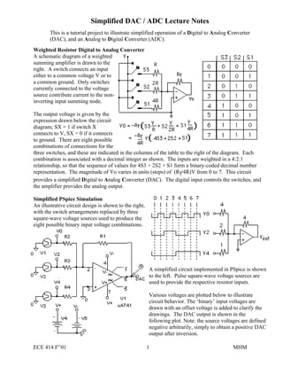
  • 1. ECE 414 F'’01 1 MHM Simplified DAC / ADC Lecture Notes This is a tutorial project to illustrate simplified operation of a Digital to Analog Converter (DAC), and an Analog to Digital Converter (ADC). Weighted Resistor Digital to Analog Converter A schematic diagram of a weighted summing amplifier is drawn to the right. A switch connects an input either to a common voltage V or to a common ground. Only switches currently connected to the voltage source contribute current to the non- inverting input summing node. The output voltage is given by the expression drawn below the circuit diagram; SX = 1 if switch X connects to V, SX = 0 if it connects to ground. There are eight possible combinations of connections for the three switches, and these are indicated in the columns of the table to the right of the diagram. Each combination is associated with a decimal integer as shown. The inputs are weighted in a 4:2:1 relationship, so that the sequence of values for 4S3 + 2S2 + S1 form a binary-coded decimal number representation. The magnitude of Vo varies in units (steps) of (Rf/4R)V from 0 to 7. This circuit provides a simplified Digital to Analog Converter (DAC). The digital input controls the switches, and the amplifier provides the analog output. Simplified PSpice Simulation An illustrative circuit design is shown to the right, with the switch arrangements replaced by three square-wave voltage sources used to produce the eight possible binary input voltage combinations. A simplified circuit implemented in PSpice is shown to the left. Pulse square-wave voltage sources are used to provide the respective resistor inputs. Various voltages are plotted below to illustrate circuit behavior. The ‘binary’ input voltages are drawn with an offset voltage is added to clarify the drawings. The DAC output is shown in the following plot. Note: the source voltages are defined negative arbitrarily, simply to obtain a positive DAC output after inversion.
  • 2. ECE 414 F'’01 2 MHM Alternative DAC Implementation An alternative DAC illustration (Schematics) is drawn below. V0, V1, and V4 are square-wave pulse sources with periods of 0.5ms, 1.0ms, and 2.0 ms respectively. The voltage-controlled switch pairs are operated so that when one switch is opened the other is closed, and vice-versa. A switch pair thus either connects Vref (=1v) to a weighted-resistor input, or the connection is to ground. (Incidentally open- and closed switch resistances are set to1 megohm and 1 ohm respectively.) The DAC output is plotted below, as well as the several summing input voltages.
  • 3. ECE 414 F'’01 3 MHM R-2R Ladder DAC The upper circuit in the figure to the right illustrates a section of a periodic network; the input resistance of the section is R. The second network cascades a second section onto the first, replacing the 2r termination resistor. Finally a third section is added to provide a three-bit binary current division. (Additional sections not used for this illustration can be added.) In the circuit below a three-section R-2R ladder is connected to a switch network so that either a fixed voltage V is applied to each section as shown, or a ground connection is made. The current contribution through each switch (apply superposition) is as noted; Sx is a binary variable which has the value 1 is the voltage connection is made, and the value 0 for a ground connection. The current from the ladder is fed to an inverting amplifier, and the output voltage Vo is
  • 4. ECE 414 F'’01 4 MHM PSpice Simulation Waveforms for a PSpice simulation of a 3-bit R-2R ladder DAC using square-wave pulse voltage sources in place of switches are drawn below; the Schematics diagram for the circuit follows. Current-Switched R-2R DAC In general switching a voltage is not favored because inevitable circuit capacitance tends to slow the switching; it is preferable to switch currents since circuit inductances are less troublesome. An illustrative current-switched R-2R DAC circuit diagram is drawn below. A JFET is used to provide switching operations in conjunction with fixed current sources driving the R- 2R ladder. When the JFET is cutoff the current source is connected into the ladder. For a zero gate- source voltage the JFET forms a low-resistance bypass around the current source
  • 5. ECE 414 F'’01 5 MHM DAC voltages are illustrated next.
  • 6. ECE 414 F'’01 6 MHM Simplified Analog to Digital Converter (ADC) There are several methods for ADC operation; ‘counting’, SAR comparison, dual ramp, flash, and tracking A ‘counting’ converter, whose simplicity is offset by relative slowness, simply compares the output of a DAC to the unknown analog input; when the DAC output first exceeds the analog input the conversion cycle is stopped and the DAC digital input at that time provides the ADC output. ‘Unknown’ input voltages of 2.5v and 6.5v respectively are input; see V(V8) below. The amplifier switches its output saturation state when the DAC voltage exceeds the ‘unknown’ voltage. Note that this means a finite voltage resolution.
  • 7. ECE 414 F'’01 7 MHM Successive Approximation Register (SAR) ADC The conversion time of the ‘counting’ converter must allow for the possibility that the maximum rated analog input voltage is applied, allow for a comparison at each step. The SAR ADC, while it operates in a similar manner, uses a much more efficient search process. Consider a three-bit conversion for simplicity. The counting ADC must allow for up to eight comparisons (including zero). The search tree for an SAR search is illustrated to the right. To start a conversion cycle a three-bit digital register is first cleared, and then loaded with the triplet 100. The register state provides the input to a DAC, and that provides a reference output. This output is compared to the analog signal to be converted, and a decision is made whether the analog signal is greater than or less than the reference signal. This comparison is essentially the same as that made for the ‘counting’ ADC, except that because of the use of the ‘half-way’ code the result of this single comparison is used to eliminate concurrently half the possible DAC steps. As the tree suggests, if the analog signal is greater then all the smaller DAC outputs are eliminated from consideration. Digital logic associated with the comparison then either clears the MSB (Most Significant Bit) to 0 or simply leaves it unchanged. In either case the next bit is set to 1, i.e., to the mid-code of the selected half, and a new comparison made. Again half the remaining DAC states are eliminated from consideration. Depending on the result of the comparison the second bit is cleared to 0, or it is left unchanged at 1. In either case the third bit is set to 1 and the comparison step repeated. Each time a comparison is made half the remaining DAC output states will be eliminated. Instead of having to step through 2N states for an N bit conversion only N comparisons are needed. The SAR ADC is perhaps the most common of the converters, providing a relatively rapid and relatively inexpensive conversion ‘Flash’ Converter Making all the comparisons between the digital states and the analog signal concurrently makes for a fast conversion cycle. A resistive voltage divider (see figure) can provide all the digital reference states required. There are eight reference values (including zero) for the three-bit converter illustrated. Note that the voltage reference states are offset so that they are midway between reference step values.. The analog signal is compared concurrently with each reference state; therefore a separate comparator is required for each comparison. Digital logic then combines the several comparator outputs to determine the appropriate binary code to present.
  • 8. ECE 414 F'’01 8 MHM A PSpice circuit configuration for a flash converter is illustrated below. (The evaluation version of PSpice sets various limits on the number of components that can be modeled. To simplify the circuit (while retaining the essential concepts) the comparator is replaced by a voltage-controlled switch (Sbreak) set to close when the unknown voltage (‘ana’ for analog) exceeds the reference voltage fr5om the resistive divider network by 0.1 volt, and open when the difference is less than zero. The ‘ON’ resistance of the switch is set to 1Ω, and the OFF resistance is 1 MegΩ. The ‘comparator’ output voltage is essentially zero when the switch is open and is 5v (chosen more or less arbitrarily as a representative logic voltage) when it is closed. The reference voltages are set to 0.5, 1.5, 2.5, 3.5, 4.5, 5.5, 6.5, and 7.5 volts respectively. The comparator outputs are labeled correspondingly as 1, 2, 3, 4, 5, 6, and 7 respectively. Note that if the unknown input voltage exceeds the voltage of level n then output n and all lower outputs are at 5 v. Digital logic to convert the ‘comparator’ outputs to appropriate bit values is drawn below the comparator circuit; inputs to the logic are the comparator outputs. The most significant bit B2 is 1 if output 4 is at 5 volts; this implies one of outputs 7, 6, 5, or 4 is at 5 volts. The next significant bit B! is 1 if either 7 or 6 is ‘high’, or if 4 is ‘low’ (MSB is 0) and concurrently 3 or 2 is ‘high’. The limited availability of parts in the evaluation version requires the use of a NOR gate and an inverter for the output. The least significant bit is 1 if 7 is high or if 5 is high but not 6 or 7). In addition the LSB is 1 if 4 is low, 3 is high, or if 4 and 2 both are low and 1 is high. Implementing this logic in spite of the limits of the evaluation version involved some modest contortions.
  • 9. ECE 414 F'’01 9 MHM The circuit as drawn is larger than the evaluation version of PSpice will allow. To bypass this constraint the digital computation is done in two parts. In the one case B2 and B1 are computed, and in the other B2 and B0 are computed. The two results are combined in a ‘paint’ program as drawn below. The analog input voltage V(ana) provided by the pulse source is set for pulse amplitudes of 2 (010) and 5 (101) volts respectively.
  • 10. ECE 414 F'’01 10 MHM