Efficient combinational logic circuit design using quantum dot cellular automata
•
2 j'aime•935 vues

Dr. Syed Hasan Saeed, Saifur Rehman, Mohd. Juned, Neelabh Tiwari, and Yogita Tiwari on ‘Efficient Combinational Logic Circuit Design Using Quantum Dot Cellular Automata’, in National Conferences on Challenges & Opportunities For Technological Innovation in India’ at ‘Ambalika Institute of Technology & Management, Lucknow, India’ on 16-02-2013.
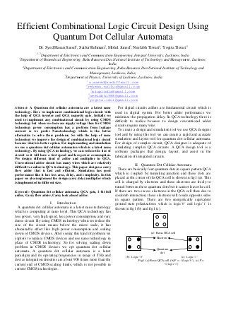
![By using this basic cell we can make QCA majority gate and IV. Circuit Design
QCA inverter, and QCA wire. A. 1-bit Full Adder
̅
Cout = (AB + BA) Cin + AB ̅
III. QCA Gate
̅
= ABCin + BACin + AB ̅
A. QCA Majority Gate
̅
= A (B + BCin) + ABCin ̅
The majority gate implements and simulates logic function.
̅
= A (B + B) (B + Cin) + ABCin ̅
If there are three input then output will be the majority of the
input. If there are A, B, C inputs then output will be = AB + ACin + ABCin ̅
Y = AB + BC + CA = AB + Cin (A + AB) ̅
= AB + Cin (A + A) (A + B) ̅
A = AB + CinA + BCin
= M (A, B, Cin)
̅
Cout = M (A, B, Cin) ̅ ̅ ̅ ……….. (1)
B Y ̅ ̅
Sum = (AB + BA) Cin + [(A + B) (B + A)] Cin ̅ ̅ ̅
̅ ̅ ̅ ̅
= ABCin + BACin + ABCin + BACin ̅ ̅
=A ̅ BCin + BACin + (AB + BA) Cin
̅ ̅ ̅ ̅ ̅
Device Cell ̅ ̅ ̅ ̅
= ABCin + BACin + [(AB + ACin + BCin) + ( BA + ACin ̅ ̅ ̅ ̅ ̅ ̅
̅ ̅
+ BCin)] Cin
C ̅
= ( AB + ACin + BCin) Cin + ( BA + ACin + BCin) Cin +̅ ̅ ̅ ̅ ̅ ̅ ̅
̅ ̅ ̅ ̅
(ACin + BCin) (ACin + BCin) ̅ ̅
Fig2. QCA Majority Gate ̅
= M (A, B, Cin) Cin + M (A, B, Cin) Cin + M (A, B, Cin) ̅ ̅ ̅ ̅
Figure (2) shows the QCA majority gate. If anyone input is ̅ ̅ ̅
M (A, B, Cin)
fixed i.e., it gives „0‟, it will work as an AND gate. If anyone = M (M (A, B, Cin), Cin, M (A, B, Cin)) ̅ ̅ ̅ ̅
input is fixed i.e., it gives „1‟, it will work as an OR gate. If A = M (M (A, B, Cin), Cin, Cout) ̅ ̅ ………. (2)
= „0‟, B = „1‟, and C = „1‟, so here „1‟ is in majority and in
that case output will be „1‟. If A = „1‟, B = „0‟, and C = „0‟, A
output will be „0‟ because „0‟ is in majority.
B
B. QCA Inverter
The most common inverter design is shown in fig (3). This Cin
inverter has two legs of the input QCA wire which interact at
45° angle with the first cell of the output wire. At this angle, M1 M2
the coupling between cells is negative and can be exploited to
realize the compliment function.
Cout
Y
A
M3
Sum
Fig (3) QCA Inverter
Following figure shows QCA inverter. Here A represents Fig (4) Schematic Diagram of 1-bit Full Adder
input and Y represents output.
Figure (4) shows the schematic diagram of 1-bit full adder.
Y=A
Here M1, M2, and M3 are the majority gate. A, B, Cin are
The above equation represents that if I give „0‟, we will get
three inputs.
„1‟ and if we give „1‟ then we will get „0‟.
Figure (5) shows the layout diagram of 1-bit full adder.](data:image/gif;base64,R0lGODlhAQABAIAAAAAAAP///yH5BAEAAAAALAAAAAABAAEAAAIBRAA7)
Recommandé
Recommandé
Contenu connexe
En vedette
En vedette (18)
Dernier
Dernier (20)
Efficient combinational logic circuit design using quantum dot cellular automata
- 1. Efficient Combinational Logic Circuit Design Using Quantum Dot Cellular Automata Dr. Syed Hasan Saeed1, Saifur Rehman2, Mohd. Juned3, Neelabh Tiwari4, Yogita Tiwari5 1, 2 Department of Electronics and Communication Engineering, Integral University, Lucknow, India 3 Department of Biomedical Engineering, Babu Banarasi Das National Institute of Technology and Management, Lucknow, India, 4 Department of Electronics and Communication Engineering, Babu Banarasi Das National Institute of Technology and Management, Lucknow, India, 5 Department of Physics, University of Lucknow, Lucknow, India 1 s.saeed@rediffmail.com 2 rehman.saifur@gmail.com 3 mjupindia@gmail.com 4 neelabh1988@gmail.com 5 yogita.idol@gmail.com Abstract- A Quantum dot cellular automata are a latest nano For digital circuits adders are fundamental circuit which is technology. Here we implement combinational logic circuit with used in digital system. For better adder performance we the help of QCA inverter and QCA majority gate. Initially we minimize the propagation delay. In QCA technology there is used to implement any combinational circuit by using CMOS difficult to realize because to design conventional adder technology but when we decrease supply voltage then for CMOS circuits require many wire. technology power consumption has a problem from leakage current so we prefer Nanotechnology which is the better To create a design and simulation tool we use QCA designer alternative to solve these problems. So with the help of nano tool and by using this tool we can create a rapid and accurate technology we improve the design of combinational logic circuit simulation and layout tool for quantum dot cellular automata. because which is better option. For implementing and simulation For design of complex circuit, QCA designer is adequate of we use a quantum dot cellular automaton which is a latest nano simulating complex QCA circuits. A QCA design tool is a technology. By using QCA technology, we can reduce the size of software packages that design, layout, and assist in the circuit so it will have a fast speed and less power consumption. fabrication of integrated circuits. We design different kind of adder and multiplier in QCA. Conventional adder circuit has many wires which are relatively II. Quantum Dot Cellular Automata difficult to realize in QCA technology. This paper designs a carry flow adder that is fast and efficient. Simulation has good There are basically four quantum dots in square pattern QCA performance like it has less area, delay, and complexity. In this which is coupled by tunneling junction and these dots are paper we also implement the design carry delay multiplier which placed at the corner of the QCA cell is shown in fig1 (a). This is implemented in different size. cell is charged by electrons and these electrons are freely to tunnel between these quantum dots but it cannot leave the cell. Keywords- Quantum dot cellular automata, QCA gate, 1-bit full If there are two excess electrons in the QCA cell then due to adder, Carry flow adder, Carry look ahead adder. coulomb interaction, these electrons will reside opposite sides in square pattern. There are two energetically equivalent I. Introduction ground state polarizations which is logic‟0‟ and logic‟1‟ is A quantum dot cellular automata is a latest nano technology shown in fig1 (b) and fig1 (c). which is computing at nano level. This QCA technology has less power, very high speed, less power consumption, and very dense circuit. By using CMOS technology when we reduce the size of the circuit means below the micro scale, it has abominable effect like high power consumption and scaling down of CMOS devices. After seeing this kind of problem we (a) Basic QCA cell explore to replace CMOS devices and use nano technology in Electron place of CMOS technology. So for solving scaling down problem in CMOS devices we opt quantum dot cellular Quantum automata. A quantum dot cellular automata is a latest dot paradigm and its operating frequencies in range of THz and (b) Logic „0‟ (c) Logic „1‟ device integration densities are about 900 times more than the Fig1. (a) Basic QCA cell, (b) P = -1(logic‟0‟), (c) P = current end of CMOS scaling limits, which is not possible in +1(logic‟1‟) current CMOS technologies.
- 2. By using this basic cell we can make QCA majority gate and IV. Circuit Design QCA inverter, and QCA wire. A. 1-bit Full Adder ̅ Cout = (AB + BA) Cin + AB ̅ III. QCA Gate ̅ = ABCin + BACin + AB ̅ A. QCA Majority Gate ̅ = A (B + BCin) + ABCin ̅ The majority gate implements and simulates logic function. ̅ = A (B + B) (B + Cin) + ABCin ̅ If there are three input then output will be the majority of the input. If there are A, B, C inputs then output will be = AB + ACin + ABCin ̅ Y = AB + BC + CA = AB + Cin (A + AB) ̅ = AB + Cin (A + A) (A + B) ̅ A = AB + CinA + BCin = M (A, B, Cin) ̅ Cout = M (A, B, Cin) ̅ ̅ ̅ ……….. (1) B Y ̅ ̅ Sum = (AB + BA) Cin + [(A + B) (B + A)] Cin ̅ ̅ ̅ ̅ ̅ ̅ ̅ = ABCin + BACin + ABCin + BACin ̅ ̅ =A ̅ BCin + BACin + (AB + BA) Cin ̅ ̅ ̅ ̅ ̅ Device Cell ̅ ̅ ̅ ̅ = ABCin + BACin + [(AB + ACin + BCin) + ( BA + ACin ̅ ̅ ̅ ̅ ̅ ̅ ̅ ̅ + BCin)] Cin C ̅ = ( AB + ACin + BCin) Cin + ( BA + ACin + BCin) Cin +̅ ̅ ̅ ̅ ̅ ̅ ̅ ̅ ̅ ̅ ̅ (ACin + BCin) (ACin + BCin) ̅ ̅ Fig2. QCA Majority Gate ̅ = M (A, B, Cin) Cin + M (A, B, Cin) Cin + M (A, B, Cin) ̅ ̅ ̅ ̅ Figure (2) shows the QCA majority gate. If anyone input is ̅ ̅ ̅ M (A, B, Cin) fixed i.e., it gives „0‟, it will work as an AND gate. If anyone = M (M (A, B, Cin), Cin, M (A, B, Cin)) ̅ ̅ ̅ ̅ input is fixed i.e., it gives „1‟, it will work as an OR gate. If A = M (M (A, B, Cin), Cin, Cout) ̅ ̅ ………. (2) = „0‟, B = „1‟, and C = „1‟, so here „1‟ is in majority and in that case output will be „1‟. If A = „1‟, B = „0‟, and C = „0‟, A output will be „0‟ because „0‟ is in majority. B B. QCA Inverter The most common inverter design is shown in fig (3). This Cin inverter has two legs of the input QCA wire which interact at 45° angle with the first cell of the output wire. At this angle, M1 M2 the coupling between cells is negative and can be exploited to realize the compliment function. Cout Y A M3 Sum Fig (3) QCA Inverter Following figure shows QCA inverter. Here A represents Fig (4) Schematic Diagram of 1-bit Full Adder input and Y represents output. Figure (4) shows the schematic diagram of 1-bit full adder. Y=A Here M1, M2, and M3 are the majority gate. A, B, Cin are The above equation represents that if I give „0‟, we will get three inputs. „1‟ and if we give „1‟ then we will get „0‟. Figure (5) shows the layout diagram of 1-bit full adder.
- 3. C. Carry Look Ahead Adder It is one kind of adder which is basically used in digital logic. A carry look ahead adder improves speed by reducing the amount of time required to determine carry bits. The Carry Look Ahead Adder is able to generate carries before the sum is produced using the propagate and generate logic to make addition much faster Cout = M (A, B, Cin) ̄ Sum = M (M (ā, b, cᵢ), M (a, b, cᵢ), M (a, b, cᵢ)) ̄ Fig (5) Layout Diagram of 1-bit Full Adder B. Carry Flow Adder To design a carry flow adder using 1-bit full adder to add N- bit numbers. Here we are designing 4-bit carry flow adder. In the carry flow adder carry output of the first full adder is the input of the second full adder. Figure (5) represents carry flow adder. A3 B3 A2 B2 A1 B1 A0 B0 Fig (8) Layout of Carry Look Ahead Adder Figure (8) shows the layout diagram of carry look ahead 1- 1- 1- 1- adder. bit bit bit bit Cout Cin full full full full V. Layout and Simulation Results add add add add er er er er S3 S2 S1 S0 Fig (6) Schematic Diagram of Carry Flow Adder In the following diagram A0, B0, A1, B1, A2, B2, A3, B3 are the input of carry flow adder and C0 is also the input of carry flow adder. Cout, S0, S1, S2, S3 is the output of carry flow adder. Fig (9) Simulation of 1-bit Full Adder Figure (9) shows the simulation result of 1-bit full adder. The input and output waveform of 1-bit full adder is shown in figure (9). VI. Conclusion Quantum cellular automata have basically wire delay. For fast switching speed we reduce the complexity of the circuit. Fig (7) Layout Diagram of Carry Flow Adder In this project we are implementing the carry flow adder and carry look ahead adder by using quantum dot cellular Figure (7) shows the layout diagram of carry flow adder. automata. By taking the help of nanotechnology we can reduce
- 4. the size of the circuit and can reduce power also. By giving the logical interpretation we can increase the speed of adder circuit and can reduce the area of adder circuit also. References [1]. Heumpil Cho, and Earl E. Swartzlander, Jr., “Adder and Multiplier Design in Quantum-Dot Cellular Automata”, IEEE Trans. On Computers, vol. 58, no. 6, June 2009. [2]. H. Cho and E.E. Swartzlander, Jr., “Serial Parallel Multiplier Design in Quantum-Dot Cellular Automata,” Proc. 18th IEEE Symp. Computer Arithmetic, pp. 7-15, 2007. [3]. K. Walus, T. Dysart, G. Jullien, and R. Budiman, “QCA Designer: A Rapid Design and Simulation Tool for Quantum-Dot Cellular Automata,” IEEE Trans. Nanotechnology, vol. 3, no. 1, pp. 26-29, Mar. 2004. [4]. H. Cho and E.E. Swartzlander, Jr., “Adder Designs and Analyses for Quantum-Dot Cellular Automata,” IEEE Trans. Nanotechnology, vol. 6, no. 3, pp. 374-383, May 2007. [5]. R. Zhang, K. Walus, W. Wang, and G.A. Jullien, “Performance Comparison of Quantum-Dot Cellular Automata Adders,” Proc. IEEE Int’l Symp. Circuits and Systems, vol. 3, pp. 2522-2526, 2005. [6]. W. Wang, K. Walus, and G.A. Jullien, “Quantum-Dot Cellular Automata Adders,” Proc. Third IEEE Conf. Nanotechnology, pp. 461-464, 2003. [7]. Zhang R. et al. “A Method of Majority Logic Reduction for Quantum Cellular Automata”, IEEE Transaction on Nanotechnology, December 2004, 3(4) 443-450p. [8]. R. Meo, “Majority Gate Networks”, IEEE Transaction, Electronic Computers. 15, (606-618)(1966). [9]. A. Vetteth et al., “Quantum-Dot Cellular Automata Carry-Look- Ahead Adder and Barrel Shifter”, Proc. IEEE Emerging Telecomm. Technologies Conf., Sept. 2002. [10]. C.S. Lent, P.D. Tougaw, W. Porod, and G.H. Bernstein, “Quantum Cellular Automata”, Nanotechnology, vol. 4, no. 1 pp. 49-57, Jan. 1993. [11]. R. Zhang, F. Zhang, and Y. B. Kim, “Quantum-Dot Cellular Automata Spice Macro Model”, Proc. ACM Great Lakes Symp. VLSI, pp. 108-111, 2005.